![]() HDMI Arria 10 FPGA IP Design Example
HDMI Arria 10 FPGA IP Design Example
User Guide HDMI Intel® Arria 10 FPGA IP
Design Example User Guide
Updated for Intel®Quartus®
Prime Design Suite: 22.4
IP Version: 19.7.1
HDMI Intel® FPGA IP Design Example Quick Start Guide for Intel® Arria® 10 Devices
The HDMI Intel® 10 devices features a simulating testbench and a hardware design that supports compilation and hardware testing.
FPGA IP design example for Intel Arria®
The HDMI Intel FPGA IP offers the following design examples:
- HDMI 2.1 RX-TX retransmit design with fixed rate link (FRL) mode enabled
- HDMI 2.0 RX-TX retransmit design with FRL mode disabled
- HDCP over HDMI 2.0 design
Note: The HDCP feature is not included in the Intel® Quartus Prime Pro Edition software.
To access the HDCP feature, contact Intel at https://www.intel.com/content/www/us/en/broadcast/products/programmable/applications/connectivity-solutions.html.
When you generate a design example, the parameter editor automatically creates the files necessary to simulate, compile, and test the design in hardware.
Figure 1. Development Steps Related Information
HDMI Intel FPGA IP User Guide
1.1. Generating the Design
Use the HDMI Intel FPGA IP parameter editor in the Intel Quartus Prime software to generate the design examples. Intel Corporation. All rights reserved. Intel, the Intel logo, and other Intel marks are trademarks of Intel Corporation or its subsidiaries. Intel warrants performance of its FPGA and semiconductor products to current specifications in accordance with Intel’s standard warranty, but reserves the right to make changes to any products and services at any time without notice. Intel assumes no responsibility or liability arising out of the application or use of any information, product, or service described herein except as expressly agreed to in writing by Intel. Intel customers are advised to obtain the latest version of device specifications before relying on any published information and before placing orders for products or services. *Other names and brands may be claimed as the property of others.
Starting with the Nios® II EDS in the Intel Quartus Prime Pro Edition software version 19.2 and Intel Quartus Prime Standard Edition software version 19.1, Intel has removed the Cygwin component in the Windows* version of Nios II EDS, replacing it with Windows* Subsytem for Linux (WSL). If you are a Windows* user, you need to install WSL prior to generating your design example.
Figure 2. Generating the Design Flow
- Create a project targeting Intel Arria 10 device family and select the desired device.
- In the IP Catalog, locate and double-click Interface Protocols ➤ Audio & Video ➤ HDMI Intel FPGA IP. The New IP Variant or New IP Variation window appears.
- Specify a top-level name for your custom IP variation. The parameter editor saves the IP variation settings in a file named <your_ip>.ip or <your_ip>.qsys.
- Click OK. The parameter editor appears.
- On the IP tab, configure the desired parameters for both TX and RX.
- Turn on the Support FRL parameter to generate the HDMI 2.1 design example in FRL mode. Turn it off to generate the HDMI 2.0 design example without FRL.
- On the Design Example tab, select Arria 10 HDMI RX-TX Retransmit.
- Select Simulation to generate the testbench, and select Synthesis to generate the hardware design example.You must select at least one of these options to generate the design example files. If you select both, the generation time is longer.
- For Generate File Format, select Verilog or VHDL.
- For Target Development Kit, select Intel Arria 10 GX FPGA Development Kit. If you select a development kit, then the target device (selected in step 4) changes to match the device on target board. For Intel Arria 10 GX FPGA Development Kit, the default device is 10AX115S2F4I1SG.
- Click Generate Example Design.
Related Information
How to install the Windows* Subsystem for Linux* (WSL) on Windows* OS?
1.2. Simulating the Design
The HDMI testbench simulates a serial loopback design from a TX instance to an RX instance. Internal video pattern generator, audio sample generator, sideband data generator, and auxiliary data generator modules drive the HDMI TX instance and the serial output from the TX instance connects to the RX instance in the testbench.
Figure 3. Design Simulation Flow
- Go to the desired simulation folder.
- Run the simulation script for the supported simulator of your choice. The script compiles and runs the testbench in the simulator.
- Analyze the results.
Table 1. Steps to Run Simulation
| Simulator | Working Directory | Instructions |
| Riviera-PRO* | /simulation/aldec | In the command line, type |
| vsim -c -do aldec.do | ||
| ModelSim* | /simulation/mentor | In the command line, type |
| vsim -c -do mentor.do | ||
| VCS* | /simulation/synopsys/vcs | In the command line, type |
| source vcs_sim.sh | ||
| VCS MX | /simulation/synopsys/ vcsmx | In the command line, type |
| source vcsmx_sim.sh | ||
| Xcelium* Parallel | /simulation/xcelium | In the command line, type |
| source xcelium_sim.sh |
A successful simulation ends with the following message:
# SYMBOLS_PER_CLOCK = 2
# VIC = 4
# FRL_RATE = 0
# BPP = 0
# AUDIO_FREQUENCY (kHz) = 48
# AUDIO_CHANNEL = 8
# Simulation pass
1.3. Compiling and Testing the Design
To compile and run a demonstration test on the hardware example design, follow these steps:
- Ensure hardware example design generation is complete.
- Launch the Intel Quartus Prime software and open the .qpf file.
• HDMI 2.1 design example with Support FRL enabled: project directory/quartus/a10_hdmi21_frl_demo.qpf
• HDMI 2.0 design example with Support FRL disabled: projectd irectory/quartus/a10_hdmi2_demo.qpf - Click Processing ➤ Start Compilation.
- After successful compilation, a .sof file will be generated in the quartus/output_files directory.
- Connect to the on-board FMC port B (J2):
• HDMI 2.1 design example with Support FRL enabled: Bitec HDMI 2.1 FMC Daughter Card Rev 9
Note: You can select the revision of your Bitec HDMI daughter card. Under the Design Example tab, set HDMI Daughter Card Revision to either Revision 9, Revision or no daughter card. The default value is Revision 9.
• HDMI 2.0 design example with Support FRL disabled: Bitec HDMI 2.0 FMC Daughter Card Rev 11 - Connect TX (P1) of the Bitec FMC daughter card to an external video source.
- Connect RX (P2) of the Bitec FMC daughter card to an external video sink or video analyzer.
- Ensure all switches on the development board are in default position.
- Configure the selected Intel Arria 10 device on the development board using the generated .sof file (Tools ➤ Programmer ).
- The analyzer should display the video generated from the source.
Related Information
Intel Arria 10 FPGA Development Kit User Guide
1.4. HDMI Intel FPGA IP Design Example Parameters
Table 2.
HDMI Intel FPGA IP Design Example Parameters for Intel Arria 10 Devices These options are available for Intel Arria 10 devices only.
| Parameter | Value |
Description |
| Available Design Example | ||
| Select Design | Arria 10 HDMI RX-TX Retransmit | Select the design example to be generated. |
|
Design Example Files |
||
| Simulation | On, Off | Turn on this option to generate the necessary files for the simulation testbench. |
| Synthesis | On, Off | Turn on this option to generate the necessary files for Intel Quartus Prime compilation and hardware demonstration. |
|
Generated HDL Format |
||
| Generate File Format | Verilog, VHDL | Select your preferred HDL format for the generated design example fileset. Note: This option only determines the format for the generated top level IP files. All other files (e.g. example testbenches and top level files for hardware demonstration) are in Verilog HDL format |
|
Target Development Kit |
||
| Select Board | No Development Kit, | Select the board for the targeted design example. |
| Arria 10 GX FPGA Development Kit,
Custom Development Kit |
• No Development Kit: This option excludes all hardware aspects for the design example. The IP core sets all pin assignments to virtual pins. • Arria 10 GX FPGA Development Kit: This option automatically selects the project’s target device to match the device on this development kit. You may change the target device using the Change Target Device parameter if your board revision has a different device variant. The IP core sets all pin assignments according to the development kit. |
|
| •Custom Development Kit: This option allows the design example to be tested on a third party development kit with an Intel FPGA. You may need to set the pin assignments on your own. | ||
|
Target Device |
||
| Change Target Device | On, Off | Turn on this option and select the preferred device variant for the development kit. |
HDMI 2.1 Design Example (Support FRL = 1)
The HDMI 2.1 design example in FRL mode demonstrates one HDMI instance parallel loopback comprising four RX channels and four TX channels.
Table 3. HDMI 2.1 Design Example for Intel Arria 10 Devices
| Design Example | Data Rate | Channel Mode |
Loopback Type |
| Arria 10 HDMI RX-TX Retransmit | • 12 Gbps (FRL) • 10 Gbps (FRL) • 8Gbps (FRL) • 6 Gbps (FRL) • 3 Gbps (FRL) • <6 Gbps (TMDS) |
Simplex | Parallel with FIFO buffer |
Features
- The design instantiates FIFO buffers to perform a direct HDMI video stream passthrough between the HDMI 2.1 sink and source.
- The design is capable to switch between FRL mode and TMDS mode during run time.
- The design uses LED status for early debugging stage.
- The design comes with HDMI RX and TX instances.
- The design demonstrates the insertion and filtering of Dynamic Range and Mastering (HDR) InfoFrame in RX-TX link module.
- The design negotiates the FRL rate between the sink connected to TX and the source connected to RX. The design passes through the EDID from the external sink to the on-board RX in default configuration. The Nios II processor negotiates the link base on the capability of the sink connected to TX. You can also toggle the user_dipsw on-board switch to manually control the TX and RX FRL capabilities.
- The design includes several debugging features.
The RX instance receives a video source from the external video generator, and the data then goes through a loopback FIFO before it is transmitted to the TX instance. You need to connect an external video analyzer, monitor, or a television with HDMI connection to the TX core to verify the functionality.
2.1. HDMI 2.1 RX-TX Retransmit Design Block Diagram
The HDMI RX-TX retransmit design example demonstrates parallel loopback on simplex channel mode for HDMI 2.1 with Support FRL enabled.
Figure 4. HDMI 2.1 RX-TX Retransmit Block Diagram 2.2. Creating RX-Only or TX-Only Designs
For advanced users, you can use the HDMI 2.1 design to create a TX- or RX-only design.
Figure 5. Components Required for RX-Only or TX-Only Design To use RX- or TX-only components, remove the irrelevant blocks from the design.
Table 4. RX-Only and TX-Only Design Requirements
| User Requirements | Preserve | Remove |
Add |
| HDMI RX only | RX Top | • TX Top • RX-TX Link • CPU Subsystem • Transceiver Arbiter |
– |
| HDMI TX only | •TX Top •CPU Sub-System |
•RX Top • RX-TX Link •Transceiver Arbiter |
Video Pattern Generator(custom module or generated from the Video and Image Processing (VIP) Suite) |
Besides the RTL changes, you need to also edit the main.c script.
• For HDMI TX-only designs, decouple the wait for the HDMI RX lock status by removing the following lines and replace with
tx_xcvr_reconfig(tx_frl_rate);
rx_hdmi_lock = READ_PIO(PIO_IN0_BASE, PIO_RX_LOCKED_OFFSET,
PIO_RX_LOCKED_WIDTH);
while (rx_hdmi_lock == 0) {
if (check_hpd_isr()) { break; }
// rx_vid_lock = READ_PIO(PIO_IN0_BASE, PIO_VID_LOCKED_OFFSET,
PIO_VID_LOCKED_WIDTH);
rx_hdmi_lock = READ_PIO(PIO_IN0_BASE, PIO_RX_LOCKED_OFFSET,
PIO_RX_LOCKED_WIDTH);
// Reconfig Tx after rx is locked
if (rx_hdmi_lock == 1) {
if (READ_PIO(PIO_IN0_BASE, PIO_LOOPBACK_MODE_OFFSET,
PIO_LOOPBACK_MODE_WIDTH) == 1) {
rx_frl_rate = READ_PIO(PIO_IN0_BASE, PIO_RX_FRL_RATE_OFFSET,
PIO_RX_FRL_RATE_WIDTH);
tx_xcvr_reconfig(rx_frl_rate);
} else {
tx_xcvr_reconfig(tx_frl_rate);
} } }
• For HDMI RX-only designs, keep only the following lines in the main.c script:
REDRIVER_INIT();
hdmi_rx_init();
2.3. Hardware and Software Requirements
Intel uses the following hardware and software to test the design example.
Hardware
- Intel Arria 10 GX FPGA Development Kit
- HDMI 2.1 Source (Quantum Data 980 48G Generator)
- HDMI 2.1 Sink (Quantum Data 980 48G Analyzer)
- Bitec HDMI FMC 2.1 daughter card (Revision 9)
- HDMI 2.1 Category 3 cables (tested with Belkin 48Gbps HDMI 2.1 Cable)
Software
- Intel Quartus Prime Pro Edition software version 20.1
2.4. Directory Structure
The directories contain the generated files for the HDMI Intel FPGA IP design example.
Figure 6. Directory Structure for the Design Example Table 5. Generated RTL Files
| Folders | Files/Subfolders |
| common | clock_control.ip |
| clock_crosser.v | |
| dcfifo_inst.v | |
| edge_detector.sv | |
| fifo.ip | |
| output_buf_i2c.ip |
| test_pattern_gen.v | |
| tpg.v | |
| tpg_data.v | |
| gxb | gxb_rx.ip |
| gxb_rx_reset.ip | |
| gxb_tx.ip | |
| gxb_tx_fpll.ip | |
| gxb_tx_reset.ip | |
| hdmi_rx | hdmi_rx.ip |
| hdmi_rx_top.v | |
| Panasonic.hex | |
| hdmi_tx | hdmi_tx.ip |
| hdmi_tx_top.v | |
| i2c_slave | i2c_avl_mst_intf_gen.v |
| i2c_clk_cnt.v | |
| i2c_condt_det.v | |
| i2c_databuffer.v | |
| i2c_rxshifter.v | |
| i2c_slvfsm.v | |
| i2c_spksupp.v | |
| i2c_txout.v | |
| i2c_txshifter.v | |
| i2cslave_to_avlmm_bridge.v | |
| pll | pll_hdmi_reconfig.ip |
| pll_frl.ip | |
| pll_reconfig_ctrl.v | |
| pll_tmds.ip | |
| pll_vidclk.ip | |
| quartus.ini | |
| rxtx_link | altera_hdmi_hdr_infoframe.v |
| aux_mux.qsys | |
| aux_retransmit.v | |
| aux_src_gen.v | |
| ext_aux_filter.v |
| rxtx_link.v | |
| scfifo_vid.ip | |
| reconfig | mr_rx_iopll_tmds/ |
| mr_rxphy/ | |
| mr_tx_fpll/ | |
| altera_xcvr_functions.sv | |
| mr_compare.sv | |
| mr_rate_detect.v | |
| mr_rx_rate_detect_top.v | |
| mr_rx_rcfg_ctrl.v | |
| mr_rx_reconfig.v | |
| mr_tx_rate_detect_top.v | |
| mr_tx_rcfg_ctrl.v | |
| mr_tx_reconfig.v | |
| rcfg_array_streamer_iopll.sv | |
| rcfg_array_streamer_rxphy.sv | |
| rcfg_array_streamer_rxphy_xn.sv | |
| rcfg_array_streamer_txphy.sv | |
| rcfg_array_streamer_txphy_xn.sv | |
| rcfg_array_streamer_txpll.sv | |
| sdc | a10_hdmi2.sdc |
| jtag.sdc |
Table 6. Generated Simulation Files
Refer to the Simulation Testbench section for more information
| Folders | Files |
| aldec | /aldec.do |
| /rivierapro_setup.tcl | |
| cadence | /cds.lib |
| /hdl.var | |
| <cds_libs folder> | |
| mentor | /mentor.do |
| /msim_setup.tcl | |
| synopsys | /vcs/filelist.f |
| /vcs/vcs_setup.sh |
| /vcs/vcs_sim.sh | |
| /vcsmx/synopsys_sim_setup | |
| /vcsmx/vcsmx_setup.sh | |
| /vcsmx/vcsmx_sim.sh | |
| xcelium | /cds.lib |
| /hdl.var | |
| /xcelium_setup.sh | |
| /xcelium_sim.sh | |
| <cds_libs folder> | |
| common | /modelsim_files.tcl |
| /riviera_files.tcl | |
| /vcs_files.tcl | |
| /vcsmx_files.tcl | |
| /xcelium_files.tcl | |
| hdmi_rx | /hdmi_rx.ip |
| /Panasonic.hex | |
| hdmi_tx | /hdmi_tx.ip |
Table 7. Generated Software Files
| Folders | Files |
| tx_control_src Note: The tx_control folder also contains duplicates of these files. |
global.h |
| hdmi_rx.c | |
| hdmi_rx.h | |
| hdmi_tx.c | |
| hdmi_tx.h | |
| hdmi_tx_read_edid.c | |
| hdmi_tx_read_edid.h | |
| intel_fpga_i2c.c | |
| intel_fpga_i2c.h | |
| main.c | |
| pio_read_write.c | |
| pio_read_write.h |
2.5. Design Components
The HDMI Intel FPGA IP design example consists of the common top-level components and HDMI TX and RX top components.
2.5.1. HDMI TX Components
The HDMI TX top components include the TX core top-level components, and the IOPLL, transceiver PHY reset controller, transceiver native PHY, TX PLL, TX reconfiguration management, and the output buffer blocks.
Figure 7. HDMI TX Top Components Table 8. HDMI TX Top Components
|
Module |
Description |
| HDMI TX Core | The IP receives video data from the top level and performs auxiliary data encoding, audio data encoding, video data encoding, scrambling, TMDS encoding or packetization. |
| IOPLL | The IOPLL (iopll_frl) generates the FRL clock for the TX core. This reference clock receives the TX FPLL output clock. FRL clock frequency = Data rate per lanes x 4 / (FRL characters per clock x 18) |
| Transceiver PHY Reset Controller | The Transceiver PHY reset controller ensures a reliable initialization of the TX transceivers. The reset input of this controller is triggered from the top level, and it generates the corresponding analog and digital reset signal to the Transceiver Native PHY block according to the reset sequencing inside the block. The tx_ready output signal from this block also functions as a reset signal to the HDMI Intel FPGA IP to indicate the transceiver is up and running, and ready to receive data from the core. |
| Transceiver Native PHY | Hard transceiver block that receives the parallel data from the HDMI TX core and serializes the data from transmitting it. Note: To meet the HDMI TX inter-channel skew requirement, set the TX channel bonding mode option in the Intel Arria 10 Transceiver Native PHY parameter editor to PMA and PCS bonding. You also need to add the maximum skew (set_max_skew) constraint requirement to the digital reset signal from the transceiver reset controller (tx_digitalreset) as recommended in the Intel Arria 10 Transceiver PHY User Guide. |
| TX PLL | The transmitter PLL block provides the serial fast clock to the Transceiver Native PHY block. For this HDMI Intel FPGA IP design example, fPLL is used as TX PLL. TX PLL has two reference clocks. • Reference clock 0 is connected to the programmable oscillator (with TMDS clock frequency) for TMDS mode. In this design example, RX TMDS clock is used to connect to reference clock 0 for TMDS mode. Intel recommends you to use programmable oscillator with TMDS clock frequency for reference clock 0. • Reference clock 1 is connected to a fixed 100 MHz clock for FRL mode. |
| TX Reconfiguration Management | •In TMDS mode, the TX reconfiguration management block reconfigures the TX PLL for different output clock frequency according to the TMDS clock frequency of the specific video. •In FRL mode, the TX reconfiguration management block reconfigures the TX PLL to supply the serial fast clock for 3 Gbps, 6 Gbps, 8 Gbps, 10 Gbps and 12 Gbps according to FRL_Rate field in the 0x31 SCDC register. •The TX reconfiguration management block switches the TX PLL reference clock between reference clock 0 for TMDS mode and reference clock 1 for FRL mode. |
| Output buffer | This buffer acts as an interface to interact the I2C interface of the HDMI DDC and redriver components. |
Table 9.Transceiver Data Rate and Oversampling Factor Each Clock Frequency Range
| Mode | Data Rate | Oversampler 1 (2x oversample) | Oversampler 2 (4x oversample) | Oversample Factor | Oversampled Data Rate (Mbps) |
| TMDS | 250–1000 | On | On | 8 | 2000–8000 |
| TMDS | 1000–6000 | On | Off | 2 | 2000–12000 |
| FRL | 3000 | Off | Off | 1 | 3000 |
| FRL | 6000 | Off | Off | 1 | 6000 |
| FRL | 8000 | Off | Off | 1 | 8000 |
| FRL | 10000 | Off | Off | 1 | 10000 |
| FRL | 12000 | Off | Off | 1 | 12000 |
Figure 8. TX Reconfiguration Sequence Flow 2.5.2. HDMI RX Components
The HDMI RX top components include the RX core top-level components, optional I²C slave and EDID RAM, IOPLL, transceiver PHY reset controller, RX native PHY, and the RX reconfiguration management blocks.
Figure 9. HDMI RX Top Components Table 10. HDMI RX Top Components
|
Module |
Description |
| HDMI RX Core | The IP receives the serial data from the Transceiver Native PHY and performs data alignment, channel deskew, TMDS decoding, auxiliary data decoding, video data decoding, audio data decoding, and descrambling. |
| I2C Slave | I2C is the interface used for Sink Display Data Channel (DDC) and Status and Data Channel (SCDC). The HDMI source uses the DDC to determine the capabilities and characteristics of the sink by reading the Enhanced Extended Display Identification Data (E-EDID) data structure. The 8-bit I2C slave addresses for E-EDID are 0xA0 and 0xA1. The LSB indicates the access type: 1 for read and 0 for write. When an HPD event occurs, the I2C slave responds to E-EDID data by reading from the on-chip The I2C slave-only controller also supports SCDC for HDMI 2.0 and 2.1 The 9-bit I2C slave address for the SCDC are 0xA8 and 0xA9. When an HPD event occurs, the I2C slave performs write or read transaction to or from SCDC interface of the HDMI RX core. Link training process for Fixed Rate Link (FRL) also happens through I2C During an HPD event or when the source writes a different FRL rate to the FRL Rate register (SCDC registers 0x31 bit[3:0]), the link training process starts. Note: This I2C slave-only controller for SCDC is not required if HDMI 2.0 or HDMI 2.1 is not intended |
| EDID RAM | The design stores the EDID information using the RAM 1-Port IP. A standard two- wire (clock and data) serial bus protocol (I2C slave-only controller) transfers the CEA-861-D Compliant E-EDID data structure. This EDID RAM stores the E-EDID information. •When in TMDS mode, the design supports EDID passthrough from TX to RX. During EDID passthrough, when the TX is connected to the external sink, the Nios II processor reads the EDID from the external sink and writes to the EDID RAM. • When in FRL mode, the Nios II processor writes the pre-configured EDID for each link rate based on the HDMI_RX_MAX_FRL_RATE parameter in the global.h script. Use the following HDMI_RX_MAX_FRL_RATE inputs for the supported FRL rate: • 1: 3G 3 Lanes • 2: 6G 3 Lanes •3: 6G 4 Lanes • 4: 8G 4 Lanes •5: 10G 4 Lanes (default) •6: 12G 4 Lanes |
| IOPLL | The HDMI RX uses two IOPLLs. • The first IOPLL (pll_tmds) generates the RX CDR reference clock. This IOPLL is only used in TMDS mode. The reference clock of this IOPLL receives the TMDS clock. The TMDS mode uses this IOPLL because the CDR cannot receive reference clocks below 50 MHz and the TMDS clock frequency ranges from 25 MHz to 340 MHz. This IOPLL provides clock frequency that is 5 times of the input reference clock for frequency range between 25 MHz to 50 MHz and provides the same clock frequency as input reference clock for frequency range between 50 MHz to 340 MHz. •The second IOPLL (iopll_frl) generates the FRL clock for the RX core. This reference clock receives the CDR recovered clock. FRL clock frequency = Data rate per lanes x 4 / (FRL characters per clock x 18) |
| Transceiver PHY Reset Controller | The Transceiver PHY reset controller ensures a reliable initialization of the RX transceivers. The reset input of this controller is triggered by the RX reconfiguration, and it generates the corresponding analog and digital reset signal to the Transceiver Native PHY block according to the reset sequencing inside the block. |
| RX Native PHY | Hard transceiver block that receives the serial data from an external video source. It deserializes the serial data to parallel data before passing the data to the HDMI RX core. This block runs on Enhanced PCS for FRL mode. RX CDR has two reference clocks. • Reference clock 0 is connected to output clock of IOPLL TMDS (pll_tmds), which is derived from the TMDS clock. • Reference clock 1 is connected to a fixed 100 MHz clock. In TMDS mode, RX CDR is reconfigured to select reference clock 0, and in FRL mode, RX CDR is reconfigured to select reference clock 1. |
| RX Reconfiguration Management | In TMDS mode, the RX reconfiguration management block implements rate detection circuitry with the HDMI PLL to drive the RX transceiver to operate at any arbitrary link rates ranging from 250 Mbps to 6,000 Mbps. In FRL mode, the RX reconfiguration management block reconfigures the RX transceiver to operate at 3 Gbps, 6 Gbps, 8 Gbps, 10 Gbps, or 12 Gbps depending on the FRL rate in the SCDC_FRL_RATE register field (0x31[3:0]). The RX reconfiguration management block switches between Standard PCS/RX for TMDS mode and Enhanced PCS for FRL mode.Refer to Figure 10 on page 22. |
Figure 10. RX Reconfiguration Sequence Flow
The figure illustrates the multi-rate reconfiguration sequence flow of the controller when it receives input data stream and reference clock frequency, or when the transceiver is unlocked. 2.5.3. Top-Level Common Blocks
The top-level common blocks include the transceiver arbiter, the RX-TX link components, and the CPU subsystem.
Table 11. Top-Level Common Blocks
|
Module |
Description |
| Transceiver Arbiter | This generic functional block prevents transceivers from recalibrating simultaneously when either RX or TX transceivers within the same physical channel require reconfiguration. The simultaneous recalibration impacts applications where RX and TX transceivers within the same channel are assigned to independent IP implementations. This transceiver arbiter is an extension to the resolution recommended for merging simplex TX and simplex RX into the same physical channel. This transceiver arbiter also assists in merging and arbitrating the Avalon® memory- mapped RX and TX reconfiguration requests targeting simplex RX and TX transceivers within a channel as the reconfiguration interface port of the transceivers can only be accessed sequentially. The interface connection between the transceiver arbiter and TX/RX Native PHY/PHY Reset Controller blocks in this design example demonstrates a generic mode that applies for any IP combination using the transceiver arbiter. The transceiver arbiter is not required when only either RX or TX transceiver is used in a channel. The transceiver arbiter identifies the requester of a reconfiguration through its Avalon memory-mapped reconfiguration interfaces and ensures that the corresponding tx_reconfig_cal_busy or rx_reconfig_cal_busy is gated accordingly. For HDMI applications, only RX initiates reconfiguration. By channeling the Avalon memory-mapped reconfiguration request through the arbiter, the arbiter identifies that the reconfiguration request originates from the RX, which then gates tx_reconfig_cal_busy from asserting and allows rx_reconfig_cal_busy to assert. The gating prevents the TX transceiver from being moved to calibration mode unintentionally. Note: Because HDMI only requires RX reconfiguration, the tx_reconfig_mgmt_* signals are tied off. Also, the Avalon memory- mapped interface is not required between the arbiter and the TX Native PHY block. The blocks are assigned to the interface in the design example to demonstrate generic transceiver arbiter connection to TX/RX Native PHY/PHY Reset Controller |
| RX-TX Link | • The video data output and synchronization signals from HDMI RX core loop through a DCFIFO across the RX and TX video clock domains. • The auxiliary data port of the HDMI TX core controls the auxiliary data that flow through the DCFIFO through backpressure. The backpressure ensures there is no incomplete auxiliary packet on the auxiliary data port. • This block also performs external filtering: — Filters the audio data and audio clock regeneration packet from the auxiliary data stream before transmitting to the HDMI TX core auxiliary data port. — Filters the High Dynamic Range (HDR) InfoFrame from the HDMI RX auxiliary data and inserts an example HDR InfoFrame to the auxiliary data of the HDMI TX through the Avalon streaming multiplexer. |
| CPU Subsystem | The CPU subsystem functions as SCDC and DDC controllers, and source reconfiguration controller. • The source SCDC controller contains the I2C master controller. The I2C master controller transfers the SCDC data structure from the FPGA source to the external sink for HDMI 2.0 operation. For example, if the outgoing data stream is 6,000 Mbps, the Nios II processor commands the I2C master controller to update the TMDS_BIT_CLOCK_RATIO and SCRAMBLER_ENABLE bits of the sink TMDS configuration register to 1. • The same I2C master also transfers the DDC data structure (E-EDID) between the HDMI source and external sink. • The Nios II CPU acts as the reconfiguration controller for the HDMI source. The CPU relies on the periodic rate detection from the RX Reconfiguration Management module to determine if the TX requires reconfiguration. The Avalon memory-mapped slave translator provides the interface between the Nios II processor Avalon memory-mapped master interface and the Avalon memory-mapped slave interfaces of the externally instantiated HDMI source’s IOPLL and TX Native PHY. • Perform link training through I2C master interface with external sink |
2.6. Dynamic Range and Mastering (HDR) InfoFrame Insertion and Filtering
The HDMI Intel FPGA IP design example includes a demonstration of HDR InfoFrame insertion in a RX-TX loopback system.
HDMI Specification version 2.0b allows Dynamic Range and Mastering InfoFrame to be transmitted through HDMI auxiliary stream. In the demonstration, the Auxiliary Packet Generator block supports the HDR insertion. You need only to format the intended HDR InfoFrame packet as specified in the module’s signal list table and the insertion of the HDR InfoFrame occurs once every video frame.
In this example configuration, in instances where the incoming auxiliary stream already includes HDR InfoFrame, the streamed HDR content is filtered. The filtering avoids conflicting HDR InfoFrames to be transmitted and ensures that only the values specified in the HDR Sample Data module are used.
Figure 11. RX-TX Link with Dynamic Range and Mastering InfoFrame Insertion
The figure shows the block diagram of RX-TX link including Dynamic Range and Mastering InfoFrame insertion into the HDMI TX core auxiliary stream. Table 12. Auxiliary Data Insertion Block (aux_retransmit) Signals
| Signal | Direction | Width |
Description |
| Clock and Reset | |||
| clk | Input | 1 | Clock input. This clock should be connected to the video clock. |
| reset | Input | 1 | Reset input. |
|
Auxiliary Packet Signals |
|||
| tx_aux_data | Output | 72 | TX Auxiliary packet output from the multiplexer. |
| tx_aux_valid | Output | 1 | |
| tx_aux_ready | Output | 1 | |
| tx_aux_sop | Output | 1 | |
| tx_aux_eop | Output | 1 | |
| rx_aux_data | Input | 72 | RX Auxiliary data passed to the packet filter module before entering the multiplexer. |
| rx_aux_valid | Input | 1 | |
| rx_aux_sop | Input | 1 | |
| rx_aux_eop | Input | 1 | |
| Control Signal | |||
| hdmi_tx_vsync | Input | 1 | HDMI TX Video Vsync. This signal should be synchronized to the link speed clock domain.The core inserts the HDR InfoFrame to the auxiliary stream at the rising edge of this signal |
Table 13. HDR Data Module (altera_hdmi_hdr_infoframe) Signals
|
Signal |
Direction | Width |
Description |
| hb0 | Output | 8 | Header byte 0 of the Dynamic Range and Mastering InfoFrame: InfoFrame type code. |
| hb1 | Output | 8 | Header byte 1 of the Dynamic Range and Mastering InfoFrame: InfoFrame version number. |
| hb2 | Output | 8 | Header byte 2 of the Dynamic Range and Mastering InfoFrame: Length of InfoFrame. |
| pb | Input | 224 | Data byte of the Dynamic Range and Mastering InfoFrame. |
Table 14. Dynamic Range and Mastering InfoFrame Data Byte Bundle Bit-Fields
|
Bit-Field |
Definition |
Static Metadata Type 1 |
| 7:0 | Data Byte 1: {5’h0, EOTF[2:0]} | |
| 15:8 | Data Byte 2: {5’h0, Static_Metadata_Descriptor_ID[2:0]} | |
| 23:16 | Data Byte 3: Static_Metadata_Descriptor | display_primaries_x[0], LSB |
| 31:24 | Data Byte 4: Static_Metadata_Descriptor | display_primaries_x[0], MSB |
| 39:32 | Data Byte 5: Static_Metadata_Descriptor | display_primaries_y[0], LSB |
| 47:40 | Data Byte 6: Static_Metadata_Descriptor | display_primaries_y[0], MSB |
| 55:48 | Data Byte 7: Static_Metadata_Descriptor | display_primaries_x[1], LSB |
| 63:56 | Data Byte 8: Static_Metadata_Descriptor | display_primaries_x[1], MSB |
| 71:64 | Data Byte 9: Static_Metadata_Descriptor | display_primaries_y[1], LSB |
| 79:72 | Data Byte 10: Static_Metadata_Descriptor | display_primaries_y[1], MSB |
| 87:80 | Data Byte 11: Static_Metadata_Descriptor | display_primaries_x[2], LSB |
| 95:88 | Data Byte 12: Static_Metadata_Descriptor | display_primaries_x[2], MSB |
| 103:96 | Data Byte 13: Static_Metadata_Descriptor | display_primaries_y[2], LSB |
| 111:104 | Data Byte 14: Static_Metadata_Descriptor | display_primaries_y[2], MSB |
| 119:112 | Data Byte 15: Static_Metadata_Descriptor | white_point_x, LSB |
| 127:120 | Data Byte 16: Static_Metadata_Descriptor | white_point_x, MSB |
| 135:128 | Data Byte 17: Static_Metadata_Descriptor | white_point_y, LSB |
| 143:136 | Data Byte 18: Static_Metadata_Descriptor | white_point_y, MSB |
| 151:144 | Data Byte 19: Static_Metadata_Descriptor | max_display_mastering_luminance, LSB |
| 159:152 | Data Byte 20: Static_Metadata_Descriptor | max_display_mastering_luminance, MSB |
| 167:160 | Data Byte 21: Static_Metadata_Descriptor | min_display_mastering_luminance, LSB |
| 175:168 | Data Byte 22: Static_Metadata_Descriptor | min_display_mastering_luminance, MSB |
| 183:176 | Data Byte 23: Static_Metadata_Descriptor | Maximum Content Light Level, LSB |
| 191:184 | Data Byte 24: Static_Metadata_Descriptor | Maximum Content Light Level, MSB |
| 199:192 | Data Byte 25: Static_Metadata_Descriptor | Maximum Frame-average Light Level, LSB |
| 207:200 | Data Byte 26: Static_Metadata_Descriptor | Maximum Frame-average Light Level, MSB |
| 215:208 | Reserved | |
| 223:216 | Reserved | |
Disabling HDR Insertion and Filtering
Disabling HDR insertion and filter enables you to verify the retransmission of HDR content already available in the source auxiliary stream without any modification in the RX-TX Retransmit design example.
To disable HDR InfoFrame insertion and filtering:
- Set block_ext_hdr_infoframe to 1’b0 in the rxtx_link.v file to prevent the filtering of the HDR InfoFrame from the Auxiliary stream.
- Set multiplexer_in0_valid of the avalon_st_multiplexer instance in the altera_hdmi_aux_hdr.v file to 1’b0 to prevent the Auxiliary Packet Generator from forming and inserting additional HDR InfoFrame into the TX Auxiliary stream.
2.7. Design Software Flow
In the design main software flow, the Nios II processor configures the TI redriver setting and initializes the TX and RX paths upon power-up.
Figure 12. Software Flow in main.c Script
 The software executes a while loop to monitor sink and source changes, and to react to the changes. The software may trigger TX reconfiguration, TX link training and start transmitting video.
Figure 13. TX Path Initialization Flowchart Initialize TX Path Figure 14. RX Path Initialization Flowchart
 Figure 15. TX Reconfiguration and Link Training Flowchart
 Figure 16. Link Training LTS:3 Process at Specific FRL Rate Flowchart
 Figure 17. HDMI TX Video Transmission Flowchart
 2.8. Running the Design in Different FRL Rates
You may run your design in different FRL rates, other than the external sink’s default FRL rate.
To run the design in different FRL rates:
- Toggle the on-board user_dipsw0 switch to ON position.
- Open the Nios II command shell, then type nios2-terminal
- Key in the following commands and press Enter to execute.
| Command |
Description |
| h | Show the help menu. |
| r0 | Update the RX maximum FRL capability to FRL rate 0 (TMDS only). |
| r1 | Update the RX maximum FRL capability to FRL rate 1 (3 Gbps). |
| r2 | Update the RX maximum FRL capability to FRL rate 2 (6 Gbps, 3 lanes). |
| r3 | Update the RX maximum FRL capability to FRL rate 3 (6 Gbps, 4 lanes). |
| r4 | Update the RX maximum FRL capability to FRL rate 4 (8 Gbps). |
| r5 | Update the RX maximum FRL capability to FRL rate 5 (10 Gbps). |
| r6 | Update the RX maximum FRL capability to FRL rate 6 (12 Gbps). |
| t1 | TX configures link rate to FRL rate 1 (3 Gbps). |
| t2 | TX configures link rate to FRL rate 2 (6 Gbps, 3 lanes). |
| t3 | TX configures link rate to FRL rate 3 (6 Gbps, 4 lanes). |
| t4 | TX configures link rate to FRL rate 4 (8 Gbps). |
| t5 | TX configures link rate to FRL rate 5 (10 Gbps). |
| t6 | TX configures link rate to FRL rate 6 (12 Gbps). |
2.9. Clocking Scheme
The clocking scheme illustrates the clock domains in the HDMI Intel FPGA IP design example.
Figure 18. HDMI 2.1 Design Example Clocking Scheme Table 15. Clocking Scheme Signals
|
Clock |
Signal Name in Design |
Description |
| Management Clock | mgmt_clk | A free running 100 MHz clock for these components: • Avalon-MM interfaces for reconfiguration — The frequency range requirement is between 100– 125 MHz. • PHY reset controller for transceiver reset sequence — The frequency range requirement is between 1–500 MHz. • IOPLL Reconfiguration — The maximum clock frequency is 100 MHz. • RX Reconfiguration Management • TX Reconfiguration Management • CPU • I2C Master |
| I2C Clock | i2c_clk | A 100 MHz clock input that clocks I2C slave, output buffers, SCDC registers, and link training process in the HDMI RX core, and EDID RAM. |
| TX PLL Reference Clock 0 | tx_tmds_clk | Reference clock 0 to the TX PLL. The clock frequency is the same as the expected TMDS clock frequency from the HDMI TX TMDS clock channel. This reference clock is used in TMDS mode. For this HDMI design example, this clock is connected to the RX TMDS clock for demonstration purpose. In your application, you need to supply a dedicated clock with TMDS clock frequency from a programmable oscillator for better jitter performance. |
| Note: Do not use a transceiver RX pin as a TX PLL reference clock. Your design will fail to fit if you place the HDMI TX refclk on an RX pin. | ||
| TX PLL Reference Clock 1 | txfpll_refclk1/ rxphy_cdr_refclk1 | Reference clock to the TX PLL and RX CDR, as well as IOPLL for vid_clk. The clock frequency is 100 MHz. |
| TX PLL Serial Clock | tx_bonding_clocks | Serial fast clock generated by TX PLL. The clock frequency is set based on the data rate. |
| TX Transceiver Clock Out | tx_clk | Clock out recovered from the transceiver, and the frequency varies depending on the data rate and symbols per clock. TX transceiver clock out frequency = Transceiver data rate/ Transceiver width For this HDMI design example, the TX transceiver clock out from channel 0 clocks the TX transceiver core input (tx_coreclkin), link speed IOPLL (pll_hdmi) reference clock, and the video and FRL IOPLL (pll_vid_frl) reference clock. |
| Video Clock | tx_vid_clk/rx_vid_clk | Video clock to TX and RX core. The clock runs at a fixed frequency of 225 MHz. |
| TX/RX FRL Clock | tx_frl_clk/rx_frl_clk | FRL clock to for TX and RX core. |
| RX TMDS Clock | rx_tmds_clk | TMDS clock channel from the HDMI RX connector and connects to an IOPLL to generate the reference clock for CDR reference clock 0. The core uses this clock when it is in TMDS mode. |
| RX CDR Reference Clock 0 | rxphy_cdr_refclk0 | Reference clock 0 to RX CDR. This clock is derived from the RX TMDS clock. The RX TMDS clock frequency ranges from 25 MHz to 340 MHz while the RX CDR minimum reference clock frequency is 50 MHz. An IOPLL is used to generate a 5 clock frequency for the TMDS clock between 25 MHz to 50 MHz and generate the same clock frequency for the TMDS clock between 50 MHz – 340 MHz. |
| RX Transceiver Clock Out | rx_clk | Clock out recovered from the transceiver, and the frequency varies depending on the data rate and transceiver width. RX transceiver clock out frequency = Transceiver data rate/ Transceiver width For this HDMI design example, the RX transceiver clock out from channel 1 clocks the RX transceiver core input (rx_coreclkin) and FRL IOPLL (pll_frl) reference clock. |
2.10. Interface Signals
The tables list the signals for the HDMI design example with FRL enabled.
Table 16. Top-Level Signals
|
Signal |
Direction | Width |
Description |
| On-board Oscillator Signal | |||
| clk_fpga_b3_p | Input | 1 | 100 MHz free running clock for core reference clock. |
| refclk4_p | Input | 1 | 100 MHz free running clock for transceiver reference clock. |
| User Push Buttons and LEDs | |||
| user_pb | Input | 3 | Push button to control the HDMI Intel FPGA IP design functionality. |
| cpu_resetn | Input | 1 | Global reset. |
| user_led_g | Output | 8 | Green LED display. Refer to Hardware Setup on page 48 for more information about the LED functions. |
| user_dipsw | Input | 1 | User-defined DIP switch. Refer to Hardware Setup on page 48 for more information about the DIP switch functions. |
| HDMI FMC Daughter Card Pins on FMC Port B | |||
| fmcb_gbtclk_m2c_p_0 | Input | 1 | HDMI RX TMDS clock. |
| fmcb_dp_m2c_p | Input | 4 | HDMI RX clock, red, green, and blue data channels. |
| fmcb_dp_c2m_p | Output | 4 | HDMI TX clock, red, green, and blue data channels. |
| fmcb_la_rx_p_9 | Input | 1 | HDMI RX +5V power detect. |
| fmcb_la_rx_p_8 | Output | 1 | HDMI RX hot plug detect. |
| fmcb_la_rx_n_8 | Input | 1 | HDMI RX I2C SDA for DDC and SCDC. |
| fmcb_la_tx_p_10 | Input | 1 | HDMI RX I2C SCL for DDC and SCDC. |
| fmcb_la_tx_p_12 | Input | 1 | HDMI TX hot plug detect. |
| fmcb_la_tx_n_12 | Input | 1 | HDMI I2C SDA for DDC and SCDC. |
| fmcb_la_rx_p_10 | Input | 1 | HDMI I2C SCL for DDC and SCDC. |
| fmcb_la_tx_n_9 | Input | 1 | HDMI I2C SDA for redriver control. |
| fmcb_la_rx_p_11 | Input | 1 | HDMI I2C SCL for redriver control. |
| fmcb_la_tx_n_13 | Output | 1 | HDMI TX +5V Note: Only available when Bitec HDMI Daughter Card Revision 9 is selected. |
Table 17. HDMI RX Top-Level Signals
| Signal | Direction | Width | Description |
| Clock and Reset Signals | |||
| mgmt_clk | Input | 1 | System clock input (100 MHz). |
| reset | Input | 1 | System reset input. |
| rx_tmds_clk | Input | 1 | HDMI RX TMDS clock. |
| i2c_clk | Input | 1 | Clock input for DDC and SCDC interface. |
| Clock and Reset Signals | |||
| rxphy_cdr_refclk1 | Input | 1 | Clock input for RX CDR reference clock 1. The clock frequency is 100 MHz. |
| rx_vid_clk | Output | 1 | Video clock output. |
| sys_init | Output | 1 | System initialization to reset the system upon power-up. |
| RX Transceiver and IOPLL Signals | |||
| rxpll_tmds_locked | Output | 1 | Indicates the TMDS clock IOPLL is locked. |
| rxpll_frl_locked | Output | 1 | Indicates the FRL clock IOPLL is locked. |
| rxphy_serial_data | Input | 4 | HDMI serial data to the RX Native PHY. |
| rxphy_ready | Output | 1 | Indicates the RX Native PHY is ready. |
| rxphy_cal_busy_raw | Output | 4 | RX Native PHY calibration busy to the transceiver arbiter. |
| rxphy_cal_busy_gated | Input | 4 | Calibration busy signal from the transceiver arbiter to the RX Native PHY. |
| rxphy_rcfg_slave_write | Input | 4 | Transceiver reconfiguration Avalon memory-mapped interface from the RX Native PHY to the transceiver arbiter. |
| rxphy_rcfg_slave_read | Input | 4 | |
| rxphy_rcfg_slave_address | Input | 40 | |
| rxphy_rcfg_slave_writedata | Input | 128 | |
| rxphy_rcfg_slave_readdata | Output | 128 | |
| rxphy_rcfg_slave_waitrequest | Output | 4 | |
| RX Reconfiguration Management | |||
| rxphy_rcfg_busy | Output | 1 | RX Reconfiguration busy signal. |
| rx_tmds_freq | Output | 24 | HDMI RX TMDS clock frequency measurement (in 10 ms). |
| rx_tmds_freq_valid | Output | 1 | Indicates the RX TMDS clock frequency measurement is valid. |
| rxphy_os | Output | 1 | Oversampling factor: •0: 1x oversampling • 1: 5× oversampling |
| rxphy_rcfg_master_write | Output | 1 | RX reconfiguration management Avalon memory-mapped interface to transceiver arbiter. |
| rxphy_rcfg_master_read | Output | 1 | |
| rxphy_rcfg_master_address | Output | 12 | |
| rxphy_rcfg_master_writedata | Output | 32 | |
| rxphy_rcfg_master_readdata | Input | 32 | |
| rxphy_rcfg_master_waitrequest | Input | 1 | |
| HDMI RX Core Signals | |||
| rx_vid_clk_locked | Input | 1 | Indicates vid_clk is stable. |
| rxcore_frl_rate | Output | 4 | Indicates the FRL rate that the RX core is running. • 0: Legacy Mode (TMDS) • 1: 3 Gbps 3 lanes • 2: 6 Gbps 4 lanes • 3: 6 Gbps 4 lanes • 4: 8 Gbps 4 lanes • 5: 10 Gbps 4 lanes • 6: 12 Gbps 4 lanes • 7-15: Reserved |
| rxcore_frl_locked | Output | 4 | Each bit indicates the specific lane that has achieved FRL lock. FRL is locked when the RX core successfully performs alignment, deskew, and achieves lane lock. • For 3-lane mode, lane lock is achieved when the RX core receives Scrambler Reset (SR) or Start-Super-Block (SSB) for every 680 FRL character periods for at least 3 times. • For 4-lane mode, lane lock is achieved when the RX core receives Scrambler Reset (SR) or Start-Super-Block (SSB) for every 510 FRL character periods for at least 3 times. |
| rxcore_frl_ffe_levels | Output | 4 | Corresponds to the FFE_level bit in the SCDC 0x31 register bit [7:4] in the RX core. |
| rxcore_frl_flt_ready | Input | 1 | Asserts to indicate the RX is ready for the link training process to start. When asserted, the FLT_ready bit in the SCDC register 0x40 bit 6 is asserted as well. |
| rxcore_frl_src_test_config | Input | 8 | Specifies the source test configurations. The value is written into the SCDC Test Configuration register in the SCDC register 0x35. |
| rxcore_tbcr | Output | 1 | Indicates the TMDS bit to clock ratio; corresponds to the TMDS_Bit_Clock_Ratio register in the SCDC register 0x20 bit 1. • When running in HDMI 2.0 mode, this bit is asserted. Indicates the TMDS bit to clock ratio of 40:1. • When running in HDMI 1.4b, this bit is not asserted. Indicates the TMDS bit to clock ratio of 10:1. • This bit is unused for FRL mode. |
| rxcore_scrambler_enable | Output | 1 | Indicates if the received data is scrambled; corresponds to the Scrambling_Enable field in the SCDC register 0x20 bit 0. |
| rxcore_audio_de | Output | 1 | HDMI RX core audio interfaces Refer to the Sink Interfaces section in the HDMI Intel FPGA IP User Guide for more information. |
| rxcore_audio_data | Output | 256 | |
| rxcore_audio_info_ai | Output | 48 | |
| rxcore_audio_N | Output | 20 | |
| rxcore_audio_CTS | Output | 20 | |
| rxcore_audio_metadata | Output | 165 | |
| rxcore_audio_format | Output | 5 | |
| rxcore_aux_pkt_data | Output | 72 | HDMI RX core auxiliary interfaces Refer to the Sink Interfaces section in the HDMI Intel FPGA IP User Guide for more information. |
| rxcore_aux_pkt_addr | Output | 6 | |
| rxcore_aux_pkt_wr | Output | 1 | |
| rxcore_aux_data | Output | 72 | |
| rxcore_aux_sop | Output | 1 | |
| rxcore_aux_eop | Output | 1 | |
| rxcore_aux_valid | Output | 1 | |
| rxcore_aux_error | Output | 1 | |
| rxcore_gcp | Output | 6 | HDMI RX core sideband signals Refer to the Sink Interfaces section in the HDMI Intel FPGA IP User Guide for more information. |
| rxcore_info_avi | Output | 123 | |
| rxcore_info_vsi | Output | 61 | |
| rxcore_locked | Output | 1 | HDMI RX core video ports Note: N = pixels per clock Refer to the Sink Interfaces section in the HDMI Intel FPGA IP User Guide for more information. |
| rxcore_vid_data | Output | N*48 | |
| rxcore_vid_vsync | Output | N | |
| rxcore_vid_hsync | Output | N | |
| rxcore_vid_de | Output | N | |
| rxcore_vid_valid | Output | 1 | |
| rxcore_vid_lock | Output | 1 | |
| rxcore_mode | Output | 1 | HDMI RX core control and status ports. Note: N = symbols per clock Refer to the Sink Interfaces section in the HDMI Intel FPGA IP User Guide for more information. |
| rxcore_ctrl | Output | N*6 | |
| rxcore_color_depth_sync | Output | 2 | |
| hdmi_5v_detect | Input | 1 | HDMI RX 5V detect and hotplug detect. Refer to the Sink Interfaces section in the HDMI Intel FPGA IP User Guide for more information. |
| hdmi_rx_hpd | Output | 1 | |
| rx_hpd_trigger | Input | 1 |
| I2C Signals | |||
| hdmi_rx_i2c_sda | Input | 1 | HDMI RX DDC and SCDC interface. |
| hdmi_rx_i2c_scl | Input | 1 | |
| RX EDID RAM Signals | |||
| edid_ram_access | Input | 1 | HDMI RX EDID RAM access interface. |
| edid_ram_address | Input | 8 | Assert edid_ram_access when you want to write or read from the EDID RAM, else this signal should be kept low. When you assert edid_ram_access, the hotplug signal deasserts to allow write or read to the EDID RAM. When EDID RAM access is completed, you should deassert edid_ram_assess and the hotplug signal asserts. The source will read the new EDID due to the hotplug signal toggling. |
| edid_ram_write | Input | 1 | |
| edid_ram_read | Input | 1 | |
| edid_ram_readdata | Output | 8 | |
| edid_ram_writedata | Input | 8 | |
| edid_ram_waitrequest | Output | 1 |
Table 18.HDMI TX Top-Level Signals
| Signal | Direction | Width | Description |
| Clock and Reset Signals | |||
| mgmt_clk | Input | 1 | System clock input (100 MHz). |
| reset | Input | 1 | System reset input. |
| tx_tmds_clk | Input | 1 | HDMI RX TMDS clock. |
| txfpll_refclk1 | Input | 1 | Clock input for TX PLL reference clock 1. The clock frequency is 100 MHz. |
| tx_vid_clk | Output | 1 | Video clock output. |
| tx_frl_clk | Output | 1 | FRL clock output. |
| sys_init | Input | 1 | System initialization to reset the system upon power-up. |
| tx_init_done | Input | 1 | TX initialization to reset the TX reconfiguration management block and transceiver reconfiguration interface. |
| TX Transceiver and IOPLL Signals | |||||||||||||
| txpll_frl_locked | Output | 1 | Indicates the link speed clock and FRL clock IOPLL is locked. | ||||||||||
| txfpll_locked | Output | 1 | Indicates the TX PLL is locked. | ||||||||||
| txphy_serial_data | Output | 4 | HDMI serial data from the TX Native PHY. | ||||||||||
| txphy_ready | Output | 1 | Indicates the TX Native PHY is ready. | ||||||||||
| txphy_cal_busy | Output | 1 | TX Native PHY calibration busy signal. | ||||||||||
| txphy_cal_busy_raw | Output | 4 | Calibration busy signal to the transceiver arbiter. | ||||||||||
| txphy_cal_busy_gated | Input | 4 | Calibration busy signal from the transceiver arbiter to the TX Native PHY. | ||||||||||
| txphy_rcfg_busy | Output | 1 | Indicates the TX PHY reconfiguration is in progress. | ||||||||||
| txphy_rcfg_slave_write | Input | 4 | Transceiver reconfiguration Avalon memory-mapped interface from the TX Native PHY to the transceiver arbiter. | ||||||||||
| txphy_rcfg_slave_read | Input | 4 | |||||||||||
| txphy_rcfg_slave_address | Input | 40 | |||||||||||
|
|||||||||||||
| TX Reconfiguration Management | |||
| tx_tmds_freq | Input | 24 | HDMI TX TMDS clock frequency value (in 10 ms). |
| tx_os | Output | 2 | Oversampling factor: • 0: 1x oversampling •1: 2× oversampling •2: 8x oversampling |
| txphy_rcfg_master_write | Output | 1 | TX reconfiguration management Avalon memory-mapped interface to transceiver arbiter. |
| txphy_rcfg_master_read | Output | 1 | |
| txphy_rcfg_master_address | Output | 12 | |
| txphy_rcfg_master_writedata | Output | 32 | |
| txphy_rcfg_master_readdata | Input | 32 | |
| txphy_rcfg_master_waitrequest | Input | 1 | |
| tx_reconfig_done | Output | 1 | Indicates that the TX reconfiguration process is completed. |
| HDMI TX Core Signals | |||
| tx_vid_clk_locked | Input | 1 | Indicates vid_clk is stable. |
| txcore_ctrl | Input | N*6 | HDMI TX core control interfaces. Note: N = pixels per clock Refer to the Source Interfaces section in the HDMI Intel FPGA IP User Guide for more information. |
| txcore_mode | Input | 1 | |
| txcore_audio_de | Input | 1 | HDMI TX core audio interfaces. Refer to the Source Interfaces section in the HDMI Intel FPGA IP User Guide for more information. |
| txcore_audio_mute | Input | 1 | |
| txcore_audio_data | Input | 256 | |
| txcore_audio_info_ai | Input | 49 | |
| txcore_audio_N | Input | 20 | |
| txcore_audio_CTS | Input | 20 | |
| txcore_audio_metadata | Input | 166 | |
| txcore_audio_format | Input | 5 | |
| txcore_aux_ready | Output | 1 | HDMI TX core auxiliary interfaces. Refer to the Source Interfaces section in the HDMI Intel FPGA IP User Guide for more information. |
| txcore_aux_data | Input | 72 | |
| txcore_aux_sop | Input | 1 | |
| txcore_aux_eop | Input | 1 | |
| txcore_aux_valid | Input | 1 | |
| txcore_gcp | Input | 6 | HDMI TX core sideband signals. Refer to the Source Interfaces section in the HDMI Intel FPGA IP User Guide for more information. |
| txcore_info_avi | Input | 123 | |
| txcore_info_vsi | Input | 62 | |
| txcore_i2c_master_write | Input | 1 | TX I2C master Avalon memory-mapped interface to I2C master inside the TX core. Note: These signals are available only when you turn on the Include I2C parameter. |
| txcore_i2c_master_read | Input | 1 | |
| txcore_i2c_master_address | Input | 4 | |
| txcore_i2c_master_writedata | Input | 32 | |
| txcore_i2c_master_readdata | Output | 32 | |
| txcore_vid_data | Input | N*48 | HDMI TX core video ports. Note: N = pixels per clockRef er to the Source Interfaces section in the HDMI Intel FPGA IP User Guide for more information. |
| txcore_vid_vsync | Input | N | |
| txcore_vid_hsync | Input | N | |
| txcore_vid_de | Input | N | |
| txcore_vid_ready | Output | 1 | |
| txcore_vid_overflow | Output | 1 | |
| txcore_vid_valid | Input | 1 | |
| txcore_frl_rate | Input | 4 | SCDC register interfaces. |
| txcore_frl_pattern | Input | 16 | |
| txcore_frl_start | Input | 1 | |
| txcore_scrambler_enable | Input | 1 | |
| txcore_tbcr | Input | 1 |
| I2C Signals | |||
| nios_tx_i2c_sda_in | Output | 1 | TX I2C Master interface for SCDC and DDC from the Nios II processor to the output buffer. Note: If you turn on the Include I2C parameter, these signals will be placed inside the TX core and will not be visible at this level. |
| nios_tx_i2c_scl_in | Output | 1 | |
| nios_tx_i2c_sda_oe | Input | 1 | |
| nios_tx_i2c_scl_oe | Input | 1 | |
| nios_ti_i2c_sda_in | Output | 1 | TX I2C Master interface from the Nios II processor to the output buffer to control TI redriver on the Bitec HDMI 2.1 FMC daughter card. |
| nios_ti_i2c_scl_in | Output | 1 | |
| nios_ti_i2c_sda_oe | Input | 1 | |
| nios_ti_i2c_scl_oe | Input | 1 | |
| hdmi_tx_i2c_sda | Input | 1 | TX I2C interfaces for SCDC and DDC interfaces from the output buffer to the HDMI TX connector. |
| hdmi_tx_i2c_scl | Input | 1 | |
| hdmi_tx_ti_i2c_sda | Input | 1 | TX I2C interfaces from the output buffer to the TI redriver on the Bitec HDMI 2.1 FMC daughter card. |
| hdmi_tx_ti_i2c_scl | Input | 1 | |
| tx_hpd_req | Output | 1 | HDMI TX hotplug detect interfaces. |
| hdmi_tx_hpd_n | Input | 1 |
Table 19. Transceiver Arbiter Signals
| Signal | Direction | Width |
Description |
| clk | Input | 1 | Reconfiguration clock. This clock must share the same clock with the reconfiguration management blocks. |
| reset | Input | 1 | Reset signal. This reset must share the same reset with the reconfiguration management blocks. |
| rx_rcfg_en | Input | 1 | RX reconfiguration enable signal. |
| tx_rcfg_en | Input | 1 | TX reconfiguration enable signal. |
| rx_rcfg_ch | Input | 2 | Indicates which channel to be reconfigured on the RX core. This signal must always remain asserted. |
| tx_rcfg_ch | Input | 2 | Indicates which channel to be reconfigured on the TX core. This signal must always remain asserted. |
| rx_reconfig_mgmt_write | Input | 1 | Reconfiguration Avalon memory-mapped interfaces from the RX reconfiguration management. |
| rx_reconfig_mgmt_read | Input | 1 | |
| rx_reconfig_mgmt_address | Input | 10 | |
| rx_reconfig_mgmt_writedata | Input | 32 | |
| rx_reconfig_mgmt_readdata | Output | 32 | |
| rx_reconfig_mgmt_waitrequest | Output | 1 | |
| tx_reconfig_mgmt_write | Input | 1 | Reconfiguration Avalon memory-mapped interfaces from the TX reconfiguration management. |
| tx_reconfig_mgmt_read | Input | 1 | |
| tx_reconfig_mgmt_address | Input | 10 | |
| tx_reconfig_mgmt_writedata | Input | 32 | |
| tx_reconfig_mgmt_readdata | Output | 32 | |
| tx_reconfig_mgmt_waitrequest | Output | 1 | |
| reconfig_write | Output | 1 | Reconfiguration Avalon memory-mapped interfaces to the transceiver. |
| reconfig_read | Output | 1 | |
| reconfig_address | Output | 10 | |
| reconfig_writedata | Output | 32 | |
| rx_reconfig_readdata | Input | 32 | |
| rx_reconfig_waitrequest | Input | 1 | |
| tx_reconfig_readdata | Input | 1 | |
| tx_reconfig_waitrequest | Input | 1 |
| rx_cal_busy | Input | 1 | Calibration status signal from the RX transceiver. |
| tx_cal_busy | Input | 1 | Calibration status signal from the TX transceiver. |
| rx_reconfig_cal_busy | Output | 1 | Calibration status signal to the RX transceiver PHY reset control. |
| tx_reconfig_cal_busy | Output | 1 | Calibration status signal from the TX transceiver PHY reset control. |
Table 20. RX-TX Link Signals
| Signal | Direction | Width |
Description |
| vid_clk | Input | 1 | HDMI video clock. |
| rx_vid_lock | Input | 3 | Indicates HDMI RX video lock status. |
| rx_vid_valid | Input | 1 | HDMI RX video interfaces. |
| rx_vid_de | Input | N | |
| rx_vid_hsync | Input | N | |
| rx_vid_vsync | Input | N | |
| rx_vid_data | Input | N*48 | |
| rx_aux_eop | Input | 1 | HDMI RX auxiliary interfaces. |
| rx_aux_sop | Input | 1 | |
| rx_aux_valid | Input | 1 | |
| rx_aux_data | Input | 72 | |
| tx_vid_de | Output | N | HDMI TX video interfaces. Note: N = pixels per clock |
| tx_vid_hsync | Output | N | |
| tx_vid_vsync | Output | N | |
| tx_vid_data | Output | N*48 | |
| tx_vid_valid | Output | 1 | |
| tx_vid_ready | Input | 1 | |
| tx_aux_eop | Output | 1 | HDMI TX auxiliary interfaces. |
| tx_aux_sop | Output | 1 | |
| tx_aux_valid | Output | 1 | |
| tx_aux_data | Output | 72 | |
| tx_aux_ready | Input | 1 |
Table 21. Platform Designer System Signals
| Signal | Direction | Width |
Description |
| cpu_clk_in_clk_clk | Input | 1 | CPU clock. |
| cpu_rst_in_reset_reset | Input | 1 | CPU reset. |
| edid_ram_slave_translator_avalon_anti_slave_0_address | Output | 8 | EDID RAM access interfaces. |
| edid_ram_slave_translator_avalon_anti_slave_0_write | Output | 1 | |
| edid_ram_slave_translator_avalon_anti_slave_0_read | Output | 1 | |
| edid_ram_slave_translator_avalon_anti_slave_0_readdata | Input | 8 | |
| edid_ram_slave_translator_avalon_anti_slave_0_writedata | Output | 8 | |
| edid_ram_slave_translator_avalon_anti_slave_0_waitrequest | Input | 1 | |
| hdmi_i2c_master_i2c_serial_sda_in | Input | 1 | I2C Master interfaces from the Nios II processor to the output buffer for DDC and SCDC control. |
| hdmi_i2c_master_i2c_serial_scl_in | Input | 1 | |
| hdmi_i2c_master_i2c_serial_sda_oe | Output | 1 | |
| hdmi_i2c_master_i2c_serial_scl_oe | Output | 1 | |
| redriver_i2c_master_i2c_serial_sda_in | Input | 1 | I2C Master interfaces from the Nios II processor to the output buffer for TI redriver setting configuration. |
| redriver_i2c_master_i2c_serial_scl_in | Input | 1 | |
| redriver_i2c_master_i2c_serial_sda_oe | Output | 1 | |
| redriver_i2c_master_i2c_serial_scl_oe | Output | 1 | |
| pio_in0_external_connection_export | Input | 32 | Parallel input output interfaces. • Bit 0: Connected to the user_dipsw signal to control EDID passthrough mode. •Bit 1: TX HPD request •Bit 2: TX transceiver ready •Bits 3: TX reconfiguration done •Bits 4–7: Reserved • Bits 8–11: RX FRL rate • Bit 12: RX TMDS bit clock ratio • Bits 13–16: RX FRL locked • Bits 17–20: RX FFE levels • Bit 21: RX alignment locked |
| Signal | Direction | Width | Description |
| •Bit 22: RX video lock • Bit 23: User push button 2 to read SCDC registers from external sink •Bits 24–31: Reserved |
|||
| pio_out0_external_connection_export | Output | 32 | Parallel input output interfaces. •Bit 0: TX HPD acknowledgment •Bit 1: TX initialization is done • Bits 2–7: Reserved • Bits 8–11: TX FRL rate •Bits 12–27: TX FRL link training pattern • Bit 28: TX FRL start • Bits 29–31: Reserved |
| pio_out1_external_connection_export | Output | 32 | Parallel input output interfaces. • Bit 0: RX EDID RAM access • Bit 1: RX FLT ready • Bits 2–7: Reserved • Bits 8–15: RX FRL source test configuration •Bits 16–31: Reserved |
2.1. 1. Design RTL Parameters
Use the HDMI TX and RX Top RTL parameters to customize the design example.
Most of the design parameters are available in the Design Example tab of the HDMI Intel FPGA IP parameter editor. You can still change the design example settings you made in the parameter editor through the RTL parameters.
Table 22. HDMI RX Top Parameters
|
Parameter |
Value |
Description |
| SUPPORT_DEEP_COLOR | • 0: No deep color • : Deep color |
Determines if the core can encode deep color formats. |
| SUPPORT_AUXILIARY | • 0: No AUX •1: AUX |
Determines if the auxiliary channel encoding is included. |
| SYMBOLS_PER_CLOCK | 8 | Supports 8 symbols per clock for Intel Arria 10 devices. |
| SUPPORT_AUDIO | • 0: No audio • 1: Audio |
Determines if the core can encode audio. |
| EDID_RAM_ADDR_WIDTH | 8 (Default value) | Log base 2 of the EDID RAM size. |
| BITEC_DAUGHTER_CARD_REV | •0: Not targeting any Bitec HDMI daughter card •4: Supports Bitec HDMI daughter card revision 4 •6: Targeting Bitec HDMI daughter card revision 6 • 11: Targeting Bitec HDMI daughter card revision 11 (default) |
Specifies the revision of the Bitec HDMI daughter card used. When you change the revision, the design may swap the transceiver channels and invert the polarity according to the Bitec HDMI daughter card requirements. If you set the BITEC_DAUGHTER_CARD_REV parameter to 0, the design does not make any changes to the transceiver channels and the polarity. |
| POLARITY_INVERSION | • 0: Invert polarity • 1: Do not invert polarity |
Set this parameter to 1 to invert the value of each bit of the input data. Setting this parameter to 1 assigns 4’b1111 to the rx_polinv port of the RX transceiver. |
Table 23. HDMI TX Top Parameters
|
Parameter |
Value |
Description |
| USE_FPLL | 1 | Supports fPLL as TX PLL only for Intel Arria 10 devices. Always set this parameter to 1. |
| SUPPORT_DEEP_COLOR | •0: No deep color
• 1: Deep color |
Determines if the core can encode deep color formats. |
| SUPPORT_AUXILIARY | • 0: No AUX • 1: AUX |
Determines if the auxiliary channel encoding is included. |
| SYMBOLS_PER_CLOCK | 8 | Supports 8 symbols per clock for Intel Arria 10 devices. |
| SUPPORT_AUDIO | • 0: No audio • 1: Audio |
Determines if the core can encode audio. |
| BITEC_DAUGHTER_CARD_REV | • 0: Not targeting any Bitec HDMI daughter card • 4: Supports Bitec HDMI daughter card revision 4 • 6: Targeting Bitec HDMI daughter card revision 6 • 11: Targeting Bitec HDMI daughter card revision 11 (default) |
Specifies the revision of the Bitec HDMI daughter card used. When you change the revision, the design may swap the transceiver channels and invert the polarity according to the Bitec HDMI daughter card requirements. If you set the BITEC_DAUGHTER_CARD_REV parameter to 0, the design does not make any changes to the transceiver channels and the polarity. |
| POLARITY_INVERSION | • 0: Invert polarity • 1: Do not invert polarity |
Set this parameter to 1 to invert the value of each bit of the input data. Setting this parameter to 1 assigns 4’b1111 to the tx_polinv port of the TX transceiver. |
2.12. Hardware Setup
The HDMI FRL-enabled design example is HDMI 2.1 capable and performs a loopthrough demonstration for a standard HDMI video stream.
To run the hardware test, connect an HDMI-enabled device—such as a graphics card with HDMI interface—to the HDMI sink input. The design supports both HDMI 2.1 or HDMI 2.0/1.4b source and sink.
- The HDMI sink decodes the port into a standard video stream and sends it to the clock recovery core.
- The HDMI RX core decodes the video, auxiliary, and audio data to be looped back in parallel to the HDMI TX core through the DCFIFO.
- The HDMI source port of the FMC daughter card transmits the image to a monitor.
Note:
If you want to use another Intel FPGA development board, you must change the device assignments and the pin assignments. The transceiver analog setting is tested for the Intel Arria 10 FPGA development kit and Bitec HDMI 2.1 daughter card. You may modify the settings for your own board.
Table 24. On-board Push Button and User LED Functions
|
Push Button/LED |
Function |
| cpu_resetn | Press once to perform system reset. |
| user_dipsw | User-defined DIP switch to toggle the passthrough mode. •OFF (default position) = Passthrough HDMI RX on the FPGA gets the EDID from external sink and presents it to the external source it is connected to. • ON = You may control the RX maximum FRL rate from the Nios II terminal. The command modifies the RX EDID by manipulating the maximum FRL rate value. Refer to Running the Design in Different FRL Rates on page 33 for more information about setting the different FRL rates. |
| user_pb[0] | Press once to toggle the HPD signal to the standard HDMI source. |
| user_pb[1] | Reserved. |
| user_pb[2] | Press once to read the SCDC registers from the sink connected to the TX of the Bitec HDMI 2.1 FMC daughter card. Note: To enable read, you must set DEBUG_MODE to 1 in the software. |
| USER_LED[0] | RX TMDS clock PLL lock status. •0 = Unlocked • 1 = Locked |
| USER_LED[1] | RX transceiver ready status. •0 = Not ready • 1 = Ready |
| USER_LED[2] | RX link speed clock PLL, and RX video and FRL clock PLL lock status. • 0 = Either one of the RX clock PLL is unlocked • 1 = Both RX clock PLLs are locked |
| USER_LED[3] | RX HDMI core alignment and deskew lock status. • 0 = At least 1 channel is unlocked • 1 = All channels are locked |
| USER_LED[4] | RX HDMI video lock status. • 0 = Unlocked • 1 = Locked |
| USER_LED[5] | TX link speed clock PLL, and TX video and FRL clock PLL lock status. •0 = Either one of the TX clock PLL is unlocked • 1 = Both TX clock PLLs are locked |
| USER_LED[6] USER_LED[7] | TX transceiver ready status. • 0 = Not ready • 1 = Ready TX link training status. • 0 = Failed • 1 = Passed |
2.13. Simulation Testbench
The simulation testbench simulates the HDMI TX serial loopback to the RX core.
Note:
This simulation testbench is not supported for designs with the Include I2C parameter enabled.
Figure 19. HDMI Intel FPGA IP Simulation Testbench Block Diagram Table 25. Testbench Components
| Component |
Description |
| Video TPG | The video test pattern generator (TPG) provides the video stimulus. |
| Audio Sample Gen | The audio sample generator provides audio sample stimulus. The generator generates an incrementing test data pattern to be transmitted through the audio channel. |
| Aux Sample Gen | The aux sample generator provides the auxiliary sample stimulus. The generator generates a fixed data to be transmitted from the transmitter. |
| CRC Check | This checker verifies if the TX transceiver recovered clock frequency matches the desired data rate. |
| Audio Data Check | The audio data check compares whether the incrementing test data pattern is received and decoded correctly. |
| Aux Data Check | The aux data check compares whether the expected aux data is received and decoded correctly on the receiver side. |
The HDMI simulation testbench does the following verification tests:
|
HDMI Feature |
Verification |
| Video data | • The testbench implements CRC checking on the input and output video. • It checks the CRC value of the transmitted data against the CRC calculated in the received video data. • The testbench then performs the checking after detecting 4 stable V-SYNC signals from the receiver. |
| Auxiliary data | • The aux sample generator generates a fixed data to be transmitted from the transmitter. • On the receiver side, the generator compares whether the expected auxiliary data is received and decoded correctly. |
| Audio data | •The audio sample generator generates an incrementing test data pattern to be transmitted through the audio channel. • On the receiver side, the audio data checker checks and compares whether the incrementing test data pattern is received and decoded correctly. |
A successful simulation ends with the following message:
# SYMBOLS_PER_CLOCK = 2
# VIC = 4
# FRL_RATE = 0
# BPP = 0
# AUDIO_FREQUENCY (kHz) = 48
# AUDIO_CHANNEL = 8
# Simulation pass
Table 26. HDMI Intel FPGA IP Design Example Supported Simulators
|
Simulator |
Verilog HDL |
VHDL |
| ModelSim – Intel FPGA Edition/ ModelSim – Intel FPGA Starter Edition | Yes | Yes |
| VCS/VCS MX | Yes | Yes |
| Riviera-PRO | Yes | Yes |
| Xcelium Parallel | Yes | No |
2.14. Design Limitations
You need to consider some limitations when instantiating the HDMI 2.1 design example.
- TX is unable to operate in TMDS mode when in non-passthrough mode. To test in TMDS mode, toggle the user_dipsw switch back to passthrough mode.
- The Nios II processor must serve the TX link training to completion without any interruption from other processes.
2.15. Debugging Features
This design example provides certain debugging features to assist you.
2.15.1. Software Debugging Message
You can turn on the debugging message in the software to provide you run-time assistance.
To turn on the debugging message in the software, follow these steps:
- Change the DEBUG_MODE to 1 in the global.h script.
- Run script/build_sw.sh on the Nios II Command Shell.
- Reprogram the generated software/tx_control/tx_control.elf file by running the command on the Nios II Command Shell:
nios2-download -r -g software/tx_control/tx_control.elf - Run the Nios II terminal command on the Nios II Command Shell:
nios2-terminal
When you turn on the debugging message, the following information print out:
- TI redriver settings on both TX and RX are read and displayed once after programming ELF file.
- Status message for RX EDID configuration and hotplug process
- Resolution with or without FRL support information extracted from EDID on the sink connected to the TX. This information is displayed for every TX hotplug.
- Status message for the TX link training process during TX link training.
2.15.2. SCDC Information from the Sink Connected to TX
You can use this feature to obtain SCDC information.
- Run the Nios II terminal command on the Nios II Command Shell: nios2-terminal
- Press user_pb[2] on the Intel Arria 10 FPGA development kit.
The software reads and displays the SCDC information on the sink connected to TX on the Nios II terminal.
2.15.3. Clock Frequency Measurement
Use this feature to check the frequency for the different clocks.
- In the hdmi_rx_top and hdmi_tx_top files, uncomment “//`define DEBUG_EN 1”.
- Add the refclock_measure signal from each mr_rate_detect instance to the Signal Tap Logic Analyzer to get the clock frequency of each clock (in 10 ms duration).
- Compile the design with Signal Tap Logic Analyzer.
- Program the SOF file and run the Signal Tap Logic Analyzer.
Table 27. Clocks
| Module | mr_rate_detect Instance |
Clock to be Measured |
| hdmi_rx_top | rx_pll_tmds | RX CDR reference clock 0 |
| rx_clk0_freq | RX transceiver clock out from channel 0 | |
| rx_vid_clk_freq | RX video clock | |
| rx_frl_clk_freq | RX FRL clock | |
| rx_hsync_freq | Hsync frequency of the received video frame | |
| hdmi_tx_top | tx_clk0_freq | TX transceiver clock out from channel 0 |
| vid_clk_freq | TX video clock | |
| frl_clk_freq | TX FRL clock | |
| tx_hsync_freq | Hsync frequency of the video frame to be transmitted |
2.16. Upgrading Your Design
Table 28. HDMI Design Example Compatibility with Previous Intel Quartus Prime Pro Edition Software Version
| Design Example Variant | Ability to Upgrade to Intel Quartus Prime Pro Edition 20.3 |
| HDMI 2.1 Design Example (Support FRL = 1) | No |
For any non-compatible design examples, you need to do the following:
- Generate a new design example in the current Intel Quartus Prime Pro Edition software version using the same configurations of your existing design.
- Compare the whole design example directory with the design example generated using the previous Intel Quartus Prime Pro Edition software version. Port over the changes found.
HDMI 2.0 Design Example (Support FRL = 0)
The HDMI Intel FPGA IP design example demonstrates one HDMI instance parallel loopback comprising three RX channels and four TX channels.
Table 29. HDMI Intel FPGA IP Design Example for Intel Arria 10 Devices
| Design Example | Data Rate | Channel Mode | Loopback Type |
| Arria 10 HDMI RX-TX Retransmit | < 6,000 Mbps | Simplex | Parallel with FIFO buffer |
Features
- The design instantiates FIFO buffers to perform a direct HDMI video stream passthrough between the HDMI sink and source.
- The design uses LED status for early debugging stage.
- The design comes with RX and TX only options.
- The design demonstrates the insertion and filtering of Dynamic Range and Mastering (HDR) InfoFrame in RX-TX link module.
- The design demonstrates the management of EDID passthrough from an external HDMI sink to an external HDMI source when triggered by a TX hot-plug event.
- The design allows run-time control through DIP switch and push-button to manage the HDMI TX core signals:
— mode signal to select DVI or HDMI encoded video frame
— info_avi[47], info_vsi[61], and audio_info_ai[48] signals to select auxiliary packet transmission through sidebands or auxiliary data ports
The RX instance receives a video source from the external video generator, and the data then goes through a loopback FIFO before it is transmitted to the TX instance.
You need to connect an external video analyzer, monitor, or a television with HDMI connection to the TX core to verify the functionality.
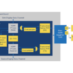
3.1. HDMI 2.0 RX-TX Retransmit Design Block Diagram
The HDMI 2.0 RX-TX retransmit design example demonstrates parallel loopback on simplex channel mode for HDMI Intel FPGA IP.
Figure 20. HDMI RX-TX Retransmit Block Diagram (Intel Quartus Prime Pro Edition) Figure 21. HDMI RX-TX Retransmit Block Diagram (Intel Quartus Prime Standard Edition)
 Related Information
Jitter of PLL Cascading or Non-Dedicated Clock Path for Arria 10 PLL Reference Clock Refer to this solution for workaround if your design clocks experience additional
jitter.
3.2. Hardware and Software Requirements
Intel uses the following hardware and software to test the design example.
Hardware
- Intel Arria 10 GX FPGA Development Kit
- HDMI Source (Graphics Processor Unit (GPU))
- HDMI Sink (Monitor)
- Bitec HDMI FMC 2.0 daughter card (Revision 11)
- HDMI cables
Note:
You can select the revision of your Bitec HDMI daughter card. Set the local parameter BITEC_DAUGHTER_CARD_REV to 4, 6, or 11 in the top-level file (a10_hdmi2_demo.v). When you change the revision, the design may swap the transceiver channels and invert the polarity according to the Bitec HDMI daughter cardrequirements. If you set the BITEC_DAUGHTER_CARD_REV parameter to 0, the design does not make any changes to the transceiver channels and the polarity. For HDMI 2.1 design examples, under the Design Example tab, set HDMI Daughter Card Revision to either Revision 9, Revision 4, or no daughter card. The default value is Revision 9.
Software
- Intel Quartus Prime version 18.1 and later (for hardware testing)
- ModelSim – Intel FPGA Edition, ModelSim – Intel FPGA Starter Edition, , RivieraPRO, VCS (Verilog HDL only)/VCS MX, or Xcelium Parallel simulator
3.3. Directory Structure
The directories contain the generated files for the HDMI Intel FPGA IP design example.
Figure 22. Directory Structure for the Design Example Table 30. Generated RTL Files
| Folders | Files |
| gxb | • /gxb_rx.qsys (Intel Quartus Prime Standard Edition) • /gxb_rx.ip (Intel Quartus Prime Pro Edition) |
| • /gxb_rx_reset.qsys (Intel Quartus Prime Standard Edition) • /gxb_rx_reset.ip (Intel Quartus Prime Pro Edition) |
|
| • /gxb_tx.qsys (Intel Quartus Prime Standard Edition) • /gxb_tx.ip (Intel Quartus Prime Pro Edition) |
|
| • /gxb_tx_fpll.qsys (Intel Quartus Prime Standard Edition) • /gxb_tx_fpll.ip (Intel Quartus Prime Pro Edition) |
|
| • /gxb_tx_reset.qsys (Intel Quartus Prime Standard Edition) • /gxb_tx_reset.ip (Intel Quartus Prime Pro Edition) |
|
| hdmi_rx | •/hdmi_rx.qsys (Intel Quartus Prime Standard Edition) •/hdmi_rx.ip (Intel Quartus Prime Pro Edition) |
| /hdmi_rx_top.v | |
| /mr_clock_sync.v (Intel Quartus Prime Standard Edition) | |
| /mr_hdmi_rx_core_top.v (Intel Quartus Prime Standard Edition) | |
| /mr_rx_oversample.v (Intel Quartus Prime Standard Edition) | |
| /symbol_aligner.v | |
| Panasonic.hex (Intel Quartus Prime Pro Edition) | |
| hdmi_tx | • /hdmi_tx.qsys (Intel Quartus Prime Standard Edition) •/hdmi_tx.ip (Intel Quartus Prime Pro Edition) |
| /hdmi_tx_top.v | |
| /mr_ce.v (Intel Quartus Prime Standard Edition) | |
| /mr_hdmi_tx_core_top.v (Intel Quartus Prime Standard Edition) | |
| /mr_tx_oversample.v (Intel Quartus Prime Standard Edition) | |
| i2c_master
(Intel Quartus Prime Standard Edition) |
/i2c_master_bit_ctrl.v |
| /i2c_master_byte_ctrl.v | |
| /i2c_master_defines.v | |
| /i2c_master_top.v | |
| /oc_i2c_master.v | |
| /oc_i2c_master_hw.tcl | |
| /timescale.v | |
| i2c_slave | /edid_ram.qsys (Intel Quartus Prime Standard Edition) |
| /Panasonic.hex (Intel Quartus Prime Standard Edition) | |
| /i2c_avl_mst_intf_gen.v | |
| /i2c_clk_cnt.v | |
| /i2c_condt_det.v | |
| /i2c_databuffer.v | |
| /i2c_rxshifter.v | |
| /i2c_slvfsm.v | |
| /i2c_spksupp.v | |
| /i2c_txout.v | |
| /i2c_txshifter.v | |
| /i2cslave_to_avlmm_bridge.v | |
| pll | • /pll_hdmi.qsys (Intel Quartus Prime Standard Edition) • /pll_hdmi.ip (Intel Quartus Prime Pro Edition) |
| • /pll_hdmi_reconfig.qsys (Intel Quartus Prime Standard Edition) • /pll_hdmi_reconfig.ip (Intel Quartus Prime Pro Edition) |
|
| quartus.ini | |
| common | • /clock_control.qsys (Intel Quartus Prime Standard Edition) • /clock_control.ip (Intel Quartus Prime Pro Edition) |
| • /fifo.qsys (Intel Quartus Prime Standard Edition) • /fifo.ip (Intel Quartus Prime Pro Edition) |
|
| • /output_buf_i2c.qsys (Intel Quartus Prime Standard Edition) •/output_buf_i2c.ip (Intel Quartus Prime Pro Edition) |
|
| /reset_controller.qsys (Intel Quartus Prime Standard Edition) | |
| /clock_crosser.v |
| dcfifo_inst.v | |
| debouncer.sv (Intel Quartus Prime Pro Edition) | |
| hdr | /altera_hdmi_aux_hdr.v |
| /altera_hdmi_aux_snk.v | |
| /altera_hdmi_aux_src.v | |
| /altera_hdmi_hdr_infoframe.v | |
| /avalon_st_mutiplexer.qsys | |
| reconfig_mgmt | /mr_compare_pll.v |
| /mr_compare_rx.v | |
| /mr_rate_detect.v | |
| /mr_reconfig_master_pll.v | |
| /mr_reconfig_master_rx.v | |
| /mr_reconfig_mgmt.v | |
| /mr_rom_pll_dprioaddr.v | |
| /mr_rom_pll_valuemask_8bpc.v | |
| /mr_rom_pll_valuemask_10bpc.v | |
| /mr_rom_pll_valuemask_12bpc.v | |
| /mr_rom_pll_valuemask_16bpc.v | |
| /mr_rom_rx_dprioaddr_bitmask.v | |
| /mr_rom_rx_valuemask.v | |
| /mr_state_machine.v | |
| sdc | /a10_hdmi2.sdc |
| /mr_reconfig_mgmt.sdc | |
| /jtag.sdc | |
| /rxtx_link.sdc | |
| /mr_clock_sync.sdc (Intel Quartus Prime Standard Edition) |
Table 31. Generated Simulation Files
Refer to the Simulation Testbench section for more information.
| Folders | Files |
| aldec | /aldec.do |
| /rivierapro_setup.tcl | |
| cadence | /cds.lib |
| /hdl.var | |
| <cds_libs folder> |
| mentor | /mentor.do |
| /msim_setup.tcl | |
| synopsys | /vcs/filelist.f |
| /vcs/vcs_setup.sh | |
| /vcs/vcs_sim.sh | |
| /vcsmx/vcsmx_setup.sh | |
| /vcsmx/vcsmx_sim.sh | |
| /vcsmx/synopsys_sim_setup | |
| xcelium
(Intel Quartus Prime Pro Edition) |
/cds.lib |
| /hdl.var | |
| /xcelium_setup.sh | |
| /xcelium_sim.sh | |
| <cds_libs folder> | |
| common
(Intel Quartus Prime Pro Edition) |
/modelsim_files.tcl |
| /riviera_files.tcl | |
| /vcs_files.tcl | |
| /vcsmx_files.tcl | |
| /xcelium_files.tcl | |
| hdmi_rx | • /hdmi_rx.qsys (Intel Quartus Prime Standard Edition) • /hdmi_rx.ip (Intel Quartus Prime Pro Edition) |
| /hdmi_rx.sopcinfo (Intel Quartus Prime Standard Edition) | |
| /Panasonic.hex (Intel Quartus Prime Pro Edition) | |
| /symbol_aligner.v (Intel Quartus Prime Pro Edition) | |
| hdmi_tx | • /hdmi_tx.qsys (Intel Quartus Prime Standard Edition) • /hdmi_tx.ip (Intel Quartus Prime Pro Edition) |
| /hdmi_tx.sopcinfo (Intel Quartus Prime Standard Edition) |
Table 32.Generated Software Files
| Folders | Files |
| tx_control_src Note: The tx_control folder also contains duplicates of these files. |
/intel_fpga_i2c.c (Intel Quartus Prime Pro Edition) |
| /intel_fpga_i2c.h (Intel Quartus Prime Pro Edition) | |
| /i2c.c (Intel Quartus Prime Standard Edition) | |
| /i2c.h (Intel Quartus Prime Standard Edition) | |
| /main.c | |
| /xcvr_gpll_rcfg.c /xcvr_gpll_rcfg.h /ti_i2c.c (Intel Quartus Prime Standard Edition) /ti_i2c.h (Intel Quartus Prime Standard Edition) |
3.4. Design Components
The HDMI Intel FPGA IP design example requires these components.
Table 33. HDMI RX Top Components
| Module |
Description |
| HDMI RX Core | The IP receives the serial data from the Transceiver Native PHY and performs data alignment, channel deskew, TMDS decoding, auxiliary data decoding, video data decoding, audio data decoding, and descrambling. |
| I2 | I2C is the interface used for Sink Display Data Channel (DDC) and Status and Data Channel (SCDC). The HDMI source uses the DDC to determine the capabilities and characteristics of the sink by reading the Enhanced Extended Display Identification Data (E-EDID) data structure. • The 8-bit I2C slave addresses for E-EDID are 0xA0 and 0xA1. The LSB indicates the access type: 1 for read and 0 for write. When an HPD event occurs, the I2C slave responds to E-EDID data by reading from the on-chip RAM. • The I2C slave-only controller also supports SCDC for HDMI 2.0 operations. The 8-bit I2C slave address for the SCDC are 0xA8 and 0xA9. When an HPD event occurs, the I2C slave performs write or read transaction to or from SCDC interface of the HDMI RX core. Note: This I2C slave-only controller for SCDC is not required if HDMI 2.0b is not intended. If you turn on the Include I2C parameter, this block will be included inside the core and will not be visible at this level. |
| EDID RAM | The design stores the EDID information using the RAM 1-port IP core. A standard two-wire (clock and data) serial bus protocol (I2C slave-only controller) transfers the CEA-861-D Compliant E-EDID data structure. This EDID RAM stores the E- EDID information. Note: If you turn on the Include EDID RAM parameter, this block will be included inside the core and will not be visible at this level. |
| IOPLL | The IOPLL generates the RX CDR reference clock, link speed clock, and video clock for the incoming TMDS clock. • Output clock 0 (CDR reference clock) • Output clock 1 (Link speed clock) • Output clock 2 (Video clock) Note: The default IOPLL configuration is not valid for any HDMI resolution. The IOPLL is reconfigured to the appropriate settings upon power up. |
| Transceiver PHY Reset Controller | The Transceiver PHY reset controller ensures a reliable initialization of the RX transceivers. The reset input of this controller is triggered by the RX reconfiguration, and it generates the corresponding analog and digital reset signal to the Transceiver Native PHY block according to the reset sequencing inside the block. |
| RX Native PHY | Hard transceiver block that receives the serial data from an external video source. It deserializes the serial data to parallel data before passing the data to the HDMI RX core. |
| RX Reconfiguration Management | RX reconfiguration management that implements rate detection circuitry with the HDMI PLL to drive the RX transceiver to operate at any arbitrary link rates ranging from 250 Mbps to 6,000 Mbps. Refer to Figure 23 on page 63 below. |
| IOPLL Reconfiguration | IOPLL reconfiguration block facilitates dynamic real-time reconfiguration of PLLs in Intel FPGAs. This block updates the output clock frequency and PLL bandwidth in real time, without reconfiguring the entire FPGA. This block runs at 100 MHz in Intel Arria 10 devices. Due to IOPLL reconfiguration limitation, apply the Quartus INI permit_nf_pll_reconfig_out_of_lock=on during the IOPLL reconfiguration IP generation. To apply the Quartus INI, include “permit_nf_pll_reconfig_out_of_lock=on” in the quartus.ini file and place in the file the Intel Quartus Prime project directory. You should see a warning message when you edit the IOPLL reconfiguration block (pll_hdmi_reconfig) in the Quartus Prime software with the INI. Note: Without this Quartus INI, IOPLL reconfiguration cannot be completed if the IOPLL loses lock during reconfiguration. |
| PIO | The parallel input/output (PIO) block functions as control, status and reset interfaces to or from the CPU sub-system. |
Figure 23. Multi-Rate Reconfiguration Sequence Flow
The figure illustrates the multi-rate reconfiguration sequence flow of the controller when it receives input data stream and reference clock frequency, or when the transceiver is unlocked. Table 34. HDMI TX Top Components
|
Module |
Description |
| HDMI TX Core | The IP core receives video data from the top level and performs TMDS encoding, auxiliary data encoding, audio data encoding, video data encoding, and scrambling. |
| I2C Master | I2C is the interface used for Sink Display Data Channel (DDC) and Status and Data Channel (SCDC). The HDMI source uses the DDC to determine the capabilities and characteristics of the sink by reading the Enhanced Extended Display Identification Data (E-EDID) data structure. • As DDC, I2C Master reads the EDID from the external sink to configure the EDID information EDID RAM in the HDMI RX Top or for video processing. • As SCDC, I2C master transfers the SCDC data structure from the FPGA source to the external sink for HDMI 2.0b operation. For example, if the outgoing data stream is above 3,400 Mbps, the Nios II processor commands the I2C master to update the TMDS_BIT_CLOCK_RATIO and SCRAMBLER_ENABLE bits of the sink SCDC configuration register to 1. |
| IOPLL | The IOPLL supplies the link speed clock and video clock from the incoming TMDS clock. • Output clock 1 (Link speed clock) • Output clock 2 (Video clock) Note: The default IOPLL configuration is not valid for any HDMI resolution. The IOPLL is reconfigured to the appropriate settings upon power up. |
| Transceiver PHY Reset Controller | The Transceiver PHY reset controller ensures a reliable initialization of the TX transceivers. The reset input of this controller is triggered from the top level, and it generates the corresponding analog and digital reset signal to the Transceiver Native PHY block according to the reset sequencing inside the block. The tx_ready output signal from this block also functions as a reset signal to the HDMI Intel FPGA IP to indicate the transceiver is up and running, and ready to receive data from the core. |
| Transceiver Native PHY | Hard transceiver block that receives the parallel data from the HDMI TX core and serializes the data from transmitting it. Reconfiguration interface is enabled in the TX Native PHY block to demonstrate the connection between TX Native PHY and transceiver arbiter. No reconfiguration is performed for TX Native PHY. Note: To meet the HDMI TX inter-channel skew requirement, set the TX channel bonding mode option in the Intel Arria 10 Transceiver Native PHY parameter editor to PMA and PCS bonding. You also need to add the maximum skew (set_max_skew) constraint requirement to the digital reset signal from the transceiver reset controller (tx_digitalreset) as recommended in the Intel Arria 10 Transceiver PHY User Guide. |
| TX PLL | The transmitter PLL block provides the serial fast clock to the Transceiver Native PHY block. For this HDMI Intel FPGA IP design example, fPLL is used as TX PLL. |
| IOPLL Reconfiguration | IOPLL reconfiguration block facilitates dynamic real-time reconfiguration of PLLs in Intel FPGAs. This block updates the output clock frequency and PLL bandwidth in real time, without reconfiguring the entire FPGA. This block runs at 100 MHz in Intel Arria 10 devices. Due to IOPLL reconfiguration limitation, apply the Quartus INI permit_nf_pll_reconfig_out_of_lock=on during the IOPLL reconfiguration IP generation. To apply the Quartus INI, include “permit_nf_pll_reconfig_out_of_lock=on” in the quartus.ini file and place in the file the Intel Quartus Prime project directory. You should see a warning message when you edit the IOPLL reconfiguration block (pll_hdmi_reconfig) in the Intel Quartus Prime software with the INI. Note: Without this Quartus INI, IOPLL reconfiguration cannot be completed if the IOPLL loses lock during reconfiguration. |
| PIO | The parallel input/output (PIO) block functions as control, status and reset interfaces to or from the CPU sub-system. |
Table 35. Transceiver Data Rate and Oversampling Factor for Each TMDS Clock Frequency Range
| TMDS Clock Frequency (MHz) | TMDS Bit clock Ratio | Oversampling Factor | Transceiver Data Rate (Mbps) |
| 85–150 | 1 | Not applicable | 3400–6000 |
| 100–340 | 0 | Not applicable | 1000–3400 |
| 50–100 | 0 | 5 | 2500–5000 |
| 35–50 | 0 | 3 | 1050–1500 |
| 30–35 | 0 | 4 | 1200–1400 |
| 25–30 | 0 | 5 | 1250–1500 |
Table 36. Top-Level Common Blocks
|
Module |
Description |
| Transceiver Arbiter | This generic functional block prevents transceivers from recalibrating simultaneously when either RX or TX transceivers within the same physical channel require reconfiguration. The simultaneous recalibration impacts applications where RX and TX transceivers within the same channel are assigned to independent IP implementations. This transceiver arbiter is an extension to the resolution recommended for merging simplex TX and simplex RX into the same physical channel. This transceiver arbiter also assists in merging and arbitrating the Avalon-MM RX and TX reconfiguration requests targeting simplex RX and TX transceivers within a channel as the reconfiguration interface port of the transceivers can only be accessed sequentially. The interface connection between the transceiver arbiter and TX/RX Native PHY/PHY Reset Controller blocks in this design example demonstrates a generic mode that apply for any IP combination using the transceiver arbiter. The transceiver arbiter is not required when only either RX or TX transceiver is used in a channel. The transceiver arbiter identifies the requester of a reconfiguration through its Avalon-MM reconfiguration interfaces and ensures that the corresponding tx_reconfig_cal_busy or rx_reconfig_cal_busy is gated accordingly. For HDMI application, only RX initiates reconfiguration. By channeling the Avalon-MM reconfiguration request through the arbiter, the arbiter identifies that the reconfiguration request originates from the RX, which then gates tx_reconfig_cal_busy from asserting and allows rx_reconfig_cal_busy to assert. The gating prevents the TX transceiver from being moved to calibration mode unintentionally. |
| Note: Because HDMI only requires RX reconfiguration, the tx_reconfig_mgmt_* signals are tied off. Also, the Avalon-MM interface is not required between the arbiter and the TX Native PHY block. The blocks are assigned to the interface in the design example to demonstrate generic transceiver arbiter connection to TX/RX Native PHY/PHY Reset Controller. | |
| RX-TX Link | • The video data output and synchronization signals from HDMI RX core loop through a DCFIFO across the RX and TX video clock domains. • The General Control Packet (GCP), InfoFrames (AVI, VSI and AI), auxiliary data, and audio data loop through DCFIFOs across the RX and TX link speed clock domains. • The auxiliary data port of the HDMI TX core controls the auxiliary data that flow through the DCFIFO through backpressure. The backpressure ensures there is no incomplete auxiliary packet on the auxiliary data port. • This block also performs external filtering: — Filters the audio data and audio clock regeneration packet from the auxiliary data stream before transmitting to the HDMI TX core auxiliary data port. Note: To disable this filtering, press user_pb[2]. Enable this filtering to ensure there is no duplication of audio data and audio clock regeneration packet in the retransmitted auxiliary data stream. — Filters the High Dynamic Range (HDR) InfoFrame from the HDMI RX auxiliary data and inserts an example HDR InfoFrame to the auxiliary data of the HDMI TX through the Avalon ST multiplexer. |
| CPU Sub-System | The CPU sub-system functions as SCDC and DDC controllers, and source reconfiguration controller. • The source SCDC controller contains the I2C master controller. The I2C master controller transfers the SCDC data structure from the FPGA source to the external sink for HDMI 2.0b operation. For example, if the outgoing data stream is 6,000 Mbps, the Nios II processor commands the I2C master controller to update the TMDS_BIT_CLOCK_RATIO and SCRAMBLER_ENABLE bits of the sink TMDS configuration register to 1. • The same I2C master also transfers the DDC data structure (E-EDID) between the HDMI source and external sink. • The Nios II CPU acts as the reconfiguration controller for the HDMI source. The CPU relies on the periodic rate detection from the RX Reconfiguration Management module to determine if the TX requires reconfiguration. The Avalon-MM slave translator provides the interface between the Nios II processor Avalon-MM master interface and the Avalon-MM slave interfaces of the externally instantiated HDMI source’s IOPLL and TX Native PHY. • The reconfiguration sequence flow for TX is same as RX, except that the PLL and transceiver reconfiguration and the reset sequence is performed sequentially. Refer to Figure 24 on page 67. |
Figure 24. Reconfiguration Sequence Flow
The figure illustrates the Nios II software flow that involves the controls for I2C master and HDMI source. 3.5. Dynamic Range and Mastering (HDR) InfoFrame Insertion and Filtering
The HDMI Intel FPGA IP design example includes a demonstration of HDR InfoFrame insertion in a RX-TX loopback system.
HDMI Specification version 2.0b allows Dynamic Range and Mastering InfoFrame to be transmitted through HDMI auxiliary stream. In the demonstration, the Auxiliary Data Insertion block supports the HDR insertion. You need only to format the intended HDR InfoFrame packet as specified in the module’s signal list table and use the provided AUX Insertion Control module to schedule the insertion of the HDR InfoFrame once every video frame.
In this example configuration, in instances where the incoming auxiliary stream already includes HDR InfoFrame, the streamed HDR content is filtered. The filtering avoids conflicting HDR InfoFrames to be transmitted and ensures that only the values specified in the HDR Sample Data module are used.
Figure 25. RX-TX Link with Dynamic Range and Mastering InfoFrame Insertion
The figure shows the block diagram of RX-TX link including Dynamic Range and Mastering InfoFrame insertion into the HDMI TX core auxiliary stream.
 Table 37. Auxiliary Data Insertion Block (altera_hdmi_aux_hdr) Signals
| Signal | Direction | Width |
Description |
| Clock and Reset | |||
| clk | Input | 1 | Clock input. This clock should be connected to the link speed clock. |
| reset | Input | 1 | Reset input. |
| Auxiliary Packet Generator and Multiplexer Signals | |||
| multiplexer_out_data | Output | 72 | Avalon streaming output from the multiplexer. |
| multiplexer_out_valid | Output | 1 | |
| multiplexer_out_ready | Output | 1 | |
| multiplexer_out_startofpacket | Output | 1 | |
| multiplexer_out_endofpacket | Output | 1 | |
| multiplexer_out_channel | Output | 11 | |
| multiplexer_in_data | Input | 72 | Avalon streaming input to the In1 port of the multiplexer. HDMI TX Video Vsync. This signal should be synchronized to the link speed clock domain. The core inserts the HDR InfoFrame to the auxiliary stream at the rising edge of this signal. |
| multiplexer_in_valid | Input | 1 | |
| multiplexer_in_ready | Input | 1 | |
| multiplexer_in_startofpacket | Input | 1 | |
| multiplexer_in_endofpacket hdmi_tx_vsync |
Input Input |
1 1 |
|
Table 38. HDR Data Module (altera_hdmi_hdr_infoframe) Signals
| Signal | Direction | Width |
Description |
| hb0 | Output | 8 | Header byte 0 of the Dynamic Range and Mastering InfoFrame: InfoFrame type code. |
| hb1 | Output | 8 | Header byte 1 of the Dynamic Range and Mastering InfoFrame: InfoFrame version number. |
| hb2 | Output | 8 | Header byte 2 of the Dynamic Range and Mastering InfoFrame: Length of InfoFrame. |
| pb | Input | 224 | Data byte of the Dynamic Range and Mastering InfoFrame. |
Table 39. Dynamic Range and Mastering InfoFrame Data Byte Bundle Bit-Fields
|
Bit-Field |
Definition |
Static Metadata Type 1 |
| 7:0 | Data Byte 1: {5’h0, EOTF[2:0]} | |
| 15:8 | Data Byte 2: {5’h0, Static_Metadata_Descriptor_ID[2:0]} | |
| 23:16 | Data Byte 3: Static_Metadata_Descriptor | display_primaries_x[0], LSB |
| 31:24 | Data Byte 4: Static_Metadata_Descriptor | display_primaries_x[0], MSB |
| 39:32 | Data Byte 5: Static_Metadata_Descriptor | display_primaries_y[0], LSB |
| 47:40 | Data Byte 6: Static_Metadata_Descriptor | display_primaries_y[0], MSB |
| 55:48 | Data Byte 7: Static_Metadata_Descriptor | display_primaries_x[1], LSB |
| 63:56 | Data Byte 8: Static_Metadata_Descriptor | display_primaries_x[1], MSB |
| 71:64 | Data Byte 9: Static_Metadata_Descriptor | display_primaries_y[1], LSB |
| 79:72 | Data Byte 10: Static_Metadata_Descriptor | display_primaries_y[1], MSB |
| 87:80 | Data Byte 11: Static_Metadata_Descriptor | display_primaries_x[2], LSB |
| 95:88 | Data Byte 12: Static_Metadata_Descriptor | display_primaries_x[2], MSB |
| 103:96 | Data Byte 13: Static_Metadata_Descriptor | display_primaries_y[2], LSB |
| 111:104 | Data Byte 14: Static_Metadata_Descriptor | display_primaries_y[2], MSB |
| 119:112 | Data Byte 15: Static_Metadata_Descriptor | white_point_x, LSB |
| 127:120 | Data Byte 16: Static_Metadata_Descriptor | white_point_x, MSB |
| 135:128 | Data Byte 17: Static_Metadata_Descriptor | white_point_y, LSB |
| 143:136 | Data Byte 18: Static_Metadata_Descriptor | white_point_y, MSB |
| 151:144 | Data Byte 19: Static_Metadata_Descriptor | max_display_mastering_luminance, LSB |
| 159:152 | Data Byte 20: Static_Metadata_Descriptor | max_display_mastering_luminance, MSB |
| 167:160 | Data Byte 21: Static_Metadata_Descriptor | min_display_mastering_luminance, LSB |
| 175:168 | Data Byte 22: Static_Metadata_Descriptor | min_display_mastering_luminance, MSB |
| 183:176 | Data Byte 23: Static_Metadata_Descriptor | Maximum Content Light Level, LSB |
| 191:184 | Data Byte 24: Static_Metadata_Descriptor | Maximum Content Light Level, MSB |
| 199:192 | Data Byte 25: Static_Metadata_Descriptor | Maximum Frame-average Light Level, LSB |
| 207:200 | Data Byte 26: Static_Metadata_Descriptor | Maximum Frame-average Light Level, MSB |
| 215:208 | Reserved | |
| 223:216 | Reserved | |
Disabling HDR Insertion and Filtering
Disabling HDR insertion and filter enables you to verify the retransmission of HDR content already available in the source auxiliary stream without any modification in the RX-TX Retransmit design example.
To disable HDR InfoFrame insertion and filtering:
- Set block_ext_hdr_infoframe to 1’b0 in the rxtx_link.v file to prevent the filtering of the HDR InfoFrame from the Auxiliary stream.
- Set multiplexer_in0_valid of the avalon_st_multiplexer instance in the altera_hdmi_aux_hdr.v file to 1’b0 to prevent the Auxiliary Packet Generator from forming and inserting additional HDR InfoFrame into the TX Auxiliary stream.
3.6. Clocking Scheme
The clocking scheme illustrates the clock domains in the HDMI Intel FPGA IP design example.
Figure 26. HDMI Intel FPGA IP Design Example Clocking Scheme (Intel Quartus Prime Pro Edition) Figure 27. HDMI Intel FPGA IP Design Example Clocking Scheme (Intel Quartus Prime Standard Edition)
 Table 40. Clocking Scheme Signals
| Clock | Signal Name in Design |
Description |
| TX IOPLL/ TX PLL Reference Clock 1 | hdmi_clk_in | Reference clock to the TX IOPLL and TX PLL. The clock frequency is the same as the expected TMDS clock frequency from the HDMI TX TMDS clock channel. For this HDMI Intel FPGA IP design example, this clock is connected to the RX TMDS clock for demonstration purpose. In your application, you need to supply a dedicated clock with TMDS clock frequency from a programmable oscillator for better jitter performance. Note: Do not use a transceiver RX pin as a TX PLL reference clock. Your design will fail to fit if you place the HDMI TX refclk on an RX pin. |
| TX Transceiver Clock Out | tx_clk | Clock out recovered from the transceiver, and the frequency varies depending on the data rate and symbols per clock. TX transceiver clock out frequency = Transceiver data rate/ (Symbol per clock*10) |
| TX PLL Serial Clock | tx_bonding_clocks | Serial fast clock generated by TX PLL. The clock frequency is set based on the data rate. |
| TX/RX Link Speed Clock | ls_clk | Link speed clock. The link speed clock frequency depends on the expected TMDS clock frequency, oversampling factor, symbols per clock, and TMDS bit clock ratio. |
| TMDS Bit Clock Ratio | Link Speed Clock Frequency | ||
| 0 | TMDS clock frequency/ Symbol per clock | ||
| 1 | TMDS clock frequency *4 / Symbol per clock | ||
| TX/RX Video Clock | vid_clk | Video data clock. The video data clock frequency is derived from the TX link speed clock based on the color depth. | |
| TMDS Bit Clock Ratio | Video Data Clock Frequency | ||
| 0 | TMDS clock/ Symbol per clock/ Color depth factor | ||
| 1 | TMDS clock *4 / Symbol per clock/ Color depth factor | ||
| Bits per Color | Color Depth Factor | ||
| 8 | 1 | ||
| 10 | 1.25 | ||
| 12 | 1.5 | ||
| 16 | 2.0 | ||
| RX TMDS Clock | tmds_clk_in | TMDS clock channel from the HDMI RX and connects to the reference clock to the IOPLL. | |
| RX CDR Reference Clock 0 /TX PLL Reference Clock 0 | fr_clk | Free running reference clock to RX CDR and TX PLL. This clock is required for power-up calibration. | |
| RX CDR Reference Clock 1 | iopll_outclk0 | Reference clock to the RX CDR of RX transceiver. | |
| Data Rate | RX Reference Clock Frequency | ||
| Data rate <1 Gbps | 5× TMDS clock frequency | ||
| 1 Gbps< Data rate
<3.4 Gbps |
TMDS clock frequency | ||
| Data rate >3.4 Gbps | 4× TMDS clock frequency | ||
| • Data Rate <1 Gbps: For oversampling to meet transceiver minimum data rate requirement. • Data Rate >3.4 Gbps: To compensate for the TMDS bit rate to clock ratio of 1/40 to maintain the transceiver data rate to clock ratio at 1/10. Note: Do not use a transceiver RX pin as a CDR reference clock. Your design will fail to fit if you place the HDMI RX refclk on an RX pin. |
|||
| RX Transceiver Clock Out | rx_clk | Clock out recovered from the transceiver, and the frequency varies depending on the data rate and symbols per clock.
RX transceiver clock out frequency = Transceiver data rate/ (Symbol per clock*10) |
|
| Management Clock | mgmt_clk | A free running 100 MHz clock for these components: | |
| • Avalon-MM interfaces for reconfiguration — The frequency range requirement is between 100– 125 MHz. •, PHY reset controller for transceiver reset sequence — The frequency range requirement is between 1–500 MHz. • IOPLL Reconfiguration — The maximum clock frequency is 100 MHz. • RX Reconfiguration for management • CPU • I2C Master |
||
| I2C Clock | i2c_clk | A 100 MHz clock input that clocks I2C slave, SCDC registers in the HDMI RX core, and EDID RAM. |
Related Information
- Using Transceiver RX Pin as CDR Reference Clock
- Using Transceiver RX Pin as TX PLL Reference Clock
3.7. Interface Signals
The tables list the signals for the HDMI Intel FPGA IP design example.
Table 41. Top-Level Signals
| Signal | Direction | Width |
Description |
| On-board Oscillator Signal | |||
| clk_fpga_b3_p | Input | 1 | 100 MHz free running clock for core reference clock |
| REFCLK_FMCB_P (Intel Quartus Prime Pro Edition) | Input | 1 | 625 MHz free running clock for transceiver reference clock; this clock can be of any frequency |
| User Push Buttons and LEDs | |||
| user_pb | Input | 1 | Push button to control the HDMI Intel FPGA IP design functionality |
| cpu_resetn | Input | 1 | Global reset |
| user_led_g | Output | 4 | Green LED display Refer to Hardware Setup on page 89 for more information about the LED functions. |
| user_led_r | Output | 4 | Red LED display Refer to Hardware Setup on page 89 for more information about the LED functions. |
| HDMI FMC Daughter Card Pins on FMC Port B | |||
| fmcb_gbtclk_m2c_p_0 | Input | 1 | HDMI RX TMDS clock |
| fmcb_dp_m2c_p | Input | 3 | HDMI RX red, green, and blue data channels • Bitec daughter card revision 11 — [0]: RX TMDS Channel 1 (Green) — [1]: RX TMDS Channel 2 (Red) — [2]: RX TMDS Channel 0 (Blue) • Bitec daughter card revision 4 or 6 — [0]: RX TMDS Channel 1 (Green)— polarity inverted — [1]: RX TMDS Channel 0 (Blue)— polarity inverted — [2]: RX TMDS Channel 2 (Red)— polarity inverted |
| fmcb_dp_c2m_p | Output | 4 | HDMI TX clock, red, green, and blue data channels • Bitec daughter card revision 11 — [0]: TX TMDS Channel 2 (Red) — [1]: TX TMDS Channel 1 (Green) — [2]: TX TMDS Channel 0 (Blue) — [3]: TX TMDS Clock Channel • Bitec daughter card revision 4 or 6 — [0]: TX TMDS Clock Channel — [1]: TX TMDS Channel 0 (Blue) — [2]: TX TMDS Channel 1 (Green) — [3]: TX TMDS Channel 2 (Red) |
| fmcb_la_rx_p_9 | Input | 1 | HDMI RX +5V power detect |
| fmcb_la_rx_p_8 | Inout | 1 | HDMI RX hot plug detect |
| fmcb_la_rx_n_8 | Inout | 1 | HDMI RX I2C SDA for DDC and SCDC |
| fmcb_la_tx_p_10 | Input | 1 | HDMI RX I2C SCL for DDC and SCDC |
| fmcb_la_tx_p_12 | Input | 1 | HDMI TX hot plug detect |
| fmcb_la_tx_n_12 | Inout | 1 | HDMI I2C SDA for DDC and SCDC |
| fmcb_la_rx_p_10 | Inout | 1 | HDMI I2C SCL for DDC and SCDC |
| fmcb_la_tx_p_11 | Inout | 1 | HDMI I2C SDA for redriver control |
| fmcb_la_rx_n_9 | Inout | 1 | HDMI I2C SCL for redriver control |
Table 42. HDMI RX Top-Level Signals
| Signal | Direction | Width |
Description |
| Clock and Reset Signals | |||
| mgmt_clk | Input | 1 | System clock input (100 MHz) |
| fr_clk (Intel Quartus Prime Pro Edition) | Input | 1 | Free running clock (625 MHz) for primary transceiver reference clock. This clock is required for transceiver calibration during power-up state. This clock can be of any frequency. |
| reset | Input | 1 | System reset input |
|
Signal |
Direction | Width |
Description |
| Clock and Reset Signals | |||
| reset_xcvr_powerup (Intel Quartus Prime Pro Edition) | Input | 1 | Transceiver reset input. This signal is asserted during the reference clocks switching process (from free running clock to TMDS clock) in power-up state. |
| tmds_clk_in | Input | 1 | HDMI RX TMDS clock |
| i2c_clk | Input | 1 | Clock input for DDC and SCDC interface |
| vid_clk_out | Output | 1 | Video clock output |
| ls_clk_out | Output | 1 | Link speed clock output |
| sys_init | Output | 1 | System initialization to reset the system upon power-up |
| RX Transceiver and IOPLL Signals | |||
| rx_serial_data | Input | 3 | HDMI serial data to the RX Native PHY |
| gxb_rx_ready | Output | 1 | Indicates RX Native PHY is ready |
| gxb_rx_cal_busy_out | Output | 3 | RX Native PHY calibration busy to the transceiver arbiter |
| gxb_rx_cal_busy_in | Input | 3 | Calibration busy signal from the transceiver arbiter to the RX Native PHY |
| iopll_locked | Output | 1 | Indicate IOPLL is locked |
| gxb_reconfig_write | Input | 3 | Transceiver reconfiguration Avalon-MM interface from the RX Native PHY to the transceiver arbiter |
| gxb_reconfig_read | Input | 3 | |
| gxb_reconfig_address | Input | 30 | |
| gxb_reconfig_writedata | Input | 96 | |
| gxb_reconfig_readdata | Output | 96 | |
| gxb_reconfig_waitrequest | Output | 3 | |
| RX Reconfiguration Management | |||
| rx_reconfig_en | Output | 1 | RX Reconfiguration enables signal |
| measure | Output | 24 | HDMI RX TMDS clock frequency measurement (in 10 ms) |
| measure_valid | Output | 1 | Indicates the measure signal is valid |
| os | Output | 1 | Oversampling factor: • 0: No oversampling • 1: 5× oversampling |
| reconfig_mgmt_write | Output | 1 | RX reconfiguration management Avalon memory-mapped interface to transceiver arbiter |
| reconfig_mgmt_read | Output | 1 | |
| reconfig_mgmt_address | Output | 12 | |
| reconfig_mgmt_writedata | Output | 32 | |
| reconfig_mgmt_readdata | Input | 32 | |
| reconfig_mgmt_waitrequest | Input | 1 |
| HDMI RX Core Signals | |||
| TMDS_Bit_clock_Ratio | Output | 1 | SCDC register interfaces |
| audio_de | Output | 1 | HDMI RX core audio interfaces Refer to the Sink Interfaces section in the HDMI Intel FPGA IP User Guide for more information. |
| audio_data | Output | 256 | |
| audio_info_ai | Output | 48 | |
| audio_N | Output | 20 | |
| audio_CTS | Output | 20 | |
| audio_metadata | Output | 165 | |
| audio_format | Output | 5 | |
| aux_pkt_data | Output | 72 | HDMI RX core auxiliary interfaces Refer to the Sink Interfaces section in the HDMI Intel FPGA IP User Guide for more information. |
| aux_pkt_addr | Output | 6 | |
| aux_pkt_wr | Output | 1 | |
| aux_data | Output | 72 | |
| aux_sop | Output | 1 | |
| aux_eop | Output | 1 | |
| aux_valid | Output | 1 | |
| aux_error | Output | 1 | |
| gcp | Output | 6 | HDMI RX core sideband signals Refer to the Sink Interfaces section in the HDMI Intel FPGA IP User Guide for more information. |
| info_avi | Output | 112 | |
| info_vsi | Output | 61 | |
| colordepth_mgmt_sync | Output | 2 | |
| vid_data | Output | N*48 | HDMI RX core video ports Note: N = symbols per clock Refer to the Sink Interfaces section in the HDMI Intel FPGA IP User Guide for more information. |
| vid_vsync | Output | N | |
| vid_hsync | Output | N | |
| vid_de | Output | N | |
| mode | Output | 1 | HDMI RX core control and status ports Note: N = symbols per clock Refer to the Sink Interfaces section in the HDMI Intel FPGA IP User Guide for more information. |
| ctrl | Output | N*6 | |
| locked | Output | 3 | |
| vid_lock | Output | 1 | |
| in_5v_power | Input | 1 | HDMI RX 5V detect and hotplug detect Refer to the Sink Interfaces section in the HDMI Intel FPGA IP User Guide for more information. |
| hdmi_rx_hpd_n | Inout | 1 | |
| hdmi_rx_i2c_sda | Inout | 1 | HDMI RX DDC and SCDC interface |
| hdmi_rx_i2c_scl | Inout | 1 |
| RX EDID RAM Signals | |||
| edid_ram_access | Input | 1 | HDMI RX EDID RAM access interface. Assert edid_ram_access when you want to write or read from the EDID RAM, else this signal should be kept low. |
| edid_ram_address | Input | 8 | |
| edid_ram_write | Input | 1 | |
| edid_ram_read | Input | 1 | |
| edid_ram_readdata | Output | 8 | |
| edid_ram_writedata | Input | 8 | |
| edid_ram_waitrequest | Output | 1 | |
Table 43. HDMI TX Top-Level Signals
| Signal | Direction | Width | Description |
| Clock and Reset Signals | |||
| mgmt_clk | Input | 1 | System clock input (100 MHz) |
| fr_clk (Intel Quartus Prime Pro Edition) | Input | 1 | Free running clock (625 MHz) for primary transceiver reference clock. This clock is required for transceiver calibration during power-up state. This clock can be of any frequency. |
| reset | Input | 1 | System reset input |
| hdmi_clk_in | Input | 1 | Reference clock to TX IOPLL and TX PLL. The clock frequency is the same as the TMDS clock frequency. |
| vid_clk_out | Output | 1 | Video clock output |
| ls_clk_out | Output | 1 | Link speed clock output |
| sys_init | Output | 1 | System initialization to reset the system upon power-up |
| reset_xcvr | Input | 1 | Reset to TX transceiver |
| reset_pll | Input | 1 | Reset to IOPLL and TX PLL |
| reset_pll_reconfig | Output | 1 | Reset to PLL reconfiguration |
| TX Transceiver and IOPLL Signals | |||
| tx_serial_data | Output | 4 | HDMI serial data from the TX Native PHY |
| gxb_tx_ready | Output | 1 | Indicates TX Native PHY is ready |
| gxb_tx_cal_busy_out | Output | 4 | TX Native PHY calibration busy signal to the transceiver arbiter |
| gxb_tx_cal_busy_in | Input | 4 | Calibration busy signal from the transceiver arbiter to the TX Native PHY |
| TX Transceiver and IOPLL Signals | |||
| iopll_locked | Output | 1 | Indicate IOPLL is locked |
| txpll_locked | Output | 1 | Indicate TX PLL is locked |
| gxb_reconfig_write | Input | 4 | Transceiver reconfiguration Avalon memory-mapped interface from the TX Native PHY to the transceiver arbiter |
| gxb_reconfig_read | Input | 4 | |
| gxb_reconfig_address | Input | 40 | |
| gxb_reconfig_writedata | Input | 128 | |
| gxb_reconfig_readdata | Output | 128 | |
| gxb_reconfig_waitrequest | Output | 4 | |
| TX IOPLL and TX PLL Reconfiguration Signals | |||
| pll_reconfig_write/ tx_pll_reconfig_write | Input | 1 | TX IOPLL/TX PLL reconfiguration Avalon memory-mapped interfaces |
| pll_reconfig_read/ tx_pll_reconfig_read | Input | 1 | |
| pll_reconfig_address/ tx_pll_reconfig_address | Input | 10 | |
| pll_reconfig_writedata/ tx_pll_reconfig_writedata | Input | 32 | |
| pll_reconfig_readdata/ tx_pll_reconfig_readdata | Output | 32 | |
| pll_reconfig_waitrequest/ tx_pll_reconfig_waitrequest | Output | 1 | |
| os | Input | 2 | Oversampling factor: • 0: No oversampling • 1: 3× oversampling • 2: 4× oversampling • 3: 5× oversampling |
| measure | Input | 24 | Indicates the TMDS clock frequency of the transmitting video resolution. |
| HDMI TX Core Signals | |||
| ctrl | Input | 6*N | HDMI TX core control interfaces Note: N = Symbols per clock Refer to the Source Interfaces section in the HDMI Intel FPGA IP User Guide for more information. |
| mode | Input | 1 | |
| TMDS_Bit_clock_Ratio | Input | 1 | SCDC register interfaces
Refer to the Source Interfaces section in the HDMI Intel FPGA IP User Guide for more information. |
| Scrambler_Enable | Input | 1 | |
| audio_de | Input | 1 | HDMI TX core audio interfaces
Refer to the Source Interfaces section in the HDMI Intel FPGA IP User Guide for more information. |
| audio_mute | Input | 1 | |
| audio_data | Input | 256 | |
| continued… | |||
| HDMI TX Core Signals | |||
| audio_info_ai | Input | 49 | |
| audio_N | Input | 22 | |
| audio_CTS | Input | 22 | |
| audio_metadata | Input | 166 | |
| audio_format | Input | 5 | |
| i2c_master_write | Input | 1 | TX I2C master Avalon memory-mapped interface to I2C master inside the TX core. Note: These signals are available only when you turn on the Include I2C parameter. |
| i2c_master_read | Input | 1 | |
| i2c_master_address | Input | 4 | |
| i2c_master_writedata | Input | 32 | |
| i2c_master_readdata | Output | 32 | |
| aux_ready | Output | 1 | HDMI TX core auxiliary interfaces
Refer to the Source Interfaces section in the HDMI Intel FPGA IP User Guide for more information. |
| aux_data | Input | 72 | |
| aux_sop | Input | 1 | |
| aux_eop | Input | 1 | |
| aux_valid | Input | 1 | |
| gcp | Input | 6 | HDMI TX core sideband signals Refer to the Source Interfaces section in the HDMI Intel FPGA IP User Guide for more information. |
| info_avi | Input | 113 | |
| info_vsi | Input | 62 | |
| vid_data | Input | N*48 | HDMI TX core video ports Note: N = symbols per clock Refer to the Source Interfaces section in the HDMI Intel FPGA IP User Guide for more information. |
| vid_vsync | Input | N | |
| vid_hsync | Input | N | |
| vid_de | Input | N | |
| I2C and Hot Plug Detect Signals | |||
| nios_tx_i2c_sda_in (Intel Quartus Prime Pro Edition) Note: When you turn on the Include I2C parameter, this signal is placed in the TX core and will not be visible at this level. |
Output | 1 | I2C Master Avalon memory-mapped interfaces |
| nios_tx_i2c_scl_in (Intel Quartus Prime Pro Edition) Note: When you turn on the Include I2C parameter, this signal is placed in the TX core and will not be visible at this level. |
Output | 1 | |
| nios_tx_i2c_sda_oe (Intel Quartus Prime Pro Edition) Note: When you turn on the Include I2C parameter, this signal is placed in the TX core and will not be visible at this level. |
Input | 1 | |
| continued… | |||
| I2C and Hot Plug Detect Signals | |||
| nios_tx_i2c_scl_oe (Intel Quartus Prime Pro Edition) Note: When you turn on the Include I2C parameter, this signal is placed in the TX core and will not be visible at this level. |
Input | 1 | |
| nios_ti_i2c_sda_in (Intel Quartus Prime Pro Edition) | Output | 1 | |
| nios_ti_i2c_scl_in (Intel Quartus Prime Pro Edition) | Output | 1 | |
| nios_ti_i2c_sda_oe (Intel Quartus Prime Pro Edition) | Input | 1 | |
| nios_ti_i2c_scl_oe (Intel Quartus Prime Pro Edition) | Input | 1 | |
| hdmi_tx_i2c_sda | Inout | 1 | HDMI TX DDC and SCDC interfaces |
| hdmi_tx_i2c_scl | Inout | 1 | |
| hdmi_ti_i2c_sda (Intel Quartus Prime Pro Edition) | Inout | 1 | I2C interface for Bitec Daughter Card Revision 11 TI181 Control |
| hdmi_tx_ti_i2c_sda (Intel Quartus Prime Standard Edition) | Inout | 1 | |
| hdmi_ti_i2c_scl (Intel Quartus Prime Pro Edition) | Inout | 1 | |
| hdmi_tx_ti_i2c_scl (Intel Quartus Prime Standard Edition) | Inout | 1 | |
| tx_i2c_avalon_waitrequest | Output | 1 | Avalon memory-mapped interfaces of I2C master |
| tx_i2c_avalon_address (Intel Quartus Prime Standard Edition) | Input | 3 | |
| tx_i2c_avalon_writedata (Intel Quartus Prime Standard Edition) | Input | 8 | |
| tx_i2c_avalon_readdata (Intel Quartus Prime Standard Edition) | Output | 8 | |
| tx_i2c_avalon_chipselect (Intel Quartus Prime Standard Edition) | Input | 1 | |
| tx_i2c_avalon_write (Intel Quartus Prime Standard Edition) | Input | 1 | |
| tx_i2c_irq (Intel Quartus Prime Standard Edition) | Output | 1 | |
| tx_ti_i2c_avalon_waitrequest
(Intel Quartus Prime Standard Edition) |
Output | 1 | |
| tx_ti_i2c_avalon_address (Intel Quartus Prime Standard Edition) | Input | 3 | |
| tx_ti_i2c_avalon_writedata (Intel Quartus Prime Standard Edition) | Input | 8 | |
| tx_ti_i2c_avalon_readdata (Intel Quartus Prime Standard Edition) | Output | 8 | |
| continued… | |||
| I2C and Hot Plug Detect Signals | |||
| tx_ti_i2c_avalon_chipselect (Intel Quartus Prime Standard Edition) | Input | 1 | |
| tx_ti_i2c_avalon_write (Intel Quartus Prime Standard Edition) | Input | 1 | |
| tx_ti_i2c_irq (Intel Quartus Prime Standard Edition) | Output | 1 | |
| hdmi_tx_hpd_n | Input | 1 | HDMI TX hotplug detect interfaces |
| tx_hpd_ack | Input | 1 | |
| tx_hpd_req | Output | 1 | |
Table 44. Transceiver Arbiter Signals
| Signal | Direction | Width | Description |
| clk | Input | 1 | Reconfiguration clock. This clock must share the same clock with the reconfiguration management blocks. |
| reset | Input | 1 | Reset signal. This reset must share the same reset with the reconfiguration management blocks. |
| rx_rcfg_en | Input | 1 | RX reconfiguration enable signal |
| tx_rcfg_en | Input | 1 | TX reconfiguration enable signal |
| rx_rcfg_ch | Input | 2 | Indicates which channel to be reconfigured on the RX core. This signal must always remain asserted. |
| tx_rcfg_ch | Input | 2 | Indicates which channel to be reconfigured on the TX core. This signal must always remain asserted. |
| rx_reconfig_mgmt_write | Input | 1 | Reconfiguration Avalon-MM interfaces from the RX reconfiguration management |
| rx_reconfig_mgmt_read | Input | 1 | |
| rx_reconfig_mgmt_address | Input | 10 | |
| rx_reconfig_mgmt_writedata | Input | 32 | |
| rx_reconfig_mgmt_readdata | Output | 32 | |
| rx_reconfig_mgmt_waitrequest | Output | 1 | |
| tx_reconfig_mgmt_write | Input | 1 | Reconfiguration Avalon-MM interfaces from the TX reconfiguration management |
| tx_reconfig_mgmt_read | Input | 1 | |
| tx_reconfig_mgmt_address | Input | 10 | |
| tx_reconfig_mgmt_writedata | Input | 32 | |
| tx_reconfig_mgmt_readdata | Output | 32 | |
| tx_reconfig_mgmt_waitrequest | Output | 1 | |
| reconfig_write | Output | 1 | Reconfiguration Avalon-MM interfaces to the transceiver |
| reconfig_read | Output | 1 | |
| continued… | |||
| Signal | Direction | Width | Description |
| reconfig_address | Output | 10 | |
| reconfig_writedata | Output | 32 | |
| rx_reconfig_readdata | Input | 32 | |
| rx_reconfig_waitrequest | Input | 1 | |
| tx_reconfig_readdata | Input | 1 | |
| tx_reconfig_waitrequest | Input | 1 | |
| rx_cal_busy | Input | 1 | Calibration status signal from the RX transceiver |
| tx_cal_busy | Input | 1 | Calibration status signal from the TX transceiver |
| rx_reconfig_cal_busy | Output | 1 | Calibration status signal to the RX transceiver PHY reset control |
| tx_reconfig_cal_busy | Output | 1 | Calibration status signal from the TX transceiver PHY reset control |
Table 45. RX-TX Link Signals
| Signal | Direction | Width | Description |
| reset | Input | 1 | Reset to the video/audio/auxiliary/ sidebands FIFO buffer. |
| hdmi_tx_ls_clk | Input | 1 | HDMI TX link speed clock |
| hdmi_rx_ls_clk | Input | 1 | HDMI RX link speed clock |
| hdmi_tx_vid_clk | Input | 1 | HDMI TX video clock |
| hdmi_rx_vid_clk | Input | 1 | HDMI RX video clock |
| hdmi_rx_locked | Input | 3 | Indicates HDMI RX locked status |
| hdmi_rx_de | Input | N | HDMI RX video interfaces Note: N = symbols per clock |
| hdmi_rx_hsync | Input | N | |
| hdmi_rx_vsync | Input | N | |
| hdmi_rx_data | Input | N*48 | |
| rx_audio_format | Input | 5 | HDMI RX audio interfaces |
| rx_audio_metadata | Input | 165 | |
| rx_audio_info_ai | Input | 48 | |
| rx_audio_CTS | Input | 20 | |
| rx_audio_N | Input | 20 | |
| rx_audio_de | Input | 1 | |
| rx_audio_data | Input | 256 | |
| rx_gcp | Input | 6 | HDMI RX sideband interfaces |
| rx_info_avi | Input | 112 | |
| rx_info_vsi | Input | 61 | |
| continued… | |||
| Signal | Direction | Width | Description |
| rx_aux_eop | Input | 1 | HDMI RX auxiliary interfaces |
| rx_aux_sop | Input | 1 | |
| rx_aux_valid | Input | 1 | |
| rx_aux_data | Input | 72 | |
| hdmi_tx_de | Output | N | HDMI TX video interfaces
Note: N = symbols per clock |
| hdmi_tx_hsync | Output | N | |
| hdmi_tx_vsync | Output | N | |
| hdmi_tx_data | Output | N*48 | |
| tx_audio_format | Output | 5 | HDMI TX audio interfaces |
| tx_audio_metadata | Output | 165 | |
| tx_audio_info_ai | Output | 48 | |
| tx_audio_CTS | Output | 20 | |
| tx_audio_N | Output | 20 | |
| tx_audio_de | Output | 1 | |
| tx_audio_data | Output | 256 | |
| tx_gcp | Output | 6 | HDMI TX sideband interfaces |
| tx_info_avi | Output | 112 | |
| tx_info_vsi | Output | 61 | |
| tx_aux_eop | Output | 1 | HDMI TX auxiliary interfaces |
| tx_aux_sop | Output | 1 | |
| tx_aux_valid | Output | 1 | |
| tx_aux_data | Output | 72 | |
| tx_aux_ready | Output | 1 |
Table 46. Platform Designer System Signals
| Signal | Direction | Width | Description |
| cpu_clk (Intel Quartus Prime Standard Edition) | Input | 1 | CPU clock |
| clock_bridge_0_in_clk_clk (Intel Quartus Prime Pro Edition) | |||
| cpu_clk_reset_n (Intel Quartus Prime Standard Edition) | Input | 1 | CPU reset |
| reset_bridge_0_reset_reset_n (Intel Quartus Prime Pro Edition) | |||
| tmds_bit_clock_ratio_pio_external_connectio n_export | Input | 1 | TMDS bit clock ratio |
| measure_pio_external_connection_export | Input | 24 | Expected TMDS clock frequency |
| continued… | |||
| Signal | Direction | Width | Description |
| measure_valid_pio_external_connection_expor t | Input | 1 | Indicates measure PIO is valid |
| i2c_master_i2c_serial_sda_in (Intel Quartus Prime Pro Edition) | Input | 1 | I2C Master interfaces |
| i2c_master_i2c_serial_scl_in (Intel Quartus Prime Pro Edition) | Input | 1 | |
| i2c_master_i2c_serial_sda_oe (Intel Quartus Prime Pro Edition) | Output | 1 | |
| i2c_master_i2c_serial_scl_oe (Intel Quartus Prime Pro Edition) | Output | 1 | |
| i2c_master_ti_i2c_serial_sda_in (Intel Quartus Prime Pro Edition) | Input | 1 | |
| i2c_master_ti_i2c_serial_scl_in (Intel Quartus Prime Pro Edition) | Input | 1 | |
| i2c_master_ti_i2c_serial_sda_oe (Intel Quartus Prime Pro Edition) | Output | 1 | |
| i2c_master_ti_i2c_serial_scl_oe (Intel Quartus Prime Pro Edition) | Output | 1 | |
| oc_i2c_master_av_slave_translator_avalon_an ti_slave_0_address (Intel Quartus Prime Pro Edition) | Output | 3 | I2C Master Avalon memory-mapped interfaces for DDC and SCDC |
| oc_i2c_master_av_slave_translator_avalon_an ti_slave_0_write (Intel Quartus Prime Pro Edition) | Output | 1 | |
| oc_i2c_master_av_slave_translator_avalon_an ti_slave_0_readdata (Intel Quartus Prime Pro Edition) | Input | 32 | |
| oc_i2c_master_av_slave_translator_avalon_an ti_slave_0_writedata (Intel Quartus Prime Pro Edition) | Output | 32 | |
| oc_i2c_master_av_slave_translator_avalon_an ti_slave_0_waitrequest (Intel Quartus Prime Pro Edition) | Input | 1 | |
| oc_i2c_master_av_slave_translator_avalon_an ti_slave_0_chipselect (Intel Quartus Prime Pro Edition) | Output | 1 | |
| oc_i2c_master_ti_avalon_anti_slave_address (Intel Quartus Prime Standard Edition) | Output | 3 | I2C Master Avalon memory-mapped interfaces for Bitec daughter card revision 11, T1181 control |
| oc_i2c_master_ti_avalon_anti_slave_write (Intel Quartus Prime Standard Edition) | Output | 1 | |
| oc_i2c_master_ti_avalon_anti_slave_readdata (Intel Quartus Prime Standard Edition) | Input | 32 | |
| oc_i2c_master_ti_avalon_anti_slave_writedat a (Intel Quartus Prime Standard Edition) | Output | 32 | |
| oc_i2c_master_ti_avalon_anti_slave_waitrequ est (Intel Quartus Prime Standard Edition) | Input | 1 | |
| oc_i2c_master_ti_avalon_anti_slave_chipsele ct (Intel Quartus Prime Standard Edition) | Output | 1 | |
| continued… | |||
| Signal | Direction | Width | Description |
| edid_ram_access_pio_external_connection_exp ort | Output | 1 | EDID RAM access interfaces. Assert edid_ram_access_pio_ external_connection_ export when you want to write to or read from the EDID RAM on the RX top. Connect EDID RAM access Avalon-MM slave in Platform Designer to the EDID RAM interface on the top-level RX modules. |
| edid_ram_slave_translator_address | Output | 8 | |
| edid_ram_slave_translator_write | Output | 1 | |
| edid_ram_slave_translator_read | Output | 1 | |
| edid_ram_slave_translator_readdata | Input | 8 | |
| edid_ram_slave_translator_writedata | Output | 8 | |
| edid_ram_slave_translator_waitrequest | Input | 1 | |
| powerup_cal_done_export (Intel Quartus Prime Pro Edition) | Input | 1 | RX PMA Reconfiguration Avalon memory-mapped interfaces |
| rx_pma_cal_busy_export (Intel Quartus Prime Pro Edition) | Input | 1 | |
| rx_pma_ch_export (Intel Quartus Prime Pro Edition) | Output | 2 | |
| rx_pma_rcfg_mgmt_address (Intel Quartus Prime Pro Edition) | Output | 12 | |
| rx_pma_rcfg_mgmt_write (Intel Quartus Prime Pro Edition) | Output | 1 | |
| rx_pma_rcfg_mgmt_read (Intel Quartus Prime Pro Edition) | Output | 1 | |
| rx_pma_rcfg_mgmt_readdata (Intel Quartus Prime Pro Edition) | Input | 32 | |
| rx_pma_rcfg_mgmt_writedata (Intel Quartus Prime Pro Edition) | Output | 32 | |
| rx_pma_rcfg_mgmt_waitrequest (Intel Quartus Prime Pro Edition) | Input | 1 | |
| rx_pma_waitrequest_export (Intel Quartus Prime Pro Edition) | Input | 1 | |
| rx_rcfg_en_export (Intel Quartus Prime Pro Edition) | Output | 1 | |
| rx_rst_xcvr_export (Intel Quartus Prime Pro Edition) | Output | 1 | |
| tx_pll_rcfg_mgmt_translator_avalon_anti_sla ve_waitrequest | Input | 1 | TX PLL Reconfiguration Avalon memory-mapped interfaces |
| tx_pll_rcfg_mgmt_translator_avalon_anti_sla ve_writedata | Output | 32 | |
| tx_pll_rcfg_mgmt_translator_avalon_anti_sla ve_address | Output | 10 | |
| tx_pll_rcfg_mgmt_translator_avalon_anti_sla ve_write | Output | 1 | |
| tx_pll_rcfg_mgmt_translator_avalon_anti_sla ve_read | Output | 1 | |
| tx_pll_rcfg_mgmt_translator_avalon_anti_sla ve_readdata | Input | 32 | |
| continued… | |||
| Signal | Direction | Width | Description |
| tx_pll_waitrequest_pio_external_connection_ export | Input | 1 | TX PLL waitrequest |
| tx_pma_rcfg_mgmt_translator_avalon_anti_sla ve_address | Output | 12 | TX PMA Reconfiguration Avalon memory-mapped interfaces |
| tx_pma_rcfg_mgmt_translator_avalon_anti_sla ve_write | Output | 1 | |
| tx_pma_rcfg_mgmt_translator_avalon_anti_sla ve_read | Output | 1 | |
| tx_pma_rcfg_mgmt_translator_avalon_anti_sla ve_readdata | Input | 32 | |
| tx_pma_rcfg_mgmt_translator_avalon_anti_sla ve_writedata | Output | 32 | |
| tx_pma_rcfg_mgmt_translator_avalon_anti_sla ve_waitrequest | Input | 1 | |
| tx_pma_waitrequest_pio_external_connection_ export | Input | 1 | TX PMA waitrequest |
| tx_pma_cal_busy_pio_external_connection_exp ort | Input | 1 | TX PMA Recalibration Busy |
| tx_pma_ch_export | Output | 2 | TX PMA Channels |
| tx_rcfg_en_pio_external_connection_export | Output | 1 | TX PMA Reconfiguration Enable |
| tx_iopll_rcfg_mgmt_translator_avalon_anti_s lave_writedata | Output | 32 | TX IOPLL Reconfiguration Avalon memory-mapped interfaces |
| tx_iopll_rcfg_mgmt_translator_avalon_anti_s lave_readdata | Input | 32 | |
| tx_iopll_rcfg_mgmt_translator_avalon_anti_s lave_waitrequest | Input | 1 | |
| tx_iopll_rcfg_mgmt_translator_avalon_anti_s lave_address | Output | 9 | |
| tx_iopll_rcfg_mgmt_translator_avalon_anti_s lave_write | Output | 1 | |
| tx_iopll_rcfg_mgmt_translator_avalon_anti_s lave_read | Output | 1 | |
| tx_os_pio_external_connection_export | Output | 2 | Oversampling factor: • 0: No oversampling • 1: 3× oversampling • 2: 4× oversampling • 3: 5× oversampling |
| tx_rst_pll_pio_external_connection_export | Output | 1 | Reset to IOPLL and TX PLL |
| tx_rst_xcvr_pio_external_connection_export | Output | 1 | Reset to TX Native PHY |
| wd_timer_resetrequest_reset | Output | 1 | Watchdog timer reset |
| color_depth_pio_external_connection_export | Input | 2 | Color depth |
| tx_hpd_ack_pio_external_connection_export | Output | 1 | For TX hotplug detect handshaking |
| tx_hpd_req_pio_external_connection_export | Input | 1 |
3.8. Design RTL Parameters
Use the HDMI TX and RX Top RTL parameters to customize the design example.
Most of the design parameters are available in the Design Example tab of the HDMI Intel FPGA IP parameter editor. You can still change the design example settings you
made in the parameter editor through the RTL parameters.
Table 47. HDMI RX Top Parameters
| Parameter | Value | Description |
| SUPPORT_DEEP_COLOR | • 0: No deep color • 1: Deep color |
Determines if the core can encode deep color formats. |
| SUPPORT_AUXILIARY | • 0: No AUX • 1: AUX |
Determines if the auxiliary channel encoding is included. |
| SYMBOLS_PER_CLOCK | 8 | Supports 8 symbols per clock for Intel Arria 10 devices. |
| SUPPORT_AUDIO | • 0: No audio • 1: Audio |
Determines if the core can encode audio. |
| EDID_RAM_ADDR_WIDTH (Intel Quartus Prime Standard Edition) | 8 (Default value) | Log base 2 of the EDID RAM size. |
| BITEC_DAUGHTER_CARD_REV | • 0: Not targeting any Bitec HDMI daughter card • 4: Supports Bitec HDMI daughter card revision 4 • 6: Targeting Bitec HDMI daughter card revision 6 •11: Targeting Bitec HDMI daughter card revision 11 (default) |
Specifies the revision of the Bitec HDMI daughter card used. When you change the revision, the design may swap the transceiver channels and invert the polarity according to the Bitec HDMI daughter card requirements. If you set the BITEC_DAUGHTER_CARD_REV parameter to 0, the design does not make any changes to the transceiver channels and the polarity. |
| POLARITY_INVERSION | • 0: Invert polarity • 1: Do not invert polarity |
Set this parameter to 1 to invert the value of each bit of the input data. Setting this parameter to 1 assigns 4’b1111 to the rx_polinv port of the RX transceiver. |
Table 48. HDMI TX Top Parameters
| Parameter | Value | Description |
| USE_FPLL | 1 | Supports fPLL as TX PLL only for Intel Cyclone® 10 GX devices. Always set this parameter to 1. |
| SUPPORT_DEEP_COLOR | • 0: No deep color • 1: Deep color |
Determines if the core can encode deep color formats. |
| SUPPORT_AUXILIARY | • 0: No AUX • 1: AUX |
Determines if the auxiliary channel encoding is included. |
| SYMBOLS_PER_CLOCK | 8 | Supports 8 symbols per clock for Intel Arria 10 devices. |
| continued… | ||
| Parameter | Value | Description |
| SUPPORT_AUDIO | • 0: No audio • 1: Audio |
Determines if the core can encode audio. |
| BITEC_DAUGHTER_CARD_REV | • 0: Not targeting any Bitec HDMI daughter card • 4: Supports Bitec HDMI daughter card revision 4 • 6: Targeting Bitec HDMI daughter card revision 6 • 11: Targeting Bitec HDMI daughter card revision 11 (default) |
Specifies the revision of the Bitec HDMI daughter card used. When you change the revision, the design may swap the transceiver channels and invert the polarity according to the Bitec HDMI daughter card requirements. If you set the BITEC_DAUGHTER_CARD_REV parameter to 0, the design does not make any changes to the transceiver channels and the polarity. |
| POLARITY_INVERSION | • 0: Invert polarity • 1: Do not invert polarity |
Set this parameter to 1 to invert the value of each bit of the input data. Setting this parameter to 1 assigns 4’b1111 to the tx_polinv port of the TX transceiver. |
3.9. Hardware Setup
The HDMI Intel FPGA IP design example is HDMI 2.0b capable and performs a loopthrough demonstration for a standard HDMI video stream.
To run the hardware test, connect an HDMI-enabled device—such as a graphics card with HDMI interface—to the Transceiver Native PHY RX block, and the HDMI sink
input.
- The HDMI sink decodes the port into a standard video stream and sends it to the clock recovery core.
- The HDMI RX core decodes the video, auxiliary, and audio data to be looped back in parallel to the HDMI TX core through the DCFIFO.
- The HDMI source port of the FMC daughter card transmits the image to a monitor.
Note:
If you want to use another Intel FPGA development board, you must change the device assignments and the pin assignments. The transceiver analog setting is tested for the Intel Arria 10 FPGA development kit and Bitec HDMI 2.0 daughter card. You may modify the settings for your own board.
Table 49. On-board Push Button and User LED Functions
| Push Button/LED | Function |
| cpu_resetn | Press once to perform system reset. |
| user_pb[0] | Press once to toggle the HPD signal to the standard HDMI source. |
| user_pb[1] | • Press and hold to instruct the TX core to send the DVI encoded signal. • Release to send the HDMI encoded signal. |
| user_pb[2] | • Press and hold to instruct the TX core to stop sending the InfoFrames from the sideband signals. • Release to resume sending the InfoFrames from the sideband signals. |
| USER_LED[0] | RX HDMI PLL lock status. • 0 = Unlocked • 1 = Locked |
| USER_LED[1] | RX transceiver ready status. |
| continued… | |
| Push Button/LED | Function |
| • 0 = Not ready • 1 = Ready |
|
| USER_LED[2] | RX HDMI core lock status. • 0 = At least 1 channel unlocked • 1 = All 3 channels locked |
| USER_LED[3] | RX oversampling status. • 0 = Non-oversampled (data rate > 1,000 Mbps in Intel Arria 10 device) • 1 = Oversampled (data rate < 100 Mbps in Intel Arria 10 device) |
| USER_LED[4] | TX HDMI PLL lock status. • 0 = Unlocked • 1 = Locked |
| USER_LED[5] | TX transceiver ready status. • 0 = Not ready • 1 = Ready |
| USER_LED[6] | TX transceiver PLL lock status. • 0 = Unlocked • 1 = Locked |
| USER_LED[7] | TX oversampling status. • 0 = Non-oversampled (data rate > 1,000 Mbps in Intel Arria 10 device) • 1 = Oversampled (data rate < 1,000 Mbps in Intel Arria 10 device) |
3.10. Simulation Testbench
The simulation testbench simulates the HDMI TX serial loopback to the RX core.
Note:
This simulation testbench is not supported for designs with the Include I2C parameter enabled.
3. HDMI 2.0 Design Example (Support FRL = 0)
683156 | 2022.12.27
Figure 28. HDMI Intel FPGA IP Simulation Testbench Block Diagram

Table 50. Testbench Components
| Component | Description |
| Video TPG | The video test pattern generator (TPG) provides the video stimulus. |
| Audio Sample Gen | The audio sample generator provides audio sample stimulus. The generator generates an incrementing test data pattern to be transmitted through the audio channel. |
| Aux Sample Gen | The aux sample generator provides the auxiliary sample stimulus. The generator generates a fixed data to be transmitted from the transmitter. |
| CRC Check | This checker verifies if the TX transceiver recovered clock frequency matches the desired data rate. |
| Audio Data Check | The audio data check compares whether the incrementing test data pattern is received and decoded correctly. |
| Aux Data Check | The aux data check compares whether the expected aux data is received and decoded correctly on the receiver side. |
The HDMI simulation testbench does the following verification tests:
| HDMI Feature | Verification |
| Video data | • The testbench implements CRC checking on the input and output video. • It checks the CRC value of the transmitted data against the CRC calculated in the received video data. • The testbench then performs the checking after detecting 4 stable V-SYNC signals from the receiver. |
| Auxiliary data | • The aux sample generator generates a fixed data to be transmitted from the transmitter. • On the receiver side, the generator compares whether the expected auxiliary data is received and decoded correctly. |
| Audio data | • The audio sample generator generates an incrementing test data pattern to be transmitted through the audio channel. • On the receiver side, the audio data checker checks and compares whether the incrementing test data pattern is received and decoded correctly. |
A successful simulation ends with the following message:
# SYMBOLS_PER_CLOCK = 2
# VIC = 4
# FRL_RATE = 0
# BPP = 0
# AUDIO_FREQUENCY (kHz) = 48
# AUDIO_CHANNEL = 8
# Simulation pass
Table 51. HDMI Intel FPGA IP Design Example Supported Simulators
| Simulator | Verilog HDL | VHDL |
| ModelSim – Intel FPGA Edition/ ModelSim – Intel FPGA Starter Edition | Yes | Yes |
| VCS/VCS MX | Yes | Yes |
| Riviera-PRO | Yes | Yes |
| Xcelium Parallel | Yes | No |
3.11. Upgrading Your Design
Table 52. HDMI Design Example Compatibility with Previous Intel Quartus Prime Pro Edition Software Version
| Design Example Variant | Ability to Upgrade to Intel Quartus Prime Pro Edition 20.3 |
| HDMI 2.0 Design Example (Support FRL = 0) | No |
For any non-compatible design examples, you need to do the following:
- Generate a new design example in the current Intel Quartus Prime Pro Edition software version using the same configurations of your existing design.
- Compare the whole design example directory with the design example generated using the previous Intel Quartus Prime Pro Edition software version. Port over the changes found.
HDCP Over HDMI 2.0/2.1 Design Example
The HDCP over HDMI hardware design example helps you to evaluate the functionality of the HDCP feature and enables you to use the feature in your Intel Arria 10 designs.
Note:
The HDCP feature is not included in the Intel Quartus Prime Pro Edition software. To access the HDCP feature, contact Intel at https://www.intel.com/content/www/us/en/broadcast/products/programmable/applications/connectivity-solutions.html.
4.1. High-bandwidth Digital Content Protection (HDCP)
High-bandwidth Digital Content Protection (HDCP) is a form of digital rights protection to create a secure connection between the source to the display.
Intel created the original technology, which is licensed by the Digital Content Protection LLC group. HDCP is a copy protection method where the audio/video stream is encrypted between the transmitter and the receiver, protecting it against illegal copying.
The HDCP features adheres to HDCP Specification version 1.4 and HDCP Specification version 2.3.
The HDCP 1.4 and HDCP 2.3 IPs perform all computation within the hardware core logic with no confidential values (such as private key and session key) being accessible from outside the encrypted IP.
Table 53. HDCP IP Functions
| HDCP IP | Functions |
| HDCP 1.4 IP | • Authentication exchange — Computation of master key (Km) — Generation of random An — Computation of session key (Ks), M0 and R0. • Authentication with repeater — Computation and verification of V and V’ • Link integrity verification — Computation of frame key (Ki), Mi and Ri. |
| continued… | |
Intel Corporation. All rights reserved. Intel, the Intel logo, and other Intel marks are trademarks of Intel Corporation or its subsidiaries. Intel warrants performance of its FPGA and semiconductor products to current specifications in accordance with Intel’s standard warranty, but reserves the right to make changes to any products and services at any time without notice. Intel assumes no responsibility or liability arising out of the application or use of any information, product, or service described herein except as expressly agreed to in writing by Intel. Intel customers are advised to obtain the latest version of device specifications before relying on any published information and before placing orders for products or services.
*Other names and brands may be claimed as the property of others.
ISO
9001:2015
Registered
| HDCP IP | Functions |
| • All cipher modes including hdcpBlockCipher, hdcpStreamCipher, hdcpRekeyCipher, and hdcpRngCipher • Original encryption status signaling (DVI) and enhanced encryption status signaling (HDMI) • True random number generator (TRNG) — Hardware based, full digital implementation and non-deterministic random number generator |
|
| HDCP 2.3 IP | • Master Key (km), Session Key (ks) and nonce (rn, riv) generation — Compliant to NIST.SP800-90A random number generation • Authentication and key exchange — Generation of random numbers for rtx and rrx compliant to NIST.SP800-90A random number generation — Signature verification of receiver certificate (certrx) using DCP public key (kpubdcp) — 3072 bits RSASSA-PKCS#1 v1.5 — RSAES-OAEP (PKCS#1 v2.1) encryption and decryption of Master Key (km) — Derivation of kd (dkey0, dkey1) using AES-CTR mode — Computation and verification of H and H’ — Computation of Ekh(km) and km (pairing) • Authentication with repeater — Computation and verification of V and V’ — Computation and verification of M and M’ • System renewability (SRM) — SRM signature verification using kpubdcp — 3072 bits RSASSA-PKCS#1 v1.5 • Session Key exchange • Generation and computation of Edkey(ks) and riv. • Derivation of dkey2 using AES-CTR mode • Locality Check — Computation and verification of L and L’ — Generation of nonce (rn) • Data stream management — AES-CTR mode based key stream generation • Asymmetric crypto algorithms — RSA with modulus length of 1024 (kpubrx) and 3072 (kpubdcp) bits — RSA-CRT (Chinese Remainder Theorem) with modulus length of 512 (kprivrx) bits and exponent length of 512 (kprivrx) bits • Low-level cryptographic function — Symmetric crypto algorithms • AES-CTR mode with a key length of 128 bits — Hash, MGF and HMAC algorithms • SHA256 • HMAC-SHA256 • MGF1-SHA256 — True random number generator (TRNG) • NIST.SP800-90A compliant • Hardware based, full digital implementation and non-deterministic random number generator |
4.1.1. HDCP Over HDMI Design Example Architecture
The HDCP feature protects data as the data is transmitted between devices connected through an HDMI or other HDCP-protected digital interfaces.
The HDCP-protected systems include three types of devices:
4. HDCP Over HDMI 2.0/2.1 Design Example
683156 | 2022.12.27
• Sources (TX)
• Sinks (RX)
• Repeaters
This design example demonstrates the HDCP system in a repeater device where it accepts data, decrypts, then re-encrypts the data, and finally retransmits data. Repeaters have both HDMI inputs and outputs. It instantiates the FIFO buffers to perform a direct HDMI video stream pass-through between the HDMI sink and source. It may perform some signal processing, such as converting videos into a higher resolution format by replacing the FIFO buffers with the Video and Image Processing (VIP) Suite IP cores.
Figure 29. HDCP Over HDMI Design Example Block Diagram

The following descriptions about the architecture of the design example correspond to the HDCP over HDMI design example block diagram. When SUPPORT FRL = 1 or
SUPPORT HDCP KEY MANAGEMENT = 1, the design example hierarchy is slightly different from Figure 29 on page 95 but the underlying HDCP functions remain the
same.
- The HDCP1x and HDCP2x are IPs that are available through the HDMI Intel FPGA IP parameter editor. When you configure the HDMI IP in the parameter editor, you can enable and include either HDCP1x or HDCP2x or both IPs as part of the subsystem. With both HDCP IPs enabled, the HDMI IP configures itself in the cascade topology where the HDCP2x and HDCP1x IPs are connected back-to-back.
• The HDCP egress interface of the HDMI TX sends unencrypted audio video data.
• The unencrypted data gets encrypted by the active HDCP block and sent back into the HDMI TX over the HDCP Ingress interface for transmission over the link.
• The CPU subsystem as the authentication master controller ensures that only one of the HDCP TX IPs is active at any given time and the other one is passive.
• Similarly, the HDCP RX also decrypts data received over the link from an external HDCP TX. - You need to program the HDCP IPs with Digital Content Protection (DCP) issued production keys. Load the following keys:
Table 54. DCP-issued Production Keys
HDCP TX/RX Keys HDCP2x TX 16 bytes: Global Constant (lc128) RX • 16 bytes (same as TX): Global Constant (lc128)
• 320 bytes: RSA Private Key (kprivrx)
• 522 bytes: RSA Public Key Certificate (certrx)HDCP1x TX • 5 bytes: TX Key Selection Vector (Aksv)
• 280 bytes: TX Private Device Keys (Akeys)RX • 5 bytes: RX Key Selection Vector (Bksv)
• 280 bytes: RX Private Device Keys (Bkeys)The design example implements the key memories as simple dual-port, dual-clock synchronous RAM. For small key size like HDCP2x TX, the IP implements the key memory using registers in regular logic.
Note: Intel does not provide the HDCP production keys with the design example or Intel FPGA IPs under any circumstances. To use the HDCP IPs or the design example, you must become an HDCP adopter and acquire the production keys directly from the Digital Content Protection LLC (DCP).
To run the design example, you either edit the key memory files at compile time to include the production keys or implement logic blocks to securely read the production keys from an external storage device and write them into the key memories at run time. - You can clock the cryptographic functions implemented in the HDCP2x IP with any frequency up to 200 MHz. The frequency of this clock determines how quickly the
HDCP2x authentication operates. You can opt to share the 100 MHz clock used for Nios II processor but the authentication latency would be doubled compared to using a 200 MHz clock. - The values that must be exchanged between the HDCP TX and the HDCP RX are communicated over the HDMI DDC interface (I2 C serial interface) of the HDCP-
protected interface. The HDCP RX must present a logical device on the I2C bus for each link that it supports. The I2C slave is duplicated for HDCP port with device address of 0x74. It drives the HDCP register port (Avalon-MM) of both the HDCP2x and HDCP1x RX IPs. - The HDMI TX uses the IC master to read the EDID from RX and transfer the SCDC data that is required for HDMI 2.0 operation to RX. The same I2C master that is driven by the Nios II processor is also used to transfer the HDCP messages between TX and RX. The I2C master is embedded in the CPU subsystem.
- The Nios II processor acts as the master in the authentication protocol and drives the control and status registers (Avalon-MM) of both the HDCP2x and HDCP1x TX
IPs. The software drivers implements the authentication protocol state machine including certificate signature verification, master key exchange, locality check, session key exchange, pairing, link integrity check (HDCP1x), and authentication with repeaters, such as topology information propagation and stream management information propagation. The software drivers do not implement any of the cryptographic functions required by the authentication protocol. Instead, the HDCP IP hardware implements all the cryptographic functions ensuring no confidential values can be accessed.
7. In a true repeater demonstration where propagating topology information upstream is required, the Nios II processor drives the Repeater Message Port (Avalon-MM) of both HDCP2x and HDCP1x RX IPs. The Nios II processor clears the RX REPEATER bit to 0 when it detects the connected downstream is not HDCPcapable or when no downstream is connected. Without downstream connection, the RX system is now an end-point receiver, rather than a repeater. Conversely, the Nios II processor sets the RX REPEATER bit to 1 upon detecting the downstream is HDCP-capable.
4.2. Nios II Processor Software Flow
The Nios II software flowchart includes the HDCP authentication controls over HDMI application.
Figure 30. Nios II Processor Software Flowchart

- The Nios II software initializes and resets the HDMI TX PLL, TX transceiver PHY, I2C master and the external TI retimer.
- The Nios II software polls periodic rate detection valid signal from RX rate detection circuit to determine whether video resolution has changed and if TX reconfiguration is required. The software also polls the TX hot-plug detect signal to determine whether a TX hot-plug event has occurred.
- When a valid signal received from RX rate detection circuit, the Nios II software reads the SCDC and clock depth values from the HDMI RX and retrieves the clock frequency band based on the detected rate to determine whether HDMI TX PLL and transceiver PHY reconfiguration are required. If TX reconfiguration is required, the Nios II software commands the I2C master to send the SCDC value over to external RX. It then commands to reconfigure the HDMI TX PLL and TX transceiver
PHY, followed by device recalibration, and reset sequence. If the rate does not change, neither TX reconfiguration nor HDCP re-authentication is required. - When a TX hot-plug event has occurred, the Nios II software commands the I2C master to send the SCDC value over to external RX, and then read EDID from RX
and update the internal EDID RAM. The software then propagates the EDID information to the upstream. - The Nios II software starts the HDCP activity by commanding the I2C master to read offset 0x50 from external RX to detect if the downstream is HDCP-capable, or
otherwise:
• If the returned HDCP2Version value is 1, the downstream is HDCP2xcapable.
• If the returned value of the entire 0x50 reads are 0’s, the downstream is HDCP1x-capable.
• If the returned value of the entire 0x50 reads are 1’s, the downstream is either not HDCP-capable or inactive.
• If the downstream is previously not HDCP-capable or inactive but is currently HDCP-capable, the software sets the REPEATER bit of the repeater upstream (RX) to 1 to indicate the RX is now a repeater.
• If the downstream is previously HDCP-capable but is currently not HDCPcapable or inactive, the software sets the REPEATER bit of to 0 to indicate the RX is now an endpoint receiver. - The software initiates the HDCP2x authentication protocol that includes RX certificate signature verification, master key exchange, locality check, session key exchange, pairing, authentication with repeaters such as topology information propagation.
- When in authenticated state, the Nios II software commands the I2C master to poll the RxStatus register from external RX, and if the software detects the REAUTH_REQ bit is set, it initiates re-authentication and disables TX encryption.
- When the downstream is a repeater and the READY bit of the RxStatus register is set to 1, this usually indicates the downstream topology has changed. So, the Nios II software commands the I2C master to read the ReceiverID_List from downstream and verify the list. If the list is valid and no topology error is detected, the software proceeds to the Content Stream Management module. Otherwise, it initiates re-authentication and disables TX encryption.
- The Nios II software prepares the ReceiverID_List and RxInfo values and then writes to the Avalon-MM Repeater Message port of the repeater upstream (RX). The RX then propagates the list to external TX (upstream).
- Authentication is complete at this point. The software enables TX encryption.
- The software initiates the HDCP1x authentication protocol that includes key exchange and authentication with repeaters.
- The Nios II software performs link integrity check by reading and comparing Ri’ and Ri from external RX (downstream) and HDCP1x TX respectively. If the values
do not match, this indicates loss of synchronization and the software initiates reauthentication and disables TX encryption. - If the downstream is a repeater and the READY bit of the Bcaps register is set to 1, this usually indicates that the downstream topology has changed. So, the Nios II software commands the I2C master to read the KSV list value from downstream and verify the list. If the list is valid and no topology error is detected, the software prepares the KSV list and Bstatus value and writes to the Avalon-MM Repeater Message port of the repeater upstream (RX). The RX then propagates the list to external TX (upstream). Otherwise, it initiates reauthentication and disables TX encryption.
4.3. Design Walkthrough
Setting up and running the HDCP over HDMI design example consists of five stages.
- Set up the hardware.
- Generate the design.
- Edit the HDCP key memory files to include your HDCP production keys.
a. Store plain HDCP production keys in the FPGA (Support HDCP Key Management = 0)
b. Store encrypted HDCP production keys in the external flash memory or EEPROM (Support HDCP Key Management = 1) - Compile the design.
- View the results.
4.3.1. Set Up the Hardware
The first stage of the demonstration is to set up the hardware.
When SUPPORT FRL = 0, follow these steps to set up the hardware for the demonstration:
- Connect the Bitec HDMI 2.0 FMC daughter card (revision 11) to the Arria 10 GX development kit at FMC port B.
- Connect the Arria 10 GX development kit to your PC using a USB cable.
- Connect an HDMI cable from the HDMI RX connector on the Bitec HDMI 2.0 FMC daughter card to an HDCP-enabled HDMI device, such as a graphic card with HDMI output.
- Connect another HDMI cable from the HDMI TX connector on the Bitec HDMI 2.0 FMC daughter card to an HDCP-enabled HDMI device, such as a television with HDMI input.
When SUPPORT FRL = 1, follow these steps to set up the hardware for the demonstration:
- Connect the Bitec HDMI 2.1 FMC daughter card (Revision 9) to the Arria 10 GX development kit at FMC port B.
- Connect the Arria 10 GX development kit to your PC using a USB cable.
- Connect an HDMI 2.1 Category 3 cables from HDMI RX connector on the Bitec HDMI 2.1 FMC daughter card to an HDCP-enabled HDMI 2.1 source, such as Quantum Data 980 48G Generator.
- Connect another HDMI 2.1 Category 3 cables from the HDMI TX connector on the Bitec HDMI 2.1 FMC daughter card to an HDCP-enabled HDMI 2.1 sink, such as
Quantum Data 980 48G Analyzer.
4.3.2. Generate the Design
After setting up the hardware, you need to generate the design.
Before you begin, ensure to install the HDCP feature in the Intel Quartus Prime Pro Edition software.
- Click Tools ➤ IP Catalog, and select Intel Arria 10 as the target device family.
Note: The HDCP design example supports only Intel Arria 10 and Intel Stratix® 10 devices. - In the IP Catalog, locate and double-click HDMI Intel FPGA IP. The New IP variation window appears.
- Specify a top-level name for your custom IP variation. The parameter editor saves the IP variation settings in a file named <your_ip>.qsys or <your_ip>.ip.
- Click OK. The parameter editor appears.
- On the IP tab, configure the desired parameters for both TX and RX.
- Turn on the Support HDCP 1.4 or Support HDCP 2.3 parameter to generate the HDCP design example.
- Turn on the Support HDCP Key Management parameter if you want to store the HDCP production key in an encrypted format in the external flash memory or EEPROM. Otherwise, turn off the Support HDCP Key Management parameter to store the HDCP production key in plain format in the FPGA.
- On the Design Example tab, select Arria 10 HDMI RX-TX Retransmit.
- Select Synthesis to generate the hardware design example.
- For Generate File Format, select Verilog or VHDL.
- For Target Development Kit, select Arria 10 GX FPGA Development Kit. If you select the development kit, then the target device (selected in step 4) changes to match the device on the development kit. For Arria 10 GX FPGA Development Kit, the default device is 10AX115S2F45I1SG.
- Click Generate Example Design to generate the project files and the software Executable and Linking Format (ELF) programming file.
4.3.3. Include HDCP Production Keys
4.3.3.1. Store plain HDCP production keys in the FPGA (Support HDCP Key Management = 0)
After generating the design, edit the HDCP key memory files to include your production keys.
To include the production keys, follow these steps.
- Locate the following key memory files in the <project directory>/rtl/hdcp/ directory:
• hdcp2x_tx_kmem.v
• hdcp2x_rx_kmem.v
• hdcp1x_tx_kmem.v
• hdcp1x_rx_kmem.v - Open the hdcp2x_rx_kmem.v file and locate the predefined facsimile key R1 for Receiver Public Certificate and RX Private Key and Global Constant as shown in the examples below.
Figure 31. Wire Array of Facsimile Key R1 for Receiver Public Certificate
 Figure 32. Wire Array of Facsimile Key R1 for RX Private Key and Global Constant

- Locate the placeholder for the production keys and replace with your own production keys in their respective wire array in big endian format.
Figure 33. Wire Array of HDCP Production Keys (Placeholder)

- Repeat Step 3 for all other key memory files. When you have finished including your production keys in all the key memory files, ensure that the USE_FACSIMILE parameter is set to 0 at the design example top level file (a10_hdmi2_demo.v)
4.3.3.1.1. HDCP Key Mapping from DCP Key Files
The following sections describes the mapping of the HDCP production keys stored in DCP key files into the wire array of the HDCP kmem files.
4.3.3.1.2. hdcp1x_tx_kmem.v and hdcp1x_rx_kmem.v files
For hdcp1x_tx_kmem.v and hdcp1x_rx_kmem.v files
- These two files are sharing the same format.
- To identify the correct HDCP1 TX DCP key file for hdcp1x_tx_kmem.v, make sure the first 4 bytes of the file are “0x01, 0x00, 0x00, 0x00”.
- To identify the correct HDCP1 RX DCP key file for hdcp1x_rx_kmem.v, make sure the first 4 bytes of the file are “0x02, 0x00, 0x00, 0x00”.
- The keys in the DCP key files are in little-endian format. To use in kmem files, you must convert them into big-endian.
Figure 34. Byte mapping from HDCP1 TX DCP key file into hdcp1x_tx_kmem.v

Note:
The byte number displays in below format:
- Key size in bytes * key number + byte number in current row + constant offset + row size in bytes * row number.
- 308*n indicates that each key set has 308 bytes.
- 7*y indicates that each row has 7 bytes.
Figure 35. HDCP1 TX DCP key file filling with junk values

Figure 36. Wire Arrays of hdcp1x_tx_kmem.v
Example of hdcp1x_tx_kmem.v and how its wire arrays map to the example of HDCP1 TX DCP key file in Figure 35 on page 105.

4.3.3.1.3. hdcp2x_rx_kmem.v file
For hdcp2x_rx_kmem.v file
- To identify the correct HDCP2 RX DCP key file for hdcp2x_rx_kmem.v, make sure the first 4 bytes of the file are “0x00, 0x00, 0x00, 0x02”.
- The keys in the DCP key files are in little-endian format.
Figure 37. Byte mapping from HDCP2 RX DCP key file into hdcp2x_rx_kmem.v
Figure below shows the exact byte mapping from HDCP2 RX DCP key file into hdcp2x_rx_kmem.v.

Note:
The byte number displays in below format:
- Key size in bytes * key number + byte number in current row + constant offset + row size in bytes * row number.
- 862*n indicates that each key set has 862 bytes.
- 16*y indicates that each row has 16 bytes. There is an exception in cert_rx_prod where ROW 32 has only 10 bytes.
Figure 38. HDCP2 RX DCP key file filling with junk values

Figure 39. Wire Arrays of hdcp2x_rx_kmem.v
This figure shows the wire arrays for hdcp2x_rx_kmem.v (cert_rx_prod, kprivrx_qinv_prod, and lc128_prod) map to the example of HDCP2 RX DCP key file in
Figure 38 on page 108.

4.3.3.1.4. hdcp2x_tx_kmem.v file
For hdcp2x_tx_kmem.v file:
- To identify the correct HDCP2 TX DCP key file for hdcp2x_tx_kmem.v, make sure the first 4 bytes of the file are “0x00, 0x00, 0x00, 0x01”.
- The keys in the DCP key files are in little-endian format.
- Alternatively, you can apply the lc128_prod from hdcp2x_rx_kmem.v directly into hdcp2x_tx_kmem.v. The keys share the same values.
Figure 40. Wire array of hdcp2x_tx_kmem.v
This figure shows the exact byte mapping from HDCP2 TX DCP key file into hdcp2x_tx_kmem.v.

4.3.3.2. Store encrypted HDCP production keys in the external flash memory or EEPROM (Support HDCP Key Management = 1)
Figure 41. High Level Overview of HDCP Key Management

When Support HDCP Key Management parameter is turned on, you hold control of HDCP production key encryption by using the key encryption software utility (KEYENC) and key programmer design that Intel provides. You must provide the HDCP production keys and a 128 bits HDCP protection key. The HDCP protection key
encrypts the HDCP production key and store the key in the external flash memory (for example, EEPROM) on HDMI daughter card.
Turn on the Support HDCP Key Management parameter and the key decryption feature (KEYDEC) becomes available in the HDCP IP cores. The same HDCP protection
key should be used in the KEYDEC to retrieve the HDCP production keys at run time for processing engines. KEYENC and KEYDEC support Atmel AT24CS32 32-Kbit serial EEPROM, Atmel AT24C16A 16-Kbit serial EEPROM and compatible I2C EEPROM devices with at least 16-Kbit rom size.
Note:
- For HDMI 2.0 FMC daughter card Revision 11, make sure the EEPROM on the daughter card is Atmel AT24CS32. There are two different sizes of EEPROM used on Bitec HDMI 2.0 FMC daughter card Revision 11.
- If you had previously used KEYENC to encrypt the HDCP production keys and turned on Support HDCP Key Management in version 21.2 or earlier, you need to re-encrypt the HDCP production keys using the KEYENC software utility and regenerate the HDCP IPs from version 21.3
onwards.
4.3.3.2.1. Intel KEYENC
KEYENC is a command line software utility that Intel uses to encrypt the HDCP production keys with a 128 bits HDCP protection key that you provide. KEYENC outputs encrypted HDCP production keys in hex or bin or header file format. KEYENC also generates mif file containing your provided 128 bits HDCP protection key. KEYDEC
requires the mif file.
System Requirement:
- x86 64-bit machine with Windows 10 OS
- Visual C++ Redistributable package for Visual Studio 2019(x64)
Note:
You must install Microsoft Visual C++ for VS 2019. You can check whether Visual C++ redistributable is installed from Windows ➤ Control Panel ➤ Programs and Features. If Microsoft Visual C++is installed, you can see Visual C++ xxxx
Redistributable (x64). Otherwise, you can download and install Visual C++
Redistributable from Microsoft website. Refer to the related information for the download link.
Table 55. KEYENC Command Line Options
| Command Line Options | Arguement/Description |
| -k | <HDCP protection key file> Text file containing only the 128 bits HDCP protection key in hexadecimal. Example: f0f1f2f3f4f5f6f7f8f9fafbfcfdfeff |
| -hdcp1tx | <HDCP 1.4 TX production keys file> HDCP 1.4 transmitter production keys file from DCP (.bin file) |
| -hdcp1rx | <HDCP 1.4 RX production keys file> HDCP 1.4 receiver production keys file from DCP (.bin file) |
| -hdcp2tx | <HDCP 2.3 TX production keys file> HDCP 2.3 transmitter production keys file from DCP (.bin file) |
| -hdcp2rx | <HDCP 2.3 RX production keys file> HDCP 2.3 receiver production keys file from DCP (.bin file) |
| -hdcp1txkeys | <HDCP key range> Specify the key range for selected input (.bin) files -hdcp1txkeys|hdcp1rxkeys|hdcp2rxkeys n-m where n = key start (1 or >1) m = key end (n or >n) Example: Select 1 to 1000 keys from each HDCP 1.4 TX, HDCP 1.4 RX and HCDP 2.3 RX production keys file. “-hdcp1txkeys 1-1000 -hdcp1rxkeys 1-1000 -hdcp2rxkeys 1-1000” |
| -hdcp1rxkeys | |
| -hdcp2rxkeys | |
| continued… | |
| Command Line Options | Arguement/Description |
| Note: 1. If you are not using any HDCP production keys file, you will not require the HDCP key range. If you are not using the argument in command line, the default key range is 0. 2. You can also select different index of the keys for HDCP production keys file. However, number of keys should match the selected options. Example: Select different 100 keys Select first 100 keys from HDCP 1.4 TX production keys file “-hdcp1txkeys 1-100” Select keys 300 to 400 for HDCP 1.4 RX production keys file “-hdcp1rxkeys 300-400” Select keys 600 to 700 for HDCP 2.3 RX production keys file “-hdcp2rxkeys 600-700” |
|
| -o | Output file format <bin|hex|h>. Default is hex file. Generate encrypted HDCP production keys in binary file format: -o bin Generate encrypted HDCP production keys in hex file format: -o hex Generate encrypted HDCP production keys in header file format: -o h |
| –check-keys | Print number of keys available in input files. Example: |
| keyenc.exe -hdcp1tx <HDCP 1.4 TX production keys file> -hdcp1rx <HDCP 1.4 RX production keys file> -hdcp2tx <HDCP 2.3 TX production keys file> -hdcp2rx <HDCP 2.3 RX production keys file> –check-keys |
|
| Note: use parameter –check-keys at the end of the command line as mentioned in above example. | |
| –version | Print KEYENC version number |
You can selectively choose HDCP 1.4 and/or HDCP 2.3 production keys to encrypt. For example, to use only HDCP 2.3 RX production keys to encrypt, use only -hdcp2rx
<HDCP 2.3 RX production keys file> -hdcp2rxkeys <HDCP key range> in command line parameters.
Table 56. KEYENC Common Error Message Guideline
| Error Message | Guideline |
| ERROR: HDCP protection key file missing | Missing command line parameter -k <HDCP protection key file> |
| ERROR: key should be 32 hex digits (e.g. f0f1f2f3f4f5f6f7f8f9fafbfcfdfeff) | HDCP protection key file should contain only the HDCP protection key in 32 hexadecimal digits. |
| ERROR: Please specify the key range | Key range is not specified for the given input HDCP production keys file. |
| ERROR: Invalid key range | Key range specified for -hdcp1txkeys or -hdcp1rxkeys or -hdcp2rxkeys is not correct. |
| ERROR: cannot create <Filename> | Check the folder permission from the keyenc.exe is being run. |
| ERROR: -hdcp1txkeys input is invalid | Input key range format for HDCP 1.4 TX production keys is invalid. Correct format is “-hdcp1txkeys n-m” where n >= 1, m >= n |
| ERROR: -hdcp1rxkeys input is invalid | Input key range format for HDCP 1.4 RX production keys is invalid. Correct format is “-hdcp1rxkeys n-m” where n >= 1, m >= n |
| ERROR: -hdcp2rxkeys input is invalid | Input key range format for HDCP 2.3 RX production keys is invalid. Correct format is “-hdcp2rxkeys n-m” where n >= 1, m >= n |
| continued… | |
| Error Message | Guideline |
| ERROR: Invalid file <filename> | Invalid HDCP production keys file. |
| ERROR: file type missing for -o option | Command line parameter missing for –o <bin|hex|h>. |
| ERROR: invalid filename – <filename> | <filename> is invalid, please use the valid filename without special characters. |
Encrypt Single Key for Single EEPROM
Run the following command line from Windows command prompt to encrypt single key of HDCP 1.4 TX, HDCP 1.4 RX, HDCP 2.3 TX and HDCP 2.3 RX with output file format of header file for single EEPROM:
keyenc.exe -k <HDCP protection key file> -hdcp1tx <HDCP 1.4 TX production keys file> -hdcp1rx <HDCP 1.4 RX production keys file> -hdcp2tx <HDCP 2.3 TX production keys file> -hdcp2rx <HDCP 2.3 RX production keys file> -hdcp1txkeys 1-1 -hdcp1rxkeys 1-1 -hdcp2rxkeys 1-1 -o h
Encrypt N Keys for N EEPROMs
Run the following command line from Windows command prompt to encrypt N keys (starting from key 1) of HDCP 1.4 TX, HDCP 1.4 RX, HDCP 2.3 TX and HDCP 2.3 RX with output file format of hex file for N EEPROMs:
keyenc.exe -k <HDCP protection key file> -hdcp1tx <HDCP 1.4 TX production keys file> -hdcp1rx <HDCP 1.4 RX production keys file> -hdcp2tx <HDCP 2.3 TX production keys file> -hdcp2rx <HDCP 2.3 RX production keys file> -hdcp1txkeys 1<N> -hdcp1rxkeys 1-<N> -hdcp2rxkeys 1-<N> -o hex where N is >= 1 and should match for all the options.
Related Information
Microsoft Visual C++ for Visual Studio 2019
Provides the Microsoft Visual C++ x86 redistributable package (vc_redist.x86.exe) for download. If the link changes, Intel recommends you to search “Visual C++ redistributable” from Microsoft search engine.
4.3.3.2.2. Key Programmer
To program the encrypted HDCP production keys onto the EEPROM, follow these steps:
- Copy the key programmer design files from the following path to your working directory: <IP Root Directory>/hdcp2x/hw_demo/key_programmer/<Device Family Name>
- Copy the software header file (hdcp_key<Number>.h) generated from the KEYENC software utility (section Encrypt Single Key for Single EEPROM on page 113 ) to the software/key_programmer_src/ directory and rename it as hdcp_key.h.
- Run ./runall.tcl. This script executes the following commands:
• Generate IP catalog files
• Generate the Platform Designer system
• Create an Intel Quartus Prime project
• Create a software workspace and build the software
• Perform a full compilation - Download the Software Object File (.sof) to the FPGA to program the encrypted HDCP production keys onto the EEPROM.
Generate the Stratix 10 HDMI RX-TX Retransmit design example with Support HDCP 2.3 and Support HDCP 1.4 parameters turned on, then follow the following step to include the HDCP protection key.
- Copy the mif file (hdcp_kmem.mif) generated from the KEYENC software utility (section Encrypt Single Key for Single EEPROM on page 113) to the <project directory>/quartus/hdcp/ directory.
4.3.4. Compile the Design
After you include your own plain HDCP production keys in the FPGA or program the encrypted HDCP production keys to the EEPROM, you can now compile the design.
- Launch the Intel Quartus Prime Pro Edition software and open <project directory>/quartus/a10_hdmi2_demo.qpf.
- Click Processing ➤ Start Compilation.
4.3.5. View the Results
At the end of the demonstration, you will be able to view the results on the HDCPenabled HDMI external sink.
To view the results of the demonstration, follow these steps:
- Power up the Intel FPGA board.
- Change the directory to <project directory>/quartus/.
- Type the following command on the Nios II Command Shell to download the Software Object File (.sof) to the FPGA. nios2-configure-sof output_files/<Intel Quartus Prime project name>.sof
- Power up the HDCP-enabled HDMI external source and sink (if you haven’t done so). The HDMI external sink displays the output of your HDMI external source.
4.3.5.1. Push Buttons and LED Functions
Use the push buttons and LED functions on the board to control your demonstration.
Table 57. Push Button and LED Indicators (SUPPORT FRL = 0)
| Push Button/LED | Functions |
| cpu_resetn | Press once to perform system reset. |
| user_pb[0] | Press once to toggle the HPD signal to the standard HDMI source. |
| user_pb[1] | • Press and hold to instruct the TX core to send the DVI encoded signal. • Release to send the HDMI encoded signal. • Make sure the incoming video is in 8 bpc RGB color space. |
| user_pb[2] | • Press and hold to instruct the TX core to stop sending the InfoFrames from the sideband signals. • Release to resume sending the InfoFrames from the sideband signals. |
| user_led[0] | RX HDMI PLL lock status. • 0: Unlocked • 1: Locked |
| user_led[1] | RX HDMI core lock status • 0: At least 1 channel unlocked • 1: All 3 channels locked |
| user_led[2] | RX HDCP1x IP decryption status. • 0: Inactive • 1: Active |
| user_led[3] | RX HDCP2x IP decryption status. • 0: Inactive • 1: Active |
| user_led[4] | TX HDMI PLL lock status. • 0: Unlocked • 1: Locked |
| user_led[5] | TX transceiver PLL lock status. • 0: Unlocked • 1: Locked |
| user_led[6] | TX HDCP1x IP encryption status. • 0: Inactive • 1: Active |
| user_led[7] | TX HDCP2x IP encryption status. • 0: Inactive • 1: Active |
Table 58. Push Button and LED Indicators (SUPPORT FRL = 1)
| Push Button/LED | Functions |
| cpu_resetn | Press once to perform system reset. |
| user_dipsw | User-defined DIP switch to toggle the passthrough mode. • OFF (default position) = Passthrough HDMI RX on the FPGA gets the EDID from external sink and presents it to the external source it is connected to. • ON = You may control the RX maximum FRL rate from the Nios II terminal. The command modifies the RX EDID by manipulating the maximum FRL rate value. Refer to Running the Design in Different FRL Rates on page 33 for more information about setting the different FRL rates. |
| continued… | |
| Push Button/LED | Functions |
| user_pb[0] | Press once to toggle the HPD signal to the standard HDMI source. |
| user_pb[1] | Reserved. |
| user_pb[2] | Press once to read the SCDC registers from the sink connected to the TX of the Bitec HDMI 2.1 FMC daughter card. Note: To enable read, you must set DEBUG_MODE to 1 in the software. |
| user_led_g[0] | RX FRL clock PLL lock status. • 0: Unlocked • 1: Locked |
| user_led_g[1] | RX HDMI video lock status. • 0: Unlocked • 1: Locked |
| user_led_g[2] | RX HDCP1x IP decryption status. • 0: Inactive • 1: Active |
| user_led_g[3] | RX HDCP2x IP decryption status. • 0: Inactive • 1: Active |
| user_led_g[4] | TX FRL clock PLL lock status. • 0: Unlocked • 1: Locked |
| user_led_g[5] | TX HDMI video lock status. • 0 = Unlocked • 1 = Locked |
| user_led_g[6] | TX HDCP1x IP encryption status. • 0: Inactive • 1: Active |
| user_led_g[7] | TX HDCP2x IP encryption status. • 0: Inactive • 1: Active |
4.4. Protection of Encryption Key Embedded in FPGA Design
Many FPGA designs implement encryption, and there is often the need to embed secret keys in the FPGA bitstream. In newer device families, such as Intel Stratix 10 and Intel Agilex, there is a Secure Device Manager block that can securely provision and manage these secret keys. Where these features do not exist, you can secure the content of the FPGA bitstream, including any embedded secret user keys, with encryption.
The user keys should be kept secure within your design environment, and ideally add to the design using an automated secure process. The following steps show how you can implement such a process with Intel Quartus Prime tools.
- Develop and optimize the HDL in Intel Quartus Prime in a non-secure environment.
- Transfer the design to a secure environment and implement an automated process to update the secret key. The on-chip memory embed the key value. When the key is updated, the memory initialization file (.mif) can change and the “quartus_cdb –update_mif” assembler flow can change the HDCP protection key without re-compiling. This step is very quick to run and preserves the original timing.
- The Intel Quartus Prime bitstream then encrypt with the FPGA key before transferring the encrypted bitstream back to the non-secure environment for final testing and deployment.
It is recommended to disable all debug access that can recover the secret key from the FPGA. You can disable the debug capabilities completely by disabling the JTAG port, or selectively disable and review that no debug features such as in-system memory editor or Signal Tap can recover the key. Refer to AN 556: Using the Design Security Features in Intel FPGAs for further information on using FPGA security features including specific steps on how to encrypt the FPGA bitstream and configure security options such as disabling JTAG access.
Note:
You can consider the additional step of obfuscation or encryption with another key of the secret key in the MIF storage.
Related Information
AN 556: Using the Design Security Features in Intel FPGAs
4.5. Security Considerations
When using the HDCP feature, be mindful of the following security considerations.
- When designing a repeater system, you must block the received video from entering the TX IP in the following conditions:
— If the received video is HDCP-encrypted (i.e. encryption status hdcp1_enabled or hdcp2_enabled from the RX IP is asserted) and the transmitted video is not HDCP-encrypted (i.e. encryption status hdcp1_enabled or hdcp2_enabled from the TX IP is not asserted).
— If the received video is HDCP TYPE 1 (i.e. streamid_type from the RX IP is asserted) and the transmitted video is HDCP 1.4 encrypted (i.e. encryption status hdcp1_enabled from the TX IP is asserted) - You should maintain the confidentiality and integrity of your HDCP production keys, and any user encryption keys.
- Intel strongly recommends you to develop any Intel Quartus Prime projects and design source files that contain encryption keys in a secure compute environment to protect the keys.
- Intel strongly recommends you to use the design security features in FPGAs to protect the design, including any embedded encryption keys, from unauthorized copying, reverse engineering, and tampering.
Related Information
AN 556: Using the Design Security Features in Intel FPGAs
4.6. Debug Guidelines
This section describes the useful HDCP status signal and software parameters that can be used for debugging. It also contains frequently asked questions (FAQ) about running the design example.
4.6.1. HDCP Status Signals
There are several signals that are useful to identify the working condition of the HDCP IP cores. These signals are available at the design example top-level and are tied to the onboard LEDs:
| Signal Name | Function |
| hdcp1_enabled_rx | RX HDCP1x IP Decryption Status 0: Inactive 1: Active |
| hdcp2_enabled_rx | RX HDCP2x IP Decryption Status 0: Inactive 1: Active |
| hdcp1_enabled_tx | TX HDCP1x IP Encryption Status 0: Inactive 1: Active |
| hdcp2_enabled_tx | TX HDCP2x IP Encryption Status 0: Inactive 1: Active |
Refer to Table 57 on page 115 and Table 58 on page 115 for their respective LED placements.
The active state of these signals indicates that the HDCP IP is authenticated and receiving/sending encrypted video stream. For each direction, only HDCP1x or HDCP2x
encryption/decryption status signals is active. For example, if either hdcp1_enabled_rx or hdcp2_enabled_rx is active, the HDCP on the RX side is enabled and decrypting the encrypted video stream from the external video source.
4.6.2. Modifying HDCP Software Parameters
To facilitate the HDCP debugging process, you can modify the parameters in hdcp.c.
The table below summarizes the list of configurable parameters and their functions.
| Parameter | Function |
| SUPPORT_HDCP1X | Enable HDCP 1.4 on TX side |
| SUPPORT_HDCP2X | Enable HDCP 2.3 on TX side |
| DEBUG_MODE_HDCP | Enable debug messages for TX HDCP |
| REPEATER_MODE | Enable repeater mode for HDCP design example |
To modify the parameters, change the values to the desired values in hdcp.c. Before starting the compilation, make the following change in the build_sw_hdcp.sh:
- Locate the following line and comment it out to prevent the modified software file being replaced by the original files from the Intel Quartus Prime Software installation path.

- Run “./build_sw_hdcp.sh” to compile the updated software.
- The generated .elf file can be included into the design through two methods:
a. Run “nios2-download -g <elf file name>”. Reset the system after the downloading process is completed to ensure proper functionality.
b. Run “quartus_cdb –-update_mif” to update the memory initialization files. Run assembler to generate new .sof file which includes the updated software.
4.6.3. Frequently Asked Questions (FAQ)
Table 59. Failure Symptoms and Guidelines
| Number | Failure Symptom | Guideline |
| 1. | The RX is receiving encrypted video, but the TX is sending a static video in blue or black color. | This is due to the unsuccessful TX authentication with external sink. A HDCP-capable repeater must not transmit the video in unencrypted format if the incoming video from the upstream is encrypted. To achieve this, a static video in blue or black colour replaces the outgoing video when the TX HDCP encryption status signal is inactive while the RX HDCP decryption status signal is active. For the exact guidelines, refer to Security Considerations on page 117. However, this behavior may deter the debugging process when enabling the HDCP design. Below is the method to disable the video blocking in the design example: 1. Locate the following port connection at the top level of the design example. This port belongs to the hdmi_tx_top module. 2. Modify the port connection into the following line: |
| 2. | TX HDCP encryption status signal is active but snow picture is displayed at the downstream sink. | This is due to the downstream sink does not decrypt the outgoing encrypted video correctly. Make sure you provide the global constant (LC128) to the TX HDCP IP. The value must be the production value and correct. |
| 3. | TX HDCP encryption status signal is unstable or always inactive. | This is due to the unsuccessful TX authentication with downstream sink. To facilitate the debugging process, you can enable the DEBUG_MODE_HDCP parameter in hdcp.c. Refer to Modifying HDCP Software Parameters on page 118 on the guidelines. The following 3a-3c could be the possible causes of unsuccessful TX authentication. |
| 3a. | The software debug log keeps printing this message “HDCP 1.4 is not supported by the downstream (Rx)”. | The message indicates the downstream sink does not support both HDCP 2.3 and HDCP 1.4. Make sure the downstream sink supports HDCP 2.3 or HDCP 1.4. |
| 3b. | TX authentication fails halfway. | This is due to any part of the TX authentication such as signature verification, locality check etc can fail. Make sure the downstream sink is using production key but not facsimile key. |
| 3c. | The software debug log keeps printing “Re- authentication | This message indicates the downstream sink has requested re-authentication because the received video was not decrypted correctly. Make sure you provide the global constant (LC128) to the TX HDCP IP. The value must be the production value and the value is correct. |
| continued… | ||
| Number | Failure Symptom | Guideline |
| is required” after the HDCP authentication is completed. | ||
| 4. | RX HDCP decryption status signal is inactive although the upstream source has enabled HDCP. | This indicates that the RX HDCP IP has not achieved the authenticated state. By default, the REPEATER_MODE parameter is enabled in the design example. If the REPEATER_MODE is enabled, make sure the TX HDCP IP is authenticated.
When the REPEATER_MODE parameter is enabled, the RX HDCP IP attempts authentication as a repeater if the TX is connected to a HDCP-capable sink. The authentication stops halfway while waiting for the TX HDCP IP to complete the authentication with downstream sink and pass the RECEIVERID_LIST to the RX HDCP IP. Timeout as defined in the HDCP Specification is 2 seconds. If the TX HDCP IP is unable to complete the authentication in this period, the upstream source treats the authentication as fail and initiates re-authentication as specified in the HDCP Specification. |
| Note: • Refer to Modifying HDCP Software Parameters on page 118 for the method to disable the REPEATER_MODE parameter for debugging purpose. After disabling the REPEATER_MODE parameter, the RX HDCP IP always attempt authentication as an endpoint receiver. The TX HDCP IP does not gate the authentication process. | ||
| • If the REPEATER_MODE parameter is not enabled, make sure the HDCP key provided to the HDCP IP is the production value and the value is correct. | ||
| 5. | RX HDCP decryption status signal is unstable. | This means the RX HDCP IP has requested re-authentication right after the authenticated state is achieved. This is probably due to the incoming encrypted video is not decrypted correctly by the RX HDCP IP. Make sure the global constant (LC128) provided to the RX HDCP IP core is production value and the value is correct. |
HDMI Intel Arria 10 FPGA IP Design Example User Guide Archives
For the latest and previous versions of this user guide, refer to HDMI Intel® Arria 10 FPGA IP Design Example User Guide. If an IP or software version is not listed, the user guide for the previous IP or software version applies.
IP versions are the same as the Intel Quartus Prime Design Suite software versions up to v19.1. From Intel Quartus Prime Design Suite software version 19.2 or later, IP
cores have a new IP versioning scheme.
Revision History for HDMI Intel Arria 10 FPGA IP Design Example User Guide
| Document Version | Intel Quartus Prime Version | IP Version | Changes |
| 2022.12.27 | 22.4 | 19.7.1 | Added a new parameter for selecting HDMI daughter card revision to the Hardware and Software Requirements section of the design example for HDMI 2.0 (non-FRL mode). |
| 2022.07.29 | 22.2 | 19.7.0 | • Notification of removal of Cygwin component from the Windows* version of Nios II EDS and the requirement to install WSL for Windows* users. • Updated daughter card version from Revision 4 to 9 where applicable throughout the document. |
| 2021.11.12 | 21.3 | 19.6.1 | • Updated the subsection Store encrypted HDCP production keys in the external flash memory or EEPROM (Support HDCP Key Management = 1) to describe the new key encryption software utility (KEYENC). • Removed the following figures: — Data array of Facsimile Key R1 for RX Private Key — Data arrays of HDCP Production Keys (Placeholder) — Data array of HDCP Protection Key (Predefined key) — HDCP protection key initialized in hdcp2x_tx_kmem.mif — HDCP protection key initialized in hdcp1x_rx_kmem.mif — HDCP protection key initialized in hdcp1x_tx_kmem.mif • Moved subsection HDCP Key Mapping from DCP Key Files from Debug Guidelines to Store plain HDCP production keys in the FPGA (Support HDCP Key Management = 0). |
| 2021.09.15 | 21.1 | 19.6.0 | Removed reference to ncsim |
| 2021.05.12 | 21.1 | 19.6.0 | • Added When SUPPORT FRL = 1 or SUPPORT HDCP KEY MANAGEMENT = 1 to the description for Figure 29 HDCP Over HDMI Design Example Block Diagram. • Added the steps in HDCP key memory files in Design Walkthrough. • Added When SUPPORT FRL = 0 to the section Setup the ardware. • Added the step to turn on Support HDCP Key Management parameter in Generate the Design. • Added a new subsection Store encrypted HDCP production keys in the external flash memory or EEPROM (Support HDCP Key Management = 1). |
| continued… | |||
| Document Version | Intel Quartus Prime Version | IP Version | Changes |
| • Renamed Table Push Button and LED Indicators to Push Button and LED Indicators (SUPPORT FRL = 0). • Added Table Push Button and LED Indicators (SUPPORT FRL = 1). • Added a new chapter Protection of Encryption Key Embedded in FPGA Design. • Added a new chapter Debug Guidelines and subsections HDCP Status Signals, Modifying HDCP Software Parameter and Frequently Asked Questions. |
|||
| 2021.04.01 | 21.1 | 19.6.0 | • Updated Figure Components Required for RX-Only or TX-Only Design. • Updated Table Generated RTL Files. • Updated Figure HDMI RX Top Components. • Removed Section HDMI RX Top Link Training Process. • Updated the steps in Running the Design in Different FRL Rates. • Updated Figure HDMI 2.1 Design Example Clocking Scheme. • Updated Table Clocking Scheme Signals. • Updated Figure HDMI RX-TX Block Diagram to add a connection from Transceiver Arbiter to TX top. |
| 2020.09.28 | 20.3 | 19.5.0 | • Removed the note that the HDMI 2.1 design example in FRL mode supports only speed grade –1 devices in the HDMI Intel FPGA IP Design Example Quick Start Guide for Intel Arria 10 Devices and HDMI 2.1 Design Example (Support FRL = 1) sections. The design supports all speed grades. • Removed ls_clk information from all HDMI 2.1 design example related sections. The ls_clk domain is no longer used in the design example. • Updated the block diagrams for the HDMI 2.1 design example in FRL mode in the HDMI 2.1 Design Example (Support FRL = 1), Creating RX- Only or TX-Only Designs Design Components, and Clocking Scheme sections. • Updated the directories and generated files list in the Directory Structure sections. • Removed irrelevant signals, and added or edited the description of the following HDMI 2.1 design example signals in the Interface Signals section: — sys_init — txpll_frl_locked — tx_os — txphy_rcfg* signals — tx_reconfig_done — txcore_tbcr — pio_in0_external_connection_export • Added the following parameters in the Design RTL Parameters section: — EDID_RAM_ADDR_WIDTH — BITEC_DAUGHTER_CARD_REV — USE FPLL — POLARITY_INVERSION |
| continued… | |||
| Document Version | Intel Quartus Prime Version | IP Version | Changes |
| • Updated the block diagrams for the HDMI 2.0 design example for Intel Quartus Prime Pro Edition software in the HDMI 2.0 Design Example (Support FRL = 0), Creating RX-Only or TX-Only Designs Design Components, and Clocking Scheme sections. • Updated the clock and reset signal names in the Dynamic Range and Mastering (HDR) InfoFrame Insertion and Filtering section. • Removed irrelevant signals, and added or edited the description of the following HDMI 2.0 design example signals in the Interface Signals section: — clk_fpga_b3_p — REFCLK_FMCB_P — fmcb_la_tx_p_11 — fmcb_la_rx_n_9e — fr_clck — reset_xcvr_powerup — nios_tx_i2c* signals — hdmi_ti_i2c* signals — tx_i2c_avalon* signals — clock_bridge_0_in_clk_clk — reset_bridge_0_reset_reset_n — i2c_master* signals — nios_tx_i2c* signals — measure_valid_pio_external_connectio n_export — oc_i2c_av_slave_translator_avalon_an ti_slave_0* signals — powerup_cal_done_export — rx_pma_cal_busy_export — rx_pma_ch_export — rx_pma_rcfg_mgmt* signals • Added a note that the simulation testbench is not supported for designs with the Include I2C parameter enabled and updated the simulation message in the Simulation Testbench section. • Updated the Upgrading Your Design section. |
|||
| 2020.04.13 | 20.1 | 19.4.0 | • Added a note that the HDMI 2.1 design example in FRL mode supports only speed grade –1 devices in the HDMI Intel FPGA IP Design Example Quick Start Guide for Intel Arria 10 Devices and Detailed Description for HDMI 2.1 Design Example (Support FRL = 1) sections. • Moved the HDCP Over HDMI Design Example for Intel Arria 10 Devices section from the HDMI Intel FPGA IP User Guide. • Edited the Simulating the Design section to include the audio sample generator, sideband data generator, and auxiliary data generator and updated the successful simulation message. • Removed the note that stated simulation is available only for Support FRL disabled designs note. Simulation is now available for Support FRL enabled designs as well. • Updated the feature description in the Detailed Description for HDMI 2.1 Design Example (Support FRL Enabled) section. |
| continued… | |||
| Document Version | Intel Quartus Prime Version | IP Version | Changes |
| • Edited the block diagram in the HDMI 2.1 RX-TX Design Block Diagram, Design Components, and Creating RX-Only or TX-Only Designs sections for HDMI 2.1 design example. Added new components and removed components that are no longer applicable. • Edited the main.c script instruction in the Creating RX-Only or TX-Only Designs section. • Updated the Directory Structure sections to add new folders and files for both HDMI 2.0 and HDMI 2.1 design examples. • Updated the Hardware and Software Requirements section for HDMI 2.1 design example. • Updated the block diagram and the signal descriptions in the Dynamic Range and Mastering (HDR) InfoFrame Insertion and Filtering section for HDMI 2.1 design example. • Added a new section, Running the Design in Different FRL Rates, for the HDMI 2.1 design examples. • Updated the block diagram and the signal descriptions in the Clocking Scheme section for HDMI 2.1 design example. • Added description about user DIP switch in the Hardware Setup section for HDMI 2.1 design example. • Updated the Design Limitations section for HDMI 2.1 design example. • Updated the Upgrading Your Design section. • Updated the Simulation Testbench sections for both HDMI 2.0 and HDMI 2.1 design examples. |
|||
| 2020.01.16 | 19.4 | 19.3.0 | • Updated the HDMI Intel FPGA IP Design Example Quick Start Guide for Intel Arria 10 Devices section with information about the newly added HDMI 2.1 design example with FRL mode. • Added a new chapter, Detailed Description for HDMI 2.1 Design Example (Support FRL Enabled) that contains all the relevant information about the newly added design example. • Renamed the HDMI Intel FPGA IP Design Example Detailed Description to Detailed Description for HDMI 2.0 Design Example for better clarity. |
| 2019.10.31 | 18.1 | 18.1 | • Added generated files in the tx_control_src folder: ti_i2c.c and ti_i2c.h. • Added support for FMC daughter card revision 11 in the Hardware and Software Requirements and Compiling and Testing the Design sections. • Removed the Design Limitation section. The limitation regarding the timing violation on the maximum skew constraints was resolved in version 18.1 of the HDMI Intel FPGA IP. • Added a new RTL parameter, BITEC_DAUGHTER_CARD_REV, to enable you to select the revision of the Bitec HDMI daughter card. |
| continued… | |||
| Document Version | Intel Quartus Prime Version | IP Version | Changes |
| • Updated the description for fmcb_dp_m2c_p and fmcb_dp_c2m_p signals to include information about the FMC daughter card revisions 11, 6, and 4. • Added the following new signals for Bitec daughter card revision 11: — hdmi_tx_ti_i2c_sda — hdmi_tx_ti_i2c_scl — oc_i2c_master_ti_avalon_anti_slave_a ddress — oc_i2c_master_ti_avalon_anti_slave_w rite — oc_i2c_master_ti_avalon_anti_slave_r eaddata — oc_i2c_master_ti_avalon_anti_slave_w ritedata — oc_i2c_master_ti_avalon_anti_slave_w aitrequest • Added a section about Upgrading Your Design. |
|||
| 2017.11.06 | 17.1 | 17.1 | • Renamed HDMI IP core to HDMI Intel FPGA IP as per Intel rebranding. • Changed the term Qsys to Platform Designer. • Added information about Dynamic Range and Mastering InfoFrame (HDR) insertion and filtering feature. • Updated the directory structure: — Added script and software folders and files. — Updated common and hdr files. — Removed atx files. — Differentiated files for Intel Quartus Prime Standard Edition and Intel Quartus Prime Pro Edition. • Updated the Generating the Design section to add the device used as 10AX115S2F4I1SG. • Edited the transceiver data rate for 50-100 MHz TMDS clock frequency to 2550-5000 Mbps. • Updated the RX-TX link information that you can release the user_pb[2] button to disable external filtering. • Updated the Nios II software flow diagram that involves the controls for I2C master and HDMI source. • Added information about the Design Example GUI parameters. • Added HDMI RX and TX Top design parameters. • Added these HDMI RX and TX top-level signals: — mgmt_clk — reset — i2c_clk — hdmi_clk_in — Removed these HDMI RX and TX top-level signals: • version • i2c_clk |
| continued… | |||
| Document Version | Intel Quartus Prime Version | IP Version | Changes |
| • Added a note that the transceiver analog setting is tested for the Intel Arria 10 FPGA Development Kit and Bitec HDMI 2.0 Daughter card. You may modify the analog setting for your board. • Added a link for workaround to avoid jitter of PLL cascading or non-dedicated clock paths for Intel Arria 10 PLL reference clock. • Added a note that you cannot use a transceiver RX pin as a CDR refclk for HDMI RX or as a TX PLL refclk for HDMI TX. • Added a note about how to add set_max_skew constraint for designs that use TX PMA and PCS bonding. |
|||
| 2017.05.08 | 17.0 | 17.0 | • Rebranded as Intel. • Changed part number. • Updated the directory structure: — Added hdr files. — Changed qsys_vip_passthrough.qsys to nios.qsys. — Added files designated for Intel Quartus Prime Pro Edition. • Updated information that the RX-TX Link block also performs external filtering on the High Dynamic Range (HDR) Infoframe from the HDMI RX auxiliary data and inserts an example HDR Infoframe to the auxiliary data of the HDMI TX through Avalon ST multiplexer. • Added a note for the Transceiver Native PHY description that to meet the HDMI TX inter-channel skew requirement, you need to set the TX channel bonding mode option in the Arria 10 Transceiver Native PHY parameter editor to PMA and PCS bonding. • Updated description for os and measure signals. • Modified the oversampling factor for different transceiver data rate at each TMDS clock frequency range to support TX FPLL direct clock scheme. • Changed TX IOPLL to TX FPLL cascade clocking scheme to TX FPLL direct scheme. • Added TX PMA reconfiguration signals. • Edited USER_LED[7] oversampling status. 1 indicates oversampled (data rate < 1,000 Mbps in Arria 10 device). • Updated HDMI Design Example Supported Simulators table. VHDL not supported for NCSim. • Added link to archived version of the Arria 10 HDMI IP Core Design Example User Guide. |
| 2016.10.31 | 16.1 | 16.1 | Initial release. |
Intel Corporation. All rights reserved. Intel, the Intel logo, and other Intel marks are trademarks of Intel Corporation or its subsidiaries. Intel warrants performance of its FPGA and semiconductor products to current specifications in accordance with Intel’s standard warranty, but reserves the right to make changes to any products and services at any time without notice. Intel assumes no responsibility or liability arising out of the application or use of any information, product, or service described herein except as expressly agreed to in writing by Intel. Intel customers are advised to obtain the latest version of device specifications before relying on any published information and before placing orders for products or services. *Other names and brands may be claimed as the property of others.
![]() Online Version
Online Version
![]() Send Feedback
Send Feedback
ID: 683156
Version: 2022.12.27
Documents / Resources
 |
intel HDMI Arria 10 FPGA IP Design Example [pdf] User Guide HDMI Arria 10 FPGA IP Design Example, HDMI Arria, 10 FPGA IP Design Example, Design Example |