MICROCHIP dsPIC33EP32MC204 Drone Propeller Reference Design

Introduction
OVERVIEW
The reference design is a low-cost evaluation platform targeted for quadcopter/drone applications with propellers driven by three-phase Permanent Magnet Synchronous or Brushless motors. This design is based on a Microchip dsPIC33EP32MC204 DSC, a motor control device.
FIGURE 1-1: dsPIC33EP32MC204 Drone motor controller reference design

FEATURES
Key features of the Reference Design are as follows:
- Three-Phase Motor Control Power Stage
- Phase current feedback via the shunt method for higher performance
- Phase voltage feedback to implement sensor-less trapezoidal control or flying start
- DC Bus voltage feedback for over-voltage protection
- ICSP header for In-Circuit Serial Programming using Microchip Programmer/Debugger
- CAN Communication Header
BLOCK DIAGRAM

The various hardware sections of the Reference Design are shown in Figure 1-3 and summarized in Table 1-1.
FIGURE 1-3: HARDWARE SECTIONS


| Table 1-1 Hardware Sections | |
| Section | Hardware Section |
| 1 | Three-phase motor control inverter |
| 2 | dsPIC33EP32MC204 and associated circuit |
| 3 | MCP8026 MOSFET Driver |
| 4 | CAN Interface |
| 5 | Current Sensing Resistors |
| 6 | Serial Communication Interface Header |
| 7 | ICSP™ Header |
| 8 | User Interface Header |
| 9 | DE2 MOSFET Driver Serial Interface Header |
Board Interface Description
INTRODUCTION
This chapter provides a more detailed description of the input and output interfaces of the Drone motor controller Reference Design. The following topics are covered:
- Board Connectors
- Pin functions of the dsPIC DSC
- Pin functions of the MOSFET Driver
BOARD CONNECTORS
This section summarizes the connectors in the Smart Drone Controller Board. They are shown in Figure 2-1 and summarized in Table 2-1.
- Supplying input power to the Smart Drone Controller Board.
- Delivering inverter outputs to the motor.
- Enabling the user to program/debug the dsPIC33EP32MC204 device.
- Interfacing to CAN network.
- Establishing serial communication with the host PC.
- Supplying the speed reference signal.
FIGURE 2-1: CONNECTORS – Drone Motor Controller Reference Design
TABLE 2-1 CONNECTORS
| Connector Designator | No of Pins | Status | Description |
| ISP1 | 5 | Populated | ICSP™ Header – Interfacing Programmer/Debugger to the dsPIC® DSC |
| P5 | 6 | Populated | CAN Communication Interface Header |
| P3 | 2 | Populated | Serial Communication Interface Header |
| P2 | 2 | Populated | Reference Speed PWM/Analog Interface Header |
| PHASE A, PHASE B, PHASE C |
3 |
Not Populated |
Three-Phase inverter outputs |
| VDC, GND | 2 | Not Populated | Input DC supply tab connector
(VDC: Positive terminal, GND: Negative terminal) |
|
P1 |
2 |
Populated |
DE2 MOSFET Driver Serial Interface Header. Please refer to
MCP8025A/6 data sheet for hardware and communication protocol specifications |
ICSP™ Header for Programmer/Debugger Interface (ISP1)
The 6-pin header ISP1 can connect with the programmer, for example, PICkit 4, for programming and debugging purposes. This is not come populated. Populate when needed with Part Number 68016-106HLF or similar. The pin details are provided in Table 2-2.
TABLE 2-2: PIN DESCRIPTION – HEADER ISP1
| Pin # | Signal Name | Pin Description |
| 1 | MCLR | Device Master Clear (MCLR) |
| 2 | +3.3V | Supply voltage |
| 3 | GND | Ground |
| 4 | PGD | Device Programming Data Line (PGD) |
| 5 | PGC | Device Programming Clock Line (PGC) |
CAN Communication Interface Header(P5)
This 6-pin header can be used for interfacing to CAN network. The pin details are provided in Table 2-3.
TABLE 2-3: PIN DESCRIPTION – HEADER P5
| Pin # | Signal Name | Pin Description |
| 1 | 3.3 V | Supplies 3.3 volts to an external module (10 ma. Max) |
| 2 | STANDBY | Input Signal to place smart controller in standby |
| 3 | GND | Ground |
| 4 | CANTX | CAN transmitter (3.3 V) |
| 5 | CANRX | CAN receiver (3.3 V) |
| 6 | DGND | Connected to the digital ground on the board |
Speed Reference UI Header (P2)
The 2-pin Header P2 is used for providing a Speed reference to the firmware via 2 methods. The pins are short-circuit protected. Details of the header P2 are given in Table 2-4.
TABLE 2-4: PIN DESCRIPTION – HEADER P2
| Pin # | Signal Name | Pin Description |
| 1 | INPUT_FMU_PWM | Digital signal – PWM 50Hz, 3-5Volts, 4-85% |
| 2 | AD SPEED | Analog signal – 0 to 3.3 V |
Serial Communications Header (P3)
The 2-pin Header P3 can be used for accessing unused pins of the microcontroller for function expansion or debugging, and the pin details of the header J3 are given in Table 2-4.
TABLE 2-4: PIN DESCRIPTION – HEADER P3
| Pin # | Signal Name | Pin Description |
| 1 | RXL | UART – Receiver |
| 2 | TXL | UART – Transmitter |
DE2 MOSFET Driver Serial Interface Header (P1)
The 2-pin Header P1 can be used for accessing unused pins of the microcontroller for function expansion or debugging, and the pin details of the header J3 are given in Table 2-4.
TABLE 2-4: PIN DESCRIPTION – HEADER P1
| Pin # | Signal Name | Pin Description |
| 1 | DE2 | UART – DE2 Signal |
| 2 | GND | Board Ground used for external connection |
Inverter Output Connector
The reference design can drive a three-phase PMSM/BLDC motor. Pin assignments of the connector are shown in Table 2-6. The correct phase sequence of the motor must be connected to prevent reverse rotation.
TABLE 2-6: PIN DESCRIPTION
| Pin # | Pin Description |
| PHASE A | Phase 1 output of inverter |
| PHASE B | Phase 2 output of inverter |
| PHASE C | Phase 3 output of inverter |
Input DC Connector (VDC and GND)
The board is designed to operate in the DC voltage range of 11V to 14V, which can be powered through connectors VDC and GND. The connector details are given in Table 2-7.
TABLE 2-7: PIN DESCRIPTION
| Pin # | Pin Description |
| VDC | DC Input supply positive |
| GND | DC Input supply negative |
USER INTERFACE
There are two ways to interface to the Smart Drone Controller firmware to provide a speed reference input.
- PWM input (Digital signal – PWM 50Hz, 3-5Volts, 4-55% Duty cycle)
- Analog voltage (0 – 3.3 Volts)
The interface is done via connections to the P2 connector. See Table 2-4 for details. This reference design has an external accessory PWM controller module that provides the speed reference. The external controller has its own potentiometer and 7 segment LED display. The potentiometer can be used to adjust the desired speed by changing the PWM duty cycle that can be varied from 4% to 55%. (50Hz 4-6Volts) in 3 ranges. See Section 3.3 for more information.
PIN FUNCTIONS OF THE dsPIC DSC
The onboard dsPIC33EP32MC204 device controls the reference design’s various features through its peripherals and CPU capability. Pin functions of the dsPIC DSC are grouped according to their functionality and presented in Table 2-9.
TABLE 2-9: dsPIC33EP32MC204 PIN FUNCTIONS
|
Signal |
dsPIC DSC
Pin Number |
dsPIC DSC
Pin Function |
dsPIC DSC Peripheral |
Remarks |
| dsPIC DSC Configuration – Supply, Reset, Clock, and Programming | ||||
| V33 | 28,40 | VDD |
Supply |
+3.3V Digital supply to dsPIC DSC |
| DGND | 6,29,39 | VSS | Digital Ground | |
| AV33 | 17 | AVDD | +3.3V Analog supply to dsPIC DSC | |
| AGND | 16 | AVSS | Analog Ground | |
| OSCI | 30 | OSCI/CLKI/RA2 | External oscillator | No external connection. |
| RST | 18 | MCLR | Reset | Connects to ICSP Header (ISP1) |
| ISPDATA | 41 | PGED2/ASDA2/RP37/RB5 | In-Circuit Serial Programming (ICSP™) or
In-circuit debugger |
Connects to ICSP Header (ISP1) |
|
ISPCLK |
42 |
PGEC2/ASCL2/RP38/RB6 |
||
| IBUS | 18 | DACOUT/AN3/CMP1C/RA3 | High Speed Analog Comparator 1(CMP1) and DAC1 | Amplified Bus current is further filtered before connecting to the positive input of CMP1 for over-current detection. The over-current threshold is set through DAC1. The comparator output is internally available as fault input of the PWM generators to shut down PWMs without CPU intervention. |
|
Voltage Feedback |
||||
| ADBUS | 23 | PGEC1/AN4/C1IN1+/RPI34/R B2 | Shared ADC Core | DC Bus voltage feedback. |
|
Debug Interface (P3) |
||||
| RXL | 2 | RP54/RC6 | Remappable Function of I/O and UART | These signals are connected to Header P3 to interface UART serial communication. |
| TXL | 1 | TMS/ASDA1/RP41/RB9 | ||
|
CAN Interface (P5) |
||||
| CANTX | 3 | RP55/RC7 | CAN receiver, transmitter and standby | These signals are connected to Header P5 |
| CANRX | 4 | RP56/RC8 | ||
| STANDBY | 5 | RP57/RC9 | ||
|
PWM Outputs |
||||
| PWM3H | 8 | RP42/PWM3H/RB10 | PWM Module output. | Refer to the datasheet for more details. |
| PWM3L | 9 | RP43/PWM3L/RB11 | ||
| PWM2H | 10 | RPI144/PWM2H/RB12 | ||
| PWM2L | 11 | RPI45/PWM2L/CTPLS/RB13 | ||
| PWM1H | 14 | RPI46/PWM1H/T3CK/RB14 | ||
| PWM1L | 15 | RPI47/PWM1L/T5CK/RB15 | ||
|
General purpose I/O |
||||
| I_OUT2 | 22 | PGEC3/VREF+/AN3/RPI33/CT ED1/RB1 | Shared ADC Core | |
| MotorGateDr_ CE | 31 | OSC2/CLKO/RA3 | I/O Port | Enables or disables the MOSFET driver. |
| MotorGateDrv
_ILIMIT_OUT |
36 | SCK1/RP151/RC3 | I/O Port | Overcurrent protection. |
| DE2 | 33 | FLT32/SCL2/RP36/RB4 | UART1 | Reprogrammable port configured to UART1 TX |
| DE2 RX1 | 32 | SDA2/RPI24/RA8 | UART1 | Reprogrammable port configured to UART1 RX |
|
Scaled Phase voltage measurement |
||||
| PHC | 21 | PGED3/VREF-/ AN2/RPI132/CTED2/RB0 | Shared ADC Core | Back emf zero cross sensing PHASE C |
| PHB | 20 | AN1/C1IN1+/RA1 | Shared ADC Core | Back emf zero cross sensing PHASE B |
| PHA,
Feedback |
19 | AN0/OA2OUT/RA0 | Shared ADC Core | Back emf zero cross sensing PHASE A |
|
No connections |
||||
| – | 35,12,37,38 | |||
| – | 43,44,24 | |||
| – | 30,13,27 | |||
PIN FUNCTIONS OF THE MOSFET DRIVER
|
Signal |
MCP8026
Pin Number |
MCP8026
Pin Function |
MCP8026 Function block |
Remarks |
|
Power and Ground connections |
||||
| VCC_LI_PO WER | 38,39 | VDD |
Bias generator |
11-14 Volts |
| PGND | 36,35,24,20
,19,7 |
PGND | Power ground | |
| V12 | 34 | +12V | 12 Volt output | |
| V5 | 41 | +5V | 5 Volt output | |
| LX | 37 | LX | Buck regulator switch node for 3.3V out | |
| FB | 40 | FB | Buck regulator feedback node for 3.3V out | |
|
PWM output |
||||
| PWM3H | 46 | PWM3H |
Gate control logic |
Refer to device datasheet for more details |
| PWM3L | 45 | PWM3L | ||
| PWM2H | 48 | PWM2H | ||
| PWM2L | 47 | PWM2L | ||
| PWM1H | 2 | PWM1H | ||
| PWM1L | 1 | PWM1L | ||
|
Current sensing pins |
||||
| I_SENSE2- | 13 | I_SENSE2- |
Motor Control Unit |
Phase A shunt -ve |
| I_SENSE2+ | 14 | I_SENSE2+ | Phase A shunt +ve | |
| I_SENSE3- | 10 | I_SENSE3- | Phase B shunt -ve. Note this shunt is on W half bridge of the inverter. | |
| I_SENSE3+ | 11 | I_SENSE3+ | Phase B shunt +ve. Note this shunt is on W half bridge of the inverter. | |
| I_SENSE1- | 17 | I_SENSE1- |
Motor Control Unit |
Reference voltage -ve |
| I_SENSE1+ | 18 | I_SENSE1+ | 3.3V/2 reference voltage +ve | |
| I_OUT1 | 16 | I_OUT1 | Buffered output 3.3V/2 Volts | |
| I_OUT2 | 12 | I_OUT2 | Amplified output Phase A current | |
| I_OUT3 | 9 | I_OUT3 | Amplified output Phase B current | |
|
Serial DE2 Interface |
||||
| DE2 | 44 | DE2 | Bias generator | Serial interface for driver configuration |
|
MOSFET gate inputs |
||||
| U_Motor | 30 | PHA |
Gate control logic |
Connects to the Motor phases. |
| V_Motor | 29 | PHB | ||
| W_Motor | 28 | PHC | ||
|
High Side MOSFET gate drive |
||||
| HS0 | 27 | HSA |
Gate control logic |
High side MOSFET Phase A |
| HS1 | 26 | HSB | High side MOSFET Phase B | |
| HS2 | 25 | HSC | High side MOSFET Phase C | |
|
Bootstrap |
||||
| VBA | 33 | VBA |
Gate control logic |
Boot Strap capacitor output Phase A |
| VBB | 32 | VBB | Boot Strap capacitor output Phase B | |
| VBC | 31 | VBC | Boot Strap capacitor output Phase C | |
|
Low Side MOSFET gate drive |
||||
| LS0 | 21 | LSA |
Gate control logic |
Low side MOSFET Phase A |
| LS1 | 22 | LSB | Low side MOSFET Phase B | |
| LS2 | 23 | LSC | Low side MOSFET Phase C | |
|
Digital I/O |
||||
| MotorGateDrv
_CE |
3 | CE | Communication port | Enables the MC8026 MOSFET driver. |
| MotorGateDrv
_ILIMIT_OUT |
15 | ILIMIT_OUT ( Active low) | Motor Control Unit | |
|
No connects |
||||
| – | 8 | LV_OUT1 | ||
| – | 4 | LV_OUT2 | ||
| – | 6 | HV_IN1 | ||
| – | 5 | HV_IN2 | ||
Hardware Description
INTRODUCTION
The Drone Propeller Reference Design Board is intended to demonstrate the capability of the small pin count motor control devices in the dsPIC33EP family of single core Digital Signal Controllers (DSCs). The control board incorporates bare minimal componentry to reduce weight. The PCB area could be further shrunk in size for the production-intent version. The board can be programmed via the In System Serial Programming connector and incorporates two current sense resistors and a MOSFET driver. A CAN interface connector is provided for communication with other controllers and to provide reference speed information if needed. The controller’s inverter takes an input voltage in the range of 10V to 14V and can deliver a continuous output phase current of 8A (RMS) in the specified operating voltage range. For more information on electrical specifications, see Appendix B. “Electrical Specifications”.
HARDWARE SECTIONS
This chapter covers the following hardware sections of the Drone Propeller Reference Design Board:
- dsPIC33EP32MC204 and associated circuitry
- Power Supply
- Current Sense Circuitry
- MOSFET gate driver circuitry
- Three-Phase Inverter Bridge
- ICSP Header/Debugger Interface
- dsPIC33EP32MC204 and associated circuitry
- Power Supply
The controller board has three regulated voltage outputs 12V, 5V and 3.3V generated by the MCP8026 MOSFET driver. The 3.3 volts is generated using the MCP8026 onboard buck regulator and a feedback arrangement. See red box in FIGURE A-1 in the schematics section. The external power supply from the battery is directly applied to the inverter via the power connectors. A 15uF capacitor provides the DC filtering for stable operation during rapid load changes. Please see the device (MCP8026) data sheet for the output current capability of each voltage output. - Current Sense Circuitry
Current is sensed using the popular “two shunt” approach. Two 10-milliohm shunts provide the current input to the inputs of the on-chip Op-Amps. The Op-Amps are in differential gain mode with a gain of 7.5 providing a 22Amp peak phase current measurement capability. The amplified current signal from phase A (U half-bridge) and Phase B (W half-bridge) is converted by the dsPIC controller firmware. A voltage reference with a buffered output for 3.3V / 2 provides for noise-free zero reference for the current sense circuits. See Schematics section FIGURE A-4 for details. - MOSFET gate driver circuitry
The gate drive is handled internally except for the bootstrap capacitors and diodes which are located on the board and designed keeping in mind to adequately turn ON the MOSFETs at the lowest operating voltage. See the specifications for the MCP8026 operating voltage range in the datasheet.
See Schematics section FIGURE A-1 for interconnect details. - Three-Phase Inverter Bridge
The inverter is the standard 3 Half bridge with 6 N Channel MOSFET devices capable of operation in all the 4 quadrants. The MOSFET driver directly interfaces through the slew rate limiting series resistors to the Gates of the MOSFETs. A standard bootstrap circuit comprising of a network of capacitors and diodes is provided for each of the high-side MOSFETs for adequate turn-ON gate voltage. The bootstrap capacitors and diodes are rated for full operating voltage range and current. The output of the three-phase inverter bridge is available on U, V, and W for the three phases of the motor. See Schematics section FIGURE A-4 for connectivity and other details.
ICSP Header/Debugger Interface
Programming the Smart Drone Controller board: Programming and debugging are via the same ICSP connector ISP1. Use the PICKIT 4 to program with the PKOB connector, connected 1 to 1 as given in Table 2-2. You can program either with the MPLAB-X IDE or MPLAB-X IPE. Power up the board with 11-14 Volts. Select the appropriate hex file and follow instructions on the IDE/IPE. Programming is complete when a “Programming/Verifying complete” message is displayed in the output window.

- Refer to MPLAB PICKIT 4 data sheets for debugging instructions
HARDWARE CONNECTIONS
This section describes a method to demonstrate the operation of the Drone controller. The reference design requires a few extra off-board accessory modules and a motor.
- A 5V power supply to the PWM controller
- PWM controller used to supply a speed reference or a potentiometer to supply a varying voltage speed reference
- A BLDC motor with parameters as described in Appendix B
- A battery power source of 11-14V and 1500mAH capacity
Any compatible make or model can be used to replace the ones shown here for successful operation. Shown below are examples of the above accessories and motors used for this demonstration.
PWM Controller:
BLDC motor: DJI 2312
Battery:
Operating instructions: Follow the steps as below:
Note: DO NOT ATTACH THE PROPELLER AT THIS TIME
Step 1: Main power source connection
Connect the battery ‘+’ and ‘-‘ to the VDC and GND terminals to power the smart controller. A DC power supply can also be used.
Step 2: Speed reference signal to the smart Drone controller.
The controller takes speed input reference from the PWM controller at 5V max peak. The output of the PWM controller provides a ground-referenced 5V signal output that connects to a 5V tolerant input pin as shown in the picture. Also shown is the location for the ground connection.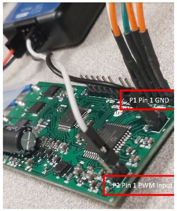
Step 3: Power supply to the PWM controller.
Connect the Switching regular input to the battery terminals and the output (5V) to the PWM controller supply.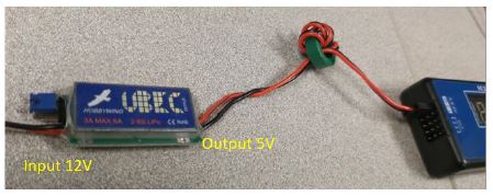
Step 4: PWM controller configuration:
The signal pulse width from the PWM controller is validated for a valid signal in firmware to prevent spurious turn ON and overspeeding. The controller has two push-button switches. Select the manual mode of operation using the “Select” switch. Use the “Pulse Width” button to select between 3 levels of speed control. The switch cycles through 3 ranges for PWM duty cycle output with each press.
- Range 1: 4-11%
- Range 2: 10-27.5%
- Range 3: 20-55%
The display indication varies from 800 to 2200 for a linear change in duty cycle within the range. Turning the potentiometer on the PWM controller will increase or decrease the PWM output.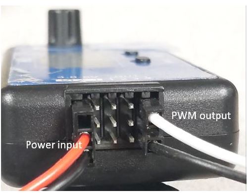
Step 5: Motor terminal connection:
Connect the motor terminals to PHASE A,B, and C. The sequence decides the direction of rotation of the motor. The desired rotation of the Drone is clockwise looking into the motor to prevent the propeller from loosening. It is therefore important to confirm the rotation direction before mounting the blades. Supply a PWM reference signal by tweaking the potentiometer on the PWM controller starting with the least pulse width position (800). The motor will start spinning at 7.87% duty cycle (50Hz) and above. The 7-Segment display shows 1573 (7.87% duty cycle) to 1931 (10.8% duty cycle) when the motor spins. Confirm the direction of rotation is counterclockwise. If not swap any two connections to the motor terminals. Return the potentiometer to the lowest speed setting.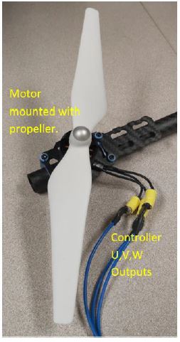
Step 6: Mounting the Propeller:
Disconnect battery power. Mount the propeller blade by screwing it into the motor shaft in a clockwise direction. Hold the stick/motor firmly with the arm stretched out and at a safe distance from all obstacles and people while in operation. Connect the power supply. The propeller action will exert force against the hand when spinning, so a firm grip is essential to prevent bodily injury. Tweak the potentiometer to change the speed (display indicates between 1573 and 1931) This completes the demonstration.
The below picture shows the overall wiring setup for the demonstration.

Schematics
BOARD SCHEMATICS
This section provides schematics diagrams of the dsPIC33EP32MC204 Drone Propeller Reference Design. The reference design uses a four-layer FR4, 1.6 mm, Plated-Through-Hole (PTH) construction.
Table A-1 summarizes the schematics of the Reference Design:
| TABLE A-1: SCHEMATICS | ||
| Figure Index | Schematics Sheet No. | Hardware Sections |
|
Figure A-1 |
1 of 4 |
dsPIC33EP32MC204-dsPIC DSC(U1) Interconnections MCP8026-MOSFET driver interconnections
3.3V analog and digital filter and feedback network dsPIC DSC internal operational amplifiers for amplifying Bus Current Bootstrap network. |
|
Figure A-2 |
2 of 4 |
In-System Serial Programming Header ISP1 CAN Communication Interface Header P5 External PWM speed control Interface Header P2
Serial Debugger Interface P3 |
|
Figure A-3 |
3 of 4 |
DC Bus voltage scaling resistor divider Back-emf voltage scaling network
Op-Amp gain and reference circuitry for phase current sensing |
| Figure A-4 | 4 of 4 | Motor Control Inverter –Three-phase MOSFET bridge |
Figure A-1:

Figure A-2

Figure A-4

Electrical Specifications
INTRODUCTION
This section provides the electrical specifications for the dsPIC33EP32MC204 Drone Motor Controller Reference Design (see Table B-1).
ELECTRICAL SPECIFICATIONS 1:
| Parameter | Operating Range |
| Input DC Voltage | 10-14V |
| Absolute Maximum Input DC Voltage | 20V |
| Maximum Input Current through Connector VDC and GND | 10A |
| Continuous Output Current per phase @ 25°C | 44A (Peak) |
| Motor Specifications: DJI 2312 | |
| Motor Phase Resistance | 42-47 milli Ohms |
| Motor Phase Inductance | 7.5 micro-Henrys |
| Motor Pole Pairs | 4 |
Note:
- While operating at an ambient temperature of +25°C and within the permissible Input DC voltage range the board remains within thermal limits for continuous per phase currents of up to 5A (RMS).
Bill of Materials (BOM)
BILL OF MATERIALS
| Item | Comment | Designator | Quantity |
| 1 | 10uF 25V 10% 1206 | C1 | 1 |
| 2 | 10uF 25V 10% 0805 | C2,C17, C18 | 3 |
| 3 | 1uF 25V 10% 0402 | C3, C5 | 2 |
| 4 | 22uF 25V 20% 0805 | C4 | 1 |
| 5 | 100nF 25V 0402 | C6 | 1 |
| 6 | 2.2uF 10V 0402 | C24, C26 | 2 |
| 7 | 1uF 25V 10% 0603 | C7, C8, C9, C10, C12, C13 | 6 |
| 8 | 100nF 50V 10% 0603 | C11, C14, C15, C20 | 4 |
| 9 | 1.8nF 50V 10% 0402 | C16 | 1 |
| 10 | 0.01uF 50V 10% 0603 | C19, C23, C27,C25 | 3 |
| 11 | 100pF 50V 5% 0603 | C21, C22 | 2 |
| 12 | 680uF 25V 10% RB2/4 | C28 | 1 |
| 13 | 5.6nF 50V 10% 0603 | C29, C30 | 2 |
| 14 | 1N5819 SOD323 | D1, D2, D3, D7 | 4 |
| 15 | 1N5819 SOD323 | D4, D5, D6 | 3 |
| 16 | 4.7uF 25V 10% 0805 | E1 | 1 |
| 17 | TPHR8504PL SOP8 | NMOS1, NMOS2, NMOS3, NMOS4, NMOS5, NMOS6 | 6 |
| 18 | 15uH 1A SMD4*4 | P4 | 1 |
| 19 | 200R 1% 0603 | R1, R2 | 2 |
| 20 | 0R 1% 0603 | R5,R27 | 2 |
| 21 | 47K 1% 0603 | R4, R6, R14, R24 | 4 |
| 22 | 47R 1% 0402 | R7, R8, R9, R18, R19, R20 | 6 |
| 23 | 2K 1% 0603 | R10, R37, R38, R39, R40, R42, R45, R46, R48, R49, R54, R57 | 12 |
| 24 | 300K 1% 0402 | R11, R12, R13 | 3 |
| 25 | 24.9R 1% 0603 | R15, R16, R17 | 3 |
| 26 | 100K 1% 0402 | R21, R22, R23 | 3 |
| 27 | 0.01R 1% 2010 | R25,R26 | 1 |
| 28 | 0R 1% 0805 | R28 | 1 |
| 29 | bead 1R 0603 | R29 | 1 |
| 30 | 18K 1% 0603 | R30 | 1 |
| 31 | 4.99R 1% 0603 | R31 | 1 |
| 32 | 11K 1% 0603 | R32 | 1 |
| 33 | 30K 1% 0603 | R33, R34, R47, R50 | 4 |
| 34 | 300R 1% 0603 | R35, R44, R55 | 3 |
| 35 | 20k 1% 0603 | R36 | 1 |
| 36 | 12K 1% 0603 | R41, R53, R56 | 3 |
| 37 | 10K 1% 0603 | R43, R52 | 2 |
| 38 | 1k 1% 0603 | R51 | 1 |
| 39 | 330R 1% 0603 | R58, R59 | 2 |
| 40 | DSPIC33EP64MC504-I/PT TQFP44 | U1 | 1 |
| 41 | MCP8026-48L TQFP48 | U2 | 1 |
| 42 | 2 PIN-68016-106HLF | P1, P2, P3 | 3 |
| 43 | 5 PIN-68016-106HLF | ISP1 | 1 |
| 44 | 6 PIN-68016-106HLF | P5 | 1 |
Test Results
Tests were performed to characterize the Drone Propeller Reference Design. A 12V, four pole pair three-phase PMSM Drone motor shown in the setup on page 1 was used for testing with blades attached. Table D-1 summarizes the test results. Figure D-1 shows the speed vs. input power.
Table D-1

Figure D-1

Documents / Resources
 |
MICROCHIP dsPIC33EP32MC204 Drone Propeller Reference Design [pdf] User Guide dsPIC33EP32MC204, dsPIC33EP32MC204 Drone Propeller Reference Design, Drone Propeller Reference Design, Propeller Reference Design, Reference Design, Design |
 |
MICROCHIP dsPIC33EP32MC204 Drone Propeller Reference Design [pdf] Instructions DS70005545A, DS70005545, 70005545A, 70005545, dsPIC33EP32MC204 Drone Propeller Reference Design, dsPIC33EP32MC204, Drone Propeller Reference Design, Propeller Reference Design, Reference Design, Design |


