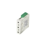
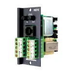
EMKO PROOP Input or Output Module

Preface
Proop-I/O Module is used with the Prop device. It can also be used as a data path for any brand. This document will be helpful the user to install and connect Proop-I/O Module.
- Before beginning the installation of this product, please read the instruction manual.
- The contents of the document may have been updated. You can access the most updated version at www.emkoelektronik.com.tr
- This symbol is used for safety warnings. User must pay attention to these warnings.
Environmental Conditions
| Operating Temperature : | 0-50C |
| Maximum Humidity : | 0-90 %RH (None Condensing) |
| Weight : | 238gr |
| Dimension : | 160 x 90 x 35 mm |
Features
Proop-I/O modules are divided into several types according to inputs-outputs. The types are as follows.
| Product Type
Proop-I/O.P. |
A |
. |
B |
. |
C |
. |
D |
. |
E |
. |
F |
| 2 | 2 | 1 | 3 | ||||||||
| Module Supply | |||||||||||
| 24 Vdc/Vac (Isolation) | 2 | |||
| Communication | ||||
| RS-485 (Isolation) | 2 | |||
| Digital Inputs | ||||
| 8x Digital | 1 | |||
| Digital Outputs | ||||
| 8x 1A Transistor (+V) | 3 | |||
| Analog Inputs | ||||
| 5x Pt-100 (-200…650°C)
5x 0/4..20mAdc 5x 0…10Vdc 5x 0…50mV |
1 | ||
| 2 | |||
| 3 | |||
| 4 | |||
| Analog Outputs | |||
| 2x 0/4…20mAdc
2x 0…10Vdc |
1 | ||
| 2 | |||
Dimensions
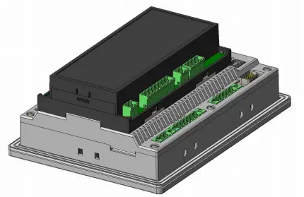
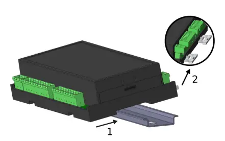
Mounting of Module on Proop Device
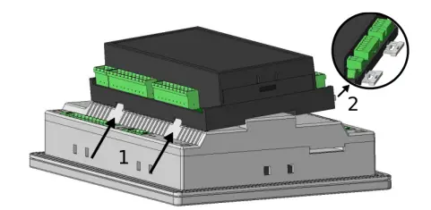 |
1- Insert the Prop I/O Module into the holes of the Prop device as in the picture.
2- Check the locking parts are plugged into the Proop-I/ O Module device and pulled out. |
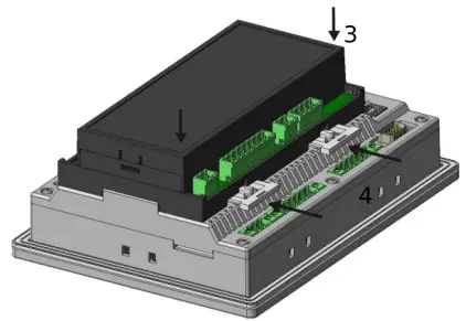 |
3- Press the Proop-I / O Module device firmly in the specified direction.
4- Insert the locking parts by pushing them in. |
 |
5- The inserted image of module device should look like the one on the left. |
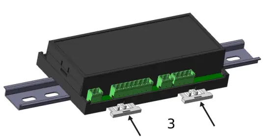
Mounting of Module on DIN-Ray
 |
1- Drag the Proop-I/O Module device onto the DIN-ray as shown.
2- Check the locking parts are plugged into the Prop- I/O Module device and pulled out. |
 |
3- Insert the locking parts by pushing them in. |
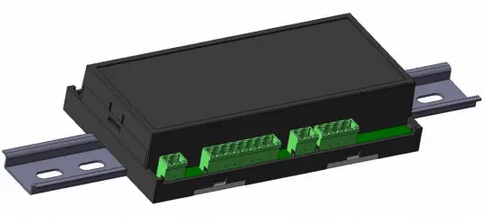 |
4- The inserted image of the module device should look like the one on the left. |
Installation
- Before beginning installation of this product, please read the instruction manual and warnings below carefully.
- A visual inspection of this product for possible damage occured during shipment is recommended before installation. It is your responsibility to ensure that qualified mechanical and electrical technicians install this product.
- Do not use the unit in combustible or explosive gaseous atmospheres.
- Do not expose the unit to direct sun rays or any other heat source.
- Do not place the unit in the neighbourhood of magnetic equipment such as transformers, motors or devices which generate interference (welding machines, etc.)
- To reduce the effect of electrical noise on device, Low voltage line (especially sensor input cable) wiring must be separated from high current and voltage line.
- During installation of the equipment in the panel, sharp edges on metal parts can cause cuts on the hands, please use caution.
- Mounting of the product must be done with its own mounting clamps.
- Do not mount the device with inappropriate clamps. Do not drop the device during installation.
- If possible, use shielded cable. To prevent ground loops the shield should be grounded on one end only.
- To prevent electric shock or damage to the device, do not apply power to the device until all of the wiring is completed.
- The digital outputs and supply connections are designed to be isolated from each other.
- Before commissioning the device, parameters must be set in accordance with desired use.
- Incomplete or incorrect configuration can be dangerous.
- The unit is normally supplied without a power switch, fuse, or circuit breaker. Use a power switch, fuse, and circuit breaker as required by local regulations.
- Apply only the rated power supply voltage to the unit, to prevent equipment damage.
- If there is danger of serious accident resulting from a failure or defect in this unit, power off the system and disconnect the device from the system.
- Never attempt to disassemble, modify or repair this unit. Tampering with the unit may result in malfunction, electric shock, or fire.
- Please contact us with any questions related to the safe operation of this unit.
- This equipment must be used in the manner specified in this instruction manual.
Connections
Power Supply
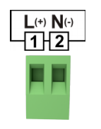 |
Terminal |
| + | |
|
– |
Communication Link with HMI Device
 |
Terminal |
| A | |
| B | |
| GND |
Digital Inputs
|
|
Terminal | Comment | Connection Sheme |
| DI8 |
Digital Inputs |
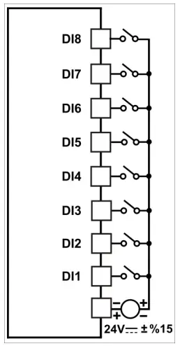 |
|
| DI7 | |||
| DI6 | |||
| DI5 | |||
| DI4 | |||
| DI3 | |||
| DI2 | |||
| DI1 | |||
|
+/- |
NPN / PNP
Selection of Digital Inputs |
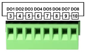
Digital Outputs
|
|
Terminal | Comment | Connection Scheme |
| DO1 |
Digital Outputs |
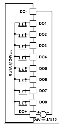 |
|
| DO2 | |||
| DO3 | |||
| DO4 | |||
| DO5 | |||
| DO6 | |||
| DO7 | |||
| DO8 |
Analog Inputs
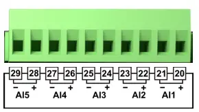
|
Terminal | Comment | Connection Scheme |
| AI5- |
Analog Input5 |
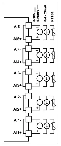 |
|
| AI5+ | |||
| AI4- |
Analog Input4 |
||
| AI4+ | |||
| AI3- |
Analog Input3 |
||
| AI3+ | |||
| AI2- |
Analog Input2 |
||
| AI2+ | |||
| AI1- |
Analog Input1 |
||
| AI1+ |
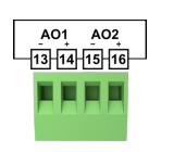
Analog Outputs
|
|
Terminal | Comment | Connection Scheme |
|
AO+ |
Analog Output Supply |
 |
|
|
AO- |
|||
|
AO1 |
Analog Outputs |
||
|
AO2 |
Technical Features
Power Supply
| Power Supply | : | 24VDC |
| Permissible Range | : | 20.4 – 27.6 VDC |
| Power Consumption | : | 3W |
Digital Inputs
| Digital Inputs | : | 8 Input | |
| Nominal Input Voltage | : | 24 VDC | |
|
Input Voltage |
: |
For Logic 0 | For Logic 1 |
| < 5 VDC | >10 VDC | ||
| Input Current | : | 6mA max. | |
| Input Impedance | : | 5.9 kΩ | |
| Response Time | : | ‘0’ to ‘1’ 50ms | |
| Galvanic Isolation | : | 500 VAC for 1 minute | |
High Speed Counter Inputs
| HSC Inputs | : | 2 Input(HSC1: DI1 and DI2, HSC2: DI3 and DI4) | |
| Nominal Input Voltage | : | 24 VDC | |
|
Input Voltage |
: |
For Logic 0 | For Logic 1 |
| < 10 VDC | >20 VDC | ||
| Input Current | : | 6mA max. | |
| Input Impedance | : | 5.6 kΩ | |
| Frequency range | : | 15KHz max. for single phase 10KHz max. for double phase | |
| Galvanic Isolation | : | 500 VAC for 1 minute | |
Digital Outputs
| Digital Outputs | 8 Output | |
| Outputs Current | : | 1 A max. (Total current 8 A max.) |
| Galvanic Isolation | : | 500 VAC for 1 minute |
| Short Circuit Protection | : | Yes |
Analog Inputs
| Analog Inputs | : | 5 Input | |||
|
Input Impedance |
: |
PT-100 | 0/4-20mA | 0-10V | 0-50mV |
| -200oC-650oC | 100Ω | >6.6kΩ | >10MΩ | ||
| Galvanic Isolation | : | No | |||
| Resolution | : | 14 Bits | |||
| Accuracy | : | ±0,25% | |||
| Sampling Time | : | 250 ms | |||
| Status Indication | : | Yes | |||
Analog Outputs
|
Analog Output |
: |
2 Output | |
| 0/4-20mA | 0-10V | ||
| Galvanic Isolation | : | No | |
| Resolution | : | 12 Bits | |
| Accuracy | : | 1% of full scale | |
Internal Address Definitions
Communication Settings:
| Parameters | Address | Options | Default |
| ID | 40001 | 1–255 | 1 |
| BAUDRATE | 40002 | 0- 1200 / 1- 2400 / 2- 4000 / 3- 9600 / 4- 19200 / 5- 38400 /
6- 57600 /7- 115200 |
6 |
| STOP BIT | 40003 | 0- 1Bit / 1- 2Bit | 0 |
| PARITY | 40004 | 0- None / 1- Even / 2- Odd | 0 |
Device addresses:
| Memory | Format | Arange | Address | Type |
| Digital Input | DIn | n: 0 – 7 | 10001 – 10008 | Read |
| Digital Output | DOn | n: 0 – 7 | 1 – 8 | Read-Write |
| Analog Input | AIn | n: 0 – 7 | 30004 – 30008 | Read |
| Analog Output | AOn | n: 0 – 1 | 40010 – 40011 | Read-Write |
| Version* | (aaabbbbbcccccccc)bit | n: 0 | 30001 | Read |
- Note:The a bits in this address are major, b bits are minor version number, c bits indicate device type.
- Example: Value read from 30001 (0x2121)hex = (0010000100100001)bit ,
- a bits (001)bit = 1 (Major version number)
- b bits (00001)bit = 1 (Minor version number)
- c bits (00100001)bit = 33 (The device types are indicated in the table.) Device version = V1.1
- Device type = 0-10V Analog Input 0-10V Analog Output
Device Types:
| Device Type | Value |
| PT100 Analog Input 4-20mA Analog Output | 0 |
| PT100 Analog Input 0-10V Analog Output | 1 |
| 4-20mA Analog Input 4-20mA Analog Output | 16 |
| 4-20mA Analog Input 0-10V Analog Output | 17 |
| 0-10V Analog Input 4-20mA Analog Output | 32 |
| 0-10V Analog Input 0-10V Analog Output | 33 |
| 0-50mV Analog Input 4-20mA Analog Output | 48 |
| 0-50mV Analog Input 0-10V Analog Output | 49 |
The conversion of the values read from the module according to the analog input type is described in the following table:
| Analog Input | The Value Range | Conversion Factor | Example of value shown in PROOP |
|
PT-100 -200° – 650° |
-2000 – 6500 |
x10–1 |
Example-1: The read value as 100 is converted to 10oC. |
| Example-2: The read value as 203 is converted to 20.3oC. | |||
| 0 – 10V | 0 – 20000 | 0.5×10⁻³ | Example-1: The read value as 2500 is converted to 1.25V. |
| 0 – 50mV | 0 – 20000 | 2.5×10⁻³ | Example-1: The read value as 3000 is converted to 7.25mV. |
|
0/4 – 20mA |
0 – 20000 |
0.1×10⁻³ |
Example-1: The read value as 3500 is converted to 7mA. |
| Example-2: The read value as 1000 is converted to 1mA. |
The conversion of the values write at the module according to the analog output type is described in the following table:
| Analog Output | The Value Range | Conversion Rate | Example of Value Written in Modules |
| 0 – 10V | 0 – 10000 | x103 | Example-1: The value to be written as 1.25V is converted to 1250. |
| 0/4 – 20mA | 0 – 20000 | x103 | Example-1: The value to be written as 1.25mA is converted to 1250. |
Analog Input-Specific Addresses:
| Parameter | AI1 | AI2 | AI3 | AI4 | AI5 | Default |
| Configuration Bits | 40123 | 40133 | 40143 | 40153 | 40163 | 0 |
| Minimum Scale Value | 40124 | 40134 | 40144 | 40154 | 40164 | 0 |
| Maximum Scale Value | 40125 | 40135 | 40145 | 40155 | 40165 | 0 |
| Scaled Value | 30064 | 30070 | 30076 | 30082 | 30088 | – |
Analog Input Configuration Bits:
| AI1 | AI2 | AI3 | AI4 | AI5 | Description |
| 40123.0bit | 40133.0bit | 40143.0bit | 40153.0bit | 40163.0bit | 4-20mA/2-10V Select:
0 = 0-20 mA/0-10 V 1 = 4-20 mA/2-10 V |
The Scaled Value for analog inputs is calculated according to the state of the 4-20mA / 2-10V Selection configuration bit.
Analog Output Specific Addresses:
| Parameter | AO1 | AO2 | Default |
| Minimum Scale Value for Input | 40173 | 40183 | 0 |
| Maximum Scale Value for Input | 40174 | 40184 | 20000 |
| Minimum Scale Value for Output | 40175 | 40185 | 0 |
| Maximum Scale Value for Output | 40176 | 40186 | 10000/20000 |
| Analog Output Function
0: Manual use 1: Using the scale values above, it reflects the input to the output. 2: It drives the analog output as PID output, using the minimum and maximum scale parameters for the output. |
40177 | 40187 | 0 |
- In case the analog output function parameter is set to 1 or 2;
- AI1 is used as input for A01 output.
- AI2 is used as input for A02 output.
- Not: Mirroring the input to output feature (Analoque Output Function = 1) cannot be used in modules with PT100 inputs.
HSC(High-Speed Counter) Settings
Single Phase Counter Connection
- High-speed counters count high-speed events that cannot be controlled at PROOP-IO scan rates. The maximum counting frequency of a high-speed counter is 10kHz for Encoder inputs and 15kHz for counter inputs.
- There are five basic types of counters: single-phase counter with internal direction control, single-phase counter with external direction control, two-phase counter with 2 clock inputs, A/B phase quadrature counter, and frequency measurement type.
- Note that every mode is not supported by every counter. You can use each type except the frequency measurement type: without reset or start inputs, with reset and without start, or with both start and reset inputs.
- When you activate the reset input, it clears the current value and holds it clear until you deactivate reset.
- When you activate the start input, it allows the counter to count. While start is deactivated, the current value of the counter is held constant and clocking events are ignored.
- If reset is activated while start is inactive, the reset is ignored and the current value is not changed. If the start input becomes active while the reset input is active, the current value is cleared.
| Parameters | Address | Default |
| HSC1 Configuration ve Mode Select* | 40012 | 0 |
| HSC2 Configuration ve Mode Select* | 40013 | 0 |
| HSC1 New Current Value (Least Significant 16 byte) | 40014 | 0 |
| HSC1 New Current Value (Most Significant 16 byte) | 40015 | 0 |
| HSC2 New Current Value (Least Significant 16 byte) | 40016 | 0 |
| HSC2 New Current Value (Most Significant 16 byte) | 40017 | 0 |
| HSC1 Current Value (Least Significant 16 byte) | 30010 | 0 |
| HSC1 Current Value (Most Significant 16 byte) | 30011 | 0 |
| HSC2 Current Value (Least Significant 16 byte) | 30012 | 0 |
| HSC2 Current Value (Most Significant 16 byte) | 30013 | 0 |
Note: This parameter;
- The least significant byte is the Mode parameter.
- The most significant byte is the Configuration parameter.
HSC Configuration Description:
| HSC1 | HSC2 | Description |
| 40012.8bit | 40013.8bit | Active level control bit for Reset:
0 = Reset is active low 1 = Reset is active high |
| 40012.9bit | 40013.9bit | Active level control bit for Start:
0 = Start is active low 1 = Start is active high |
| 40012.10bit | 40013.10bit | Counting direction control bit:
0 = Count down 1 = Count up |
| 40012.11bit | 40013.11bit | Write the new current value to the HSC:
0 = No update 1 = Update current value |
| 40012.12bit | 40013.12bit | Enable the HSC:
0 = Disable the HSC 1 = Enable the HSC |
| 40012.13bit | 40013.13bit | Reserve |
| 40012.14bit | 40013.14bit | Reserve |
| 40012.15bit | 40013.15bit | Reserve |
HSC Modes:
| Mode | Description | Inputs | |||
| HSC1 | DI1 | DI2 | DI5 | DI6 | |
| HSC2 | DI3 | DI4 | DI7 | DI8 | |
| 0 | Single Phase Counter with Internal Direction | Clock | |||
| 1 | Clock | Reset | |||
| 2 | Clock | Reset | Start | ||
| 3 | Single Phase Counter with External Direction | Clock | Direction | ||
| 4 | Clock | Direction | Reset | ||
| 5 | Clock | Direction | Reset | Start | |
| 6 | Two Phase Counter with 2 Clock Input | Clock Up | Clock Down | ||
| 7 | Clock Up | Clock Down | Reset | ||
| 8 | Clock Up | Clock Down | Reset | Start | |
| 9 | A/B Phase Encoder Counter | Clock A | Clock B | ||
| 10 | Clock A | Clock B | Reset | ||
| 11 | Clock A | Clock B | Reset | Start | |
| 12 | Reserve | ||||
| 13 | Reserve | ||||
| 14 | Period Measurement (with 10 μs sampling time) | Period Input | |||
| 15 | Counter /
Period Ölçümü (1ms sampling time) |
Max. 15 kHz | Max. 15 kHz | Max. 1 kHz | Max. 1 kHz |
Specific Addresses for Mode 15:
| Parameter | DI1 | DI2 | DI3 | DI4 | DI5 | DI6 | DI7 | DI8 | Default |
| Configuration Bits | 40193 | 40201 | 40209 | 40217 | 40225 | 40233 | 40241 | 40249 | 2 |
| Period Reset Time (1-1000 sn) |
40196 |
40204 |
40212 |
40220 |
40228 |
40236 |
40244 |
40252 |
60 |
| Counter low-order 16-bit value | 30094 | 30102 | 30110 | 30118 | 30126 | 30134 | 30142 | 30150 | – |
| Counter high-order 16-bit value | 30095 | 30103 | 30111 | 30119 | 30127 | 30135 | 30143 | 30151 | – |
| Period low-order 16-bit value(ms) | 30096 | 30104 | 30112 | 30120 | 30128 | 30136 | 30144 | 30152 | – |
| Period high-order 16-bit value(ms) | 30097 | 30105 | 30113 | 30121 | 30129 | 30137 | 30145 | 30153 | – |
Configuration Bits:
| DI1 | DI2 | DI3 | DI4 | DI5 | DI6 | DI7 | DI8 | Description |
| 40193.0bit | 40201.0bit | 40209.0bit | 40217.0bit | 40225.0bit | 40233.0bit | 40241.0bit | 40249.0bit | DIx enable bit: 0 = DIx enable 1 = DIx disable |
|
40193.1bit |
40201.1bit |
40209.1bit |
40217.1bit |
40225.1bit |
40233.1bit |
40241.1bit |
40249.1bit |
Count direction bit:
0 = Count down 1 = Count up |
| 40193.2bit | 40201.2bit | 40209.2bit | 40217.2bit | 40225.2bit | 40233.2bit | 40241.2bit | 40249.2bit | Reserve |
| 40193.3bit | 40201.3bit | 40209.3bit | 40217.3bit | 40225.3bit | 40233.3bit | 40241.3bit | 40249.3bit | DIx count reset bit:
1 = Reset the DIx counter |
PID Settings
The PID or On/Off control feature can be used by setting the parameters determined for each analog input in the module. The analog input with PID or ON/OFF function activated controls the corresponding digital output. The digital output associated with the channel whose PID or ON/OFF function is activated cannot be driven manually.
- Analog input AI1 controls digital output DO1.
- Analog input AI2 controls digital output DO2.
- Analog input AI3 controls digital output DO3.
- Analog input AI4 controls digital output DO4.
- Analog input AI5 controls digital output DO5.
PID Parameters:
| Parameter | Description |
| PID Active | Enables PID or ON/OFF operation.
0 = Manual use 1 = PID active 2 = ON/OFF active |
| Set Value | It is the set value for PID or ON/OFF operation. PT100 values can be between -200.0 and 650.0 for input, 0 and 20000 for other types. |
| Set Offset | It is used as Set Offset value in PID operation. It can take values between -325.0 and
325.0 for PT100 input, -10000 to 10000 for other types. |
| Set Hysteresis | It is used as Set Hysteresis value in ON/OFF operation. It can take values between
-325.0 and 325.0 for PT100 input, -10000 to 10000 for other types. |
| Minimum Scale Value | Working scale is the lower limit value. PT100 values can be between -200.0 and
650.0 for input, 0 and 20000 for other types. |
| Maximum Scale Value | Working scale is the upper limit value. PT100 values can be between -200.0 and
650.0 for input, 0 and 20000 for other types. |
| Heating Proportional Value | Proportional value for heating. It can take values between 0.0 and 100.0. |
| Heating Integral Value | Integral value for heating. It can take values between 0 and 3600 seconds. |
| Heating Derivative Value | Derivative value for heating. It can take values between 0.0 and 999.9. |
| Cooling Proportional Value | Proportional value for cooling. It can take values between 0.0 and 100.0. |
| Cooling Integral Value | Integral value for cooling. It can take values between 0 and 3600 seconds. |
| Cooling Derivative Value | Derivative value for cooling. It can take values between 0.0 and 999.9. |
| Output Period | Output is the control period. It can take values between 1 and 150 seconds. |
| Heating/Cooling Select | Specifies the channel operation for PID or ON/OFF. 0 = Heating 1 = Cooling |
| Auto Tune | Starts Auto Tune operation for PID.
0 = Auto Tune passive 1 = Auto Tune active |
- Note: For the values in dotted notation, 10 times the real value of these parameters are used in Modbus communication.
PID Modbus Addresses:
| Parameter | AI1
Address |
AI2
Address |
AI3
Address |
AI4
Address |
AI5
Address |
Default |
| PID Active | 40023 | 40043 | 40063 | 40083 | 40103 | 0 |
| Set Value | 40024 | 40044 | 40064 | 40084 | 40104 | 0 |
| Set Offset | 40025 | 40045 | 40065 | 40085 | 40105 | 0 |
| Sensor Offset | 40038 | 40058 | 40078 | 40098 | 40118 | 0 |
| Set Hysteresis | 40026 | 40046 | 40066 | 40086 | 40106 | 0 |
| Minimum Scale Value | 40027 | 40047 | 40067 | 40087 | 40107 | 0/-200.0 |
| Maximum Scale Value | 40028 | 40048 | 40068 | 40088 | 40108 | 20000/650.0 |
| Heating Proportional Value | 40029 | 40049 | 40069 | 40089 | 40109 | 10.0 |
| Heating Integral Value | 40030 | 40050 | 40070 | 40090 | 40110 | 100 |
| Heating Derivative Value | 40031 | 40051 | 40071 | 40091 | 40111 | 25.0 |
| Cooling Proportional Value | 40032 | 40052 | 40072 | 40092 | 40112 | 10.0 |
| Cooling Integral Value | 40033 | 40053 | 40073 | 40093 | 40113 | 100 |
| Cooling Derivative Value | 40034 | 40054 | 40074 | 40094 | 40114 | 25.0 |
| Output Period | 40035 | 40055 | 40075 | 40095 | 40115 | 1 |
| Heating/Cooling Select | 40036 | 40056 | 40076 | 40096 | 40116 | 0 |
| Auto Tune | 40037 | 40057 | 40077 | 40097 | 40117 | 0 |
| PID Instant Output Value (%) | 30024 | 30032 | 30040 | 30048 | 30056 | – |
| PID Status Bits | 30025 | 30033 | 30041 | 30049 | 30057 | – |
| PID Configuration Bits | 40039 | 40059 | 40079 | 40099 | 40119 | 0 |
| Auto Tune Status Bits | 30026 | 30034 | 30042 | 30050 | 30058 | – |
PID Configuration Bits :
| AI1 Address | AI2 Address | AI3 Address | AI4 Address | AI5 Address | Description |
| 40039.0bit | 40059.0bit | 40079.0bit | 40099.0bit | 40119.0bit | PID pause:
0 = PID operation continues. 1 = PID is stopped and the output is turned off. |
PID Status Bits :
| AI1 Address | AI2 Address | AI3 Address | AI4 Address | AI5 Address | Description |
| 30025.0bit | 30033.0bit | 30041.0bit | 30049.0bit | 30057.0bit | PID calculation status:
0 = Calculating PID 1 = PID is not calculated. |
|
30025.1bit |
30033.1bit |
30041.1bit |
30049.1bit |
30057.1bit |
Integral calculation status:
0 = Calculating integral 1 = Integral is not calculated |
Auto-Tune Status Bits :
| AI1 Address | AI2 Address | AI3 Address | AI4 Address | AI5 Address | Description |
| 30026.0bit | 30034.0bit | 30042.0bit | 30050.0bit | 30058.0bit | Auto Tune first step status:
1 = The first step is active. |
| 30026.1bit | 30034.1bit | 30042.1bit | 30050.1bit | 30058.1bit | Auto Tune second step status:
1 = The second step is active. |
| 30026.2bit | 30034.2bit | 30042.2bit | 30050.2bit | 30058.2bit | Auto Tune third step status:
1 = The third step is active. |
| 30026.3bit | 30034.3bit | 30042.3bit | 30050.3bit | 30058.3bit | Auto Tune final step status:
1 = Auto Tune complete. |
| 30026.4bit | 30034.4bit | 30042.4bit | 30050.4bit | 30058.4bit | Auto Tune Timeout error:
1 = There is a timeout. |
Installing Communication Settings by Default
For cards with version V01;
- Power off the I/O Module device.
- Lift the cover of the device.
- Short circuit pins 2 and 4 on the socket shown in the picture.
- Wait for at least 2 seconds by energizing. After 2 seconds, the communication settings will return to default.
- Remove the short circuit.
- Close the device cover.
For cards with version V02;
- Power off the I/O Module device.
- Lift the cover of the device.
- Put a jumper on the socket shown in the picture.
- Wait for at least 2 seconds by energizing. After 2 seconds, the communication settings will return to default.
- Remove the jumper.
- Close the device cover.
Modbus Slave Address Selection
The slave address can be set from 1 to 255 at address 40001 of the modbus. In addition, the Dip Switch on the card can be used to set the slave address on V02 cards.
| DIP SWITCH | ||||
| SLAVE ID | 1 | 2 | 3 | 4 |
| Not1 | ON | ON | ON | ON |
| 1 | OFF | ON | ON | ON |
| 2 | ON | OFF | ON | ON |
| 3 | OFF | OFF | ON | ON |
| 4 | ON | ON | OFF | ON |
| 5 | OFF | ON | OFF | ON |
| 6 | ON | OFF | OFF | ON |
| 7 | OFF | OFF | OFF | ON |
| 8 | ON | ON | ON | OFF |
| 9 | OFF | ON | ON | OFF |
| 10 | ON | OFF | ON | OFF |
| 11 | OFF | OFF | ON | OFF |
| 12 | ON | ON | OFF | OFF |
| 13 | OFF | ON | OFF | OFF |
| 14 | ON | OFF | OFF | OFF |
| 15 | OFF | OFF | OFF | OFF |
- Note 1: When all of the Dip Switches are ON, the value in Modbus register 40001 is used as the slave address.
Warranty
This product is warranted against defects in materials and workmanship for a period of two years from the date of shipment to Buyer. The Warranty is limited to repair or replacement of the defective unit at theoption of the manufacturer. This warranty is void if the product has been altered, misused, dismantled, or otherwise abused.
Maintenance
Repairs should only be performed by trained and specialized personnel. Cut power to the device before accessing internal parts. Do not clean the case with hydrocarbon-based solvents (Petrol, Trichlorethylene, etc.). Use of these solvents can reduce the mechanical reliability of the device.
Other Information
- Manufacturer Information:
- Emko Elektronik Sanayi ve Ticaret A.Ş.
- Bursa Organize Sanayi Bölgesi, (Fethiye OSB Mah.)
- Ali Osman Sönmez Bulvarı, 2. Sokak, No:3 16215
- BURSA/TURKEY
- Phone : (224) 261 1900
- Fax : (224) 261 1912
- Repair and maintenance service information:
- Emko Elektronik Sanayi ve Ticaret A.Ş.
- Bursa Organize Sanayi Bölgesi, (Fethiye OSB Mah.)
- Ali Osman Sönmez Bulvarı, 2. Sokak, No:3 16215
- BURSA/TURKEY
- Phone : (224) 261 1900
- Fax : (224) 261 1912
Documents / Resources
 |
EMKO PROOP Input or Output Module [pdf] User Manual PROOP, Input or Output Module, PROOP Input or Output Module, Input Module, Output Module, Module |