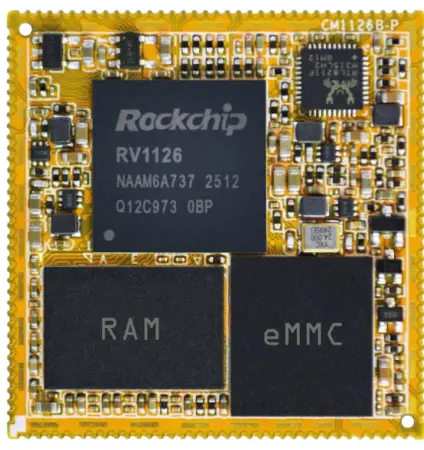
Boardcon Embedded CM1126B-P System on Module
fepetra arahana
| endri-javatra | fepetra arahana |
| Unité centrale | Quad-core Cortex-A53 |
| DDR | 2GB LPDDR4 (hatramin'ny 4GB) |
| eMMC FLASH | 8GB (hatramin'ny 256GB) |
| fahefana | DC 3.3V |
| MIPI DSI | 4-Lalana |
| I2S | 4-CH |
| MIPI CSI | 2-CH 4-Lalana |
| RGB LCD | 24 bit |
| Camera | 1-CH(DVP) sy 2-CH(CSI) |
| USB | 2-CH (USB HOST 2.0 and OTG 2.0) |
| Ethernet | 1000M GMAC |
| SDMMC | 2-CH |
| I2C | 5-CH |
| SPI | 2-CH |
| UART | 5-CH, 1-CH(DEBUG) |
| PWM | 11-CH |
| ADC IN | 4-CH |
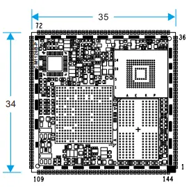
| Dimension board | 34 x 35 mm |
Sava lalana
Momba ity boky torolalana ity
Ity boky torolalana ity dia natao hanomezana ny mpampiasa mihoatraview of the board and its benefits, complete feature specifications, and setup procedures. It contains important safety information as well.
Hevitra sy Fanavaozana an'ity boky torolalana ity
Mba hanampiana ny mpanjifanay hanararaotra ny vokatray, dia tsy mitsahatra manome loharano fanampiny sy havaozina izahay ao amin'ny Boardcon webtranokala (www.boardcon.com, www.armdesigner.com). Anisan'izany ny boky fampianarana, naoty fampiharana, fandaharana examples, ary rindrambaiko sy fitaovana nohavaozina. Midira tsindraindray hahitana izay vaovao! Rehefa manao laharam-pahamehana ny asa amin'ireo loharano nohavaozina ireo izahay, ny valin-kafatra avy amin'ny mpanjifa no fiantraikany voalohany, Raha manana fanontaniana, fanehoan-kevitra, na ahiahy momba ny vokatrao na tetikasanao ianao dia aza misalasala mifandray aminay amin'ny support@armdesigner.com.
CM1126B-P Introduction
FAMINTINANA
The CM1126B-P system-on-module is equipped with Rockchip’s RV1126B-P, built with a quad-core Cortex-A53, 3.0 TOPs NPU, and RISC-V MCU. It is designed specifically for the IPC/CVR devices, AI Camera devices, intelligent interactive devices, and mini robots. High-performance and low-power solutions can help customers introduce new technologies more quickly and enhance the overall solution efficiency. The smallest size can be put on a 38board. Following the hardware revision from CM1126 (V1) to CM1126B-P (V2), where the SoC is updated to the RV1126B-P, the Reset & OTG_VBUS signals and the WIFI/BT module’s GPIO voltage must operate at a 3.3V logic level.
Toetoetra
Microprocessor
- Quad-core Cortex-A53 hatramin'ny 1.6GHz
- 32KB I-cache sy 32KB D-cache ho an'ny core tsirairay, 512KB L3 cache
- 3.0 TOPS Fizotry ny Neural Unit
- RISC-V MCU to support 250ms fast boot
- Max 12M ISP
Fandaminana fahatsiarovana
- LPDDR4 RAM hatramin'ny 4GB
- eMMC hatramin'ny 256GB
- SPI Flash hatramin'ny 8MB
Video Decoder/Encoder
- Manohana ny decode/encode video hatramin'ny 4K@30fps
- Manohana decoding amin'ny fotoana tena izy ny H.264/265
- Manohana famandrihana horonan-tsary UHD H.264/265 tena izy
- Haben'ny sary hatramin'ny 8192 × 8192
Asehoy ny Subsystem
- Video Output
- Manohana lalana 4 MIPI DSI hatramin'ny 2560×1440@60fps
- Supports 24-bit RGB parallel output
- Sary in
- Supports up to 16-bit DVP interface
- Manohana interface tsara 2ch MIPI CSI 4lanes
I2S/PCM/AC97
- Telo I2S/PCM interface tsara
- Tohano ny MIC array hatramin'ny 8ch PDM/TDM interface
- Manohana ny famoahana feo PWM
USB sy PCIE
- Roa 2.0 USB interface tsara
- One USB 2.0 OTG and one 2.0 USB host
Ethernet
- Takelaka data RTL8211F
- Fanohanana 10/100/1000M
I2C
- Hatramin'ny dimy I2C
- Tohano ny maody mahazatra sy ny fomba haingana (hatramin'ny 400kbit/s)
SDIO
- Tohano ny protocol 2CH SDIO 3.0
SPI
- Hatramin'ny roa SPI controllers,
- Full-duplex synchronous serial interface tsara
UART
- Manohana hatramin'ny 6 UARTs
- UART2 misy tariby 2 ho an'ny fitaovana debug
- Embedded two 664-byte FIFOs
- Tohano ny fomba fanaraha-maso ny fikorianan'ny fiara ho an'ny UART0/1/3/4/5
ADC
- Hatramin'ny fantsona ADC efatra
- 12-bit resolution
- BOKYtage ny fidirana eo anelanelan'ny 0V ka hatramin'ny 1.8V
- Manohana hatramin'ny 1MS/ssampling rate
PWM
- 11 on-chip PWM miaraka amin'ny fiasa mifototra amin'ny interrupt
- Support 32-bit time/counter facility
- Safidy IR amin'ny PWM3/7
Vondrona herinaratra
- Hery mitokana eny ambony sambo
- Fampidirana tokana 3.3V
CM1126B-P Block Diagram
RV1126B-P Block Diagram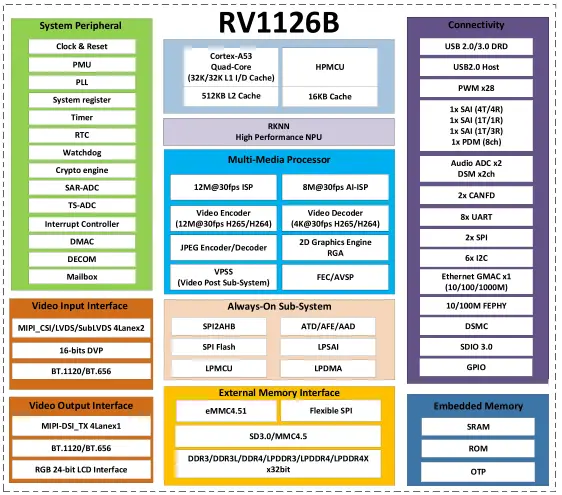
Birao fampandrosoana (Idea1126) Block Diagram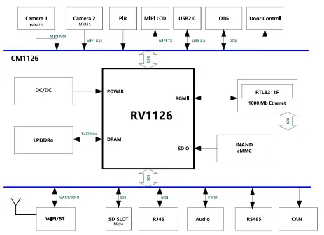
CM1126B-P PCB Dimension
CM1126B-P Pin Definition
| Pin | famantarana | Famaritana na fiasa | Serial GPIO | IO Voltage |
| 1 | LCDC_D19_3V3 | I2S1_MCLK_M2/CIF_D15_M1 | GPIO2_C7_d | 3.3V |
| 2 | LCDC_D20_3V3 | I2S1_SDO_M2/CIF_VS_M1 | GPIO2_D0_d | 3.3V |
| 3 | LCDC_D21_3V3 | I2S1_SCLK_M2/CIF_CLKO_M1 | GPIO2_D1_d | 3.3V |
| 4 | LCDC_D22_3V3 | I2S1_LRCK_M2/CIF_CKIN_M1 | GPIO2_D2_d | 3.3V |
| 5 | LCDC_D23_3V3 | I2S1_SDI_M2/CIF_HS_M1 | GPIO2_D3_d | 3.3V |
| 6 | GND | tany | 0V | |
| 7 | GPIO1_D1 | UART1_RX_M1/I2C5_SDA_M2 | GPIO1_D1_d | 3.3V(V2) |
| 8 | BT_WAKE | SPI0_CS1n_M0 | GPIO0_A4_u | 3.3V(V2) |
| 9 | WIFI_REG_ON | SPI0_MOSI_M0 | GPIO0_A6_d | 3.3V(V2) |
| 10 | BT_RST | SPI0_MISO_M0 | GPIO0_A7_d | 3.3V(V2) |
| 11 | WIFI_WAKE_HOST | SPI0_CLK_M0 | GPIO0_B0_d | 3.3V(V2) |
| 12 | BT_WAKE_HOST | SPI0_CS0n_M0 | GPIO0_A5_u | 3.3V(V2) |
| 13 | PWM7_IR_M0_3V3 | GPIO0_B1_d | 3.3V | |
| 14 | PWM6_M0_3V3 | TSADC_SHUT_M1 | GPIO0_B2_d | 3.3V |
| 15 | UART2_TX_3V3 | Ho an'ny debug | GPIO3_A2_u | 3.3V |
| 16 | UART2_RX_3V3 | Ho an'ny debug | GPIO3_A3_u | 3.3V |
| 17 | I2S0_MCLK_M0_3V
3 |
GPIO3_D2_d | 3.3V | |
| 18 | I2S0_SCLK_TX_M0
_3V3 |
ACODEC_DAC_CLK | GPIO3_D0_d | 3.3V |
| 19 | I2S0_SDI3_M0_3V3 | PDM_SDI3_M0 /
ACODEC_ADC_DATA |
GPIO3_D7_d | 3.3V |
| 20 | I2S0_SDO0_M0_3V
3 |
ACODEC_DAC_DATAR
/APWM_R_M1/ADSM_LP |
GPIO3_D5_d | 3.3V |
| Pin | famantarana | Famaritana na fiasa | Serial GPIO | IO Voltage |
| 21 | I2S0_LRCK_TX_M0
_3V3 |
ACODEC_DAC_SYNC
/APWM_L_M1/ADSM_LN |
GPIO3_D3_d | 3.3V |
| 22 | PDM_SDI1_3V3 | I2S0_SDO3_SDI1_M0/I2C4SDA | GPIO4_A1_d | 3.3V |
| 23 | PDM_CLK1_3V3 | I2S0_SCK_RX_M0 | GPIO3_D1_d | 3.3V |
| 24 | PDM_SDI2_3V3 | I2S0_SDO2_SDI2_M0/I2C4SCL | GPIO4_A0_d | 3.3V |
| 25 | PDM_SDI0_3V3 | I2S0_SDI0_M0 | GPIO3_D6_d | 3.3V |
| 26 | PDM_CLK_3V3 | I2S0_LRCK_RX_M0 | GPIO3_D4_d | 3.3V |
| 27 | I2C2_SDA_3V3 | PWM5_M0 | GPIO0_C3_d | 3.3V |
| 28 | I2C2_SCL_3V3 | PWM4_M0 | GPIO0_C2_d | 3.3V |
| 29 | USB_HOST_DP | 1.8V | ||
| 30 | USB_HOST_DM | 1.8V | ||
| 31 | GND | tany | 0V | |
| 32 | OTG_DP | Can be used for download | 1.8V | |
| 33 | OTG_DM | Can be used for download | 1.8V | |
| 34 | OTG_DET(V2) | OTG VBUS DET IN | 3.3V(V2) | |
| 35 | OTG_ID | 1.8V | ||
| 36 | SPI0_CS1n_M1 | I2S1_MCK_M1/UART4_TX_M2 | GPIO1_D5_d | 1.8V |
| 37 | VCC3V3_SYS | 3.3V Main Power fampidirana | 3.3V | |
| 38 | VCC3V3_SYS | 3.3V Main Power fampidirana | 3.3V | |
| 39 | USB_CTRL_3V3 | GPIO0_C1_d | 3.3V | |
| 40 | SDMMC0_DET | Tsy maintsy ampiasaina amin'ny karatra SD | GPIO0_A3_u | 3.3V(V2) |
| 41 | CLKO_32K | RTC famantaranandro Output | GPIO0_A2_u | 3.3V(V2) |
| 42 | nRESET | Avereno ny fampidirana fanalahidy | 3.3V(V2) | |
| 43 | MIPI_CSI_RX0_CL
KP |
MIPI CSI0 na LVDS0 fampidirana | 1.8V | |
| 44 | MIPI_CSI_RX0_CL
KN |
MIPI CSI0 na LVDS0 fampidirana | 1.8V | |
| 45 | MIPI_CSI_RX0_D2
P |
MIPI CSI0 na LVDS0 fampidirana | 1.8V | |
| 46 | MIPI_CSI_RX0_D2
N |
MIPI CSI0 na LVDS0 fampidirana | 1.8V | |
| 47 | MIPI_CSI_RX0_D3
P |
MIPI CSI0 na LVDS0 fampidirana | 1.8V | |
| 48 | MIPI_CSI_RX0_D3
N |
MIPI CSI0 na LVDS0 fampidirana | 1.8V | |
| 49 | MIPI_CSI_RX0_D1
P |
MIPI CSI0 na LVDS0 fampidirana | 1.8V | |
| 50 | MIPI_CSI_RX0_D1
N |
MIPI CSI0 na LVDS0 fampidirana | 1.8V | |
| 51 | MIPI_CSI_RX0_D0
P |
MIPI CSI0 na LVDS0 fampidirana | 1.8V |
| Pin | famantarana | Famaritana na fiasa | Serial GPIO | IO Voltage |
| 52 | MIPI_CSI_RX0_D0
N |
MIPI CSI0 na LVDS0 fampidirana | 1.8V | |
| 53 | GND | tany | 0V | |
| 54 | MIPI_CSI_RX1_D3
P |
MIPI CSI1 na LVDS1 fampidirana | 1.8V | |
| 55 | MIPI_CSI_RX1_D3
N |
MIPI CSI1 na LVDS1 fampidirana | 1.8V | |
| 56 | MIPI_CSI_RX1_CL
KP |
MIPI CSI1 na LVDS1 fampidirana | 1.8V | |
| 57 | MIPI_CSI_RX1_CL
KN |
MIPI CSI1 na LVDS1 fampidirana | 1.8V | |
| 58 | MIPI_CSI_RX1_D2
P |
MIPI CSI1 na LVDS1 fampidirana | 1.8V | |
| 59 | MIPI_CSI_RX1_D2
N |
MIPI CSI1 na LVDS1 fampidirana | 1.8V | |
| 60 | MIPI_CSI_RX1_D1
P |
MIPI CSI1 na LVDS1 fampidirana | 1.8V | |
| 61 | MIPI_CSI_RX1_D1
N |
MIPI CSI1 na LVDS1 fampidirana | 1.8V | |
| 62 | MIPI_CSI_RX1_D0
P |
MIPI CSI1 na LVDS1 fampidirana | 1.8V | |
| 63 | MIPI_CSI_RX1_D0
N |
MIPI CSI1 na LVDS1 fampidirana | 1.8V | |
| 64 | SDMMC0_D3_3V3 | UART3_TX_M1 | GPIO1_A7_u | 3.3V |
| 65 | SDMMC0_D2_3V3 | UART3_RX_M1 | GPIO1_A6_u | 3.3V |
| 66 | SDMMC0_D1_3V3 | UART2_TX_M0 | GPIO1_A5_u | 3.3V |
| 67 | SDMMC0_D0_3V3 | UART2_RX_M0 | GPIO1_A4_u | 3.3V |
| 68 | SDMMC0_CMD_3V
3 |
UART3_CTSn_M1 | GPIO1_B1_u | 3.3V |
| 69 | SDMMC0_CLK_3V3 | UART3_RTSn_M1 | GPIO1_B0_u | 3.3V |
| 70 | GND | tany | 0V | |
| 71 | LED1/CFG_LDO0 | Ethernet LINK LED | 3.3V | |
| 72 | LED2/CFG_LDO1 | Ethernet SPEED LED | 3.3V | |
| 73 | MDI0+ | Ethernet MDI famantarana | 1.8V | |
| 74 | MDI0- | Ethernet MDI famantarana | 1.8V | |
| 75 | MDI1+ | Ethernet MDI famantarana | 1.8V | |
| 76 | MDI1- | Ethernet MDI famantarana | 1.8V | |
| 77 | MDI2+ | Ethernet MDI famantarana | 1.8V | |
| 78 | MDI2- | Ethernet MDI famantarana | 1.8V | |
| 79 | MDI3+ | Ethernet MDI famantarana | 1.8V | |
| 80 | MDI3- | Ethernet MDI famantarana | 1.8V | |
| 81 | I2C1_SCL | UART4_CTSn_M2 | GPIO1_D3_u | 1.8V |
| Pin | famantarana | Famaritana na fiasa | Serial GPIO | IO Voltage |
| 82 | I2C1_SDA | UART4_RTSn_M2 | GPIO1_D2_u | 1.8V |
| 83 | MIPI_CSI_PWDN0 | UART4_RX_M2 | GPIO1_D4_d | 1.8V |
| 84 | SPI0_CLK_M1 | I2S1_SDO_M1/UART5_RX_M2 | GPIO2_A1_d | 1.8V |
| 85 | SPI0_MOSI_M1 | I2S1_SCK_M1/I2C3_SCL_M2 | GPIO1_D6_d | 1.8V |
| 86 | SPI0_CS0n_M1 | I2S1_SDI_M1/UART5_TX_M2 | GPIO2_A0_d | 1.8V |
| 87 | SPI0_MISO_M1 | I2S1_LRCK_M1/I2C3_SDA_M2 | GPIO1_D7_d | 1.8V |
| 88 | MIPI_CSI_CLK1 | UART5_RTSn_M2 | GPIO2_A2_d | 1.8V |
| 89 | MIPI_CSI_CLK0 | UART5_CTSn_M2 | GPIO2_A3_d | 1.8V |
| 90 | GND | tany | 0V | |
| 91 | LCDC_D0_3V3 | UART4_RTSn_M1/CIF_D0_M1 | GPIO2_A4_d | 3.3V |
| 92 | LCDC_D1_3V3 | UART4_CTSn_M1/CIF_D1_M1 | GPIO2_A5_d | 3.3V |
| 93 | LCDC_D2_3V3 | UART4_TX_M1/CIF_D2_M1 | GPIO2_A6_d | 3.3V |
| 94 | LCDC_D3_3V3 | UART4_RX_M1/I2S2_SDO_M1 | GPIO2_A7_d | 3.3V |
| 95 | LCDC_D4_3V3 | UART5_TX_M1/I2S2_SDI_M1 | GPIO2_B0_d | 3.3V |
| 96 | LCDC_D5_3V3 | UART5_RX_M1/I2S2_SCK_M1 | GPIO2_B1_d | 3.3V |
| 97 | LCDC_D6_3V3 | UART5_RTSn_M1/I2S2_LRCK_
M1 |
GPIO2_B2_d | 3.3V |
| 98 | LCDC_D7_3V3 | UART5_CTSn_M1/I2S2_MCLK_
M1/CIF_D3_M1 |
GPIO2_B3_d | 3.3V |
| 99 | CAN_RX_3V3 | UART3_TX_M2/I2C4_SCL_M0 | GPIO3_A0_u | 3.3V |
| 100 | CAN_TX_3V3 | UART3_RX_M2/I2C4_SDA_M0 | GPIO3_A1_u | 3.3V |
| 101 | LCDC_CLK_3V3 | UART3_CTSn_M2/SPI1_MISO_
M2/PWM8_M1 |
GPIO2_D7_d | 3.3V |
| 102 | LCDC_VSYNC_3V3 | UART3_RTSn_M2/SPI1_MOSI | GPIO2_D6_d | 3.3V |
| 103 | MIPI_DSI_D2P | 1.8V | ||
| 104 | MIPI_DSI_D2N | 1.8V | ||
| 105 | MIPI_DSI_D1P | 1.8V | ||
| 106 | MIPI_DSI_D1N | 1.8V | ||
| 107 | MIPI_DSI_D0P | 1.8V | ||
| 108 | MIPI_DSI_D0N | 1.8V | ||
| 109 | MIPI_DSI_D3P | 1.8V | ||
| 110 | MIPI_DSI_D3N | 1.8V | ||
| 111 | MIPI_DSI_CLKP | 1.8V | ||
| 112 | MIPI_DSI_CLKN | 1.8V | ||
| 113 | ADCIN3 | Fampidirana ADC | 1.8V | |
| 114 | ADCIN2 | Fampidirana ADC | 1.8V | |
| 115 | ADCIN1 | Fampidirana ADC | 1.8V | |
| 116 | ADKEY_IN0 | Fomba fanarenana napetraka (10K PU) | 1.8V | |
| 117 | GND | tany | 0V | |
| 118 | SDIO_CLK | GPIO1_B2_d | 3.3V(V2) | |
| 119 | SDIO_CMD | GPIO1_B3_u | 3.3V(V2) |
| Pin | famantarana | Famaritana na fiasa | Serial GPIO | IO Voltage |
| 120 | SDIO_D0 | GPIO1_B4_u | 3.3V(V2) | |
| 121 | SDIO_D1 | GPIO1_B5_u | 3.3V(V2) | |
| 122 | SDIO_D2 | GPIO1_B6_u | 3.3V(V2) | |
| 123 | SDIO_D3 | GPIO1_B7_u | 3.3V(V2) | |
| 124 | UART0_RX | GPIO1_C2_u | 3.3V(V2) | |
| 125 | UART0_TX | GPIO1_C3_u | 3.3V(V2) | |
| 126 | UART0_CTSN | GPIO1_C1_u | 3.3V(V2) | |
| 127 | UART0_RTSN | GPIO1_C0_u | 3.3V(V2) | |
| 128 | PCM_TX | I2S2_SDO_M0/SPI1_MOSI_M1 | GPIO1_C4_d | 3.3V(V2) |
| 129 | PCM_SYNC | I2S2_LRCK_M0/SPI1_CSn0_M
1/UART1_CTSn_M1 |
GPIO1_C7_d | 3.3V(V2) |
| 130 | PCM_CLK | I2S2_SCLK_M0/SPI1_CLK_M1/
UART1_RTSn_M1 |
GPIO1_C6_d | 3.3V(V2) |
| 131 | PCM_RX | I2S2_SDI_M0/SPI1_MISO_M1 | GPIO1_C5_d | 3.3V(V2) |
| 132 | LCDC_D15_3V3 | CIF_D11_M1 | GPIO2_C3_d | 3.3V |
| 133 | LCDC_D14_3V3 | CIF_D10_M1 | GPIO2_C2_d | 3.3V |
| 134 | LCDC_D13_3V3 | CIF_D9_M1 | GPIO2_C1_d | 3.3V |
| 135 | LCDC_D12_3V3 | CIF_D8_M1 | GPIO2_C0_d | 3.3V |
| 136 | LCDC_DEN_3V3 | I2C3_SCL_M1/SPI1_CS0n_M2 | GPIO2_D4_d | 3.3V |
| 137 | LCDC_D10_3V3 | CIF_D6_M1 | GPIO2_B6_d | 3.3V |
| 138 | LCDC_D9_3V3 | CIF_D5_M1 | GPIO2_B5_d | 3.3V |
| 139 | LCDC_D8_3V3 | CIF_D4_M1 | GPIO2_B4_d | 3.3V |
| 140 | LCDC_D11_3V3 | CIF_D7_M1 | GPIO2_B7_d | 3.3V |
| 141 | LCDC_HSYNC_3V3 | I2C3_SDA_M1/SPI1_CLK_M2 | GPIO2_D5_d | 3.3V |
| 142 | LCDC_D16_3V3 | CIF_D12_M1 | GPIO2_C4_d | 3.3V |
| 143 | LCDC_D17_3V3 | CIF_D13_M1 | GPIO2_C5_d | 3.3V |
| 144 | LCDC_D18_3V3 | CIF_D14_M1 | GPIO2_C6_d | 3.3V |
| Fanamarihana:
1. Ny ankamaroan'ny GPIO voltage dia 1.8V, fa misy tsimatra misy marika 3.3V. 2. GPIO voltage change to 3.3V for marked (V2). |
||||
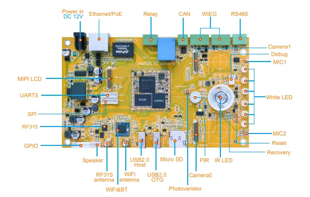
Kit fampandrosoana (Idea1126)
Torolàlana momba ny famolavolana Hardware
Reference Circuit Periferika
Circuit herinaratra lehibe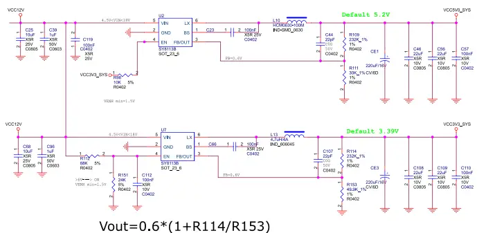
Debug Circuit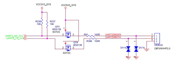
USB OTG Interface Circuit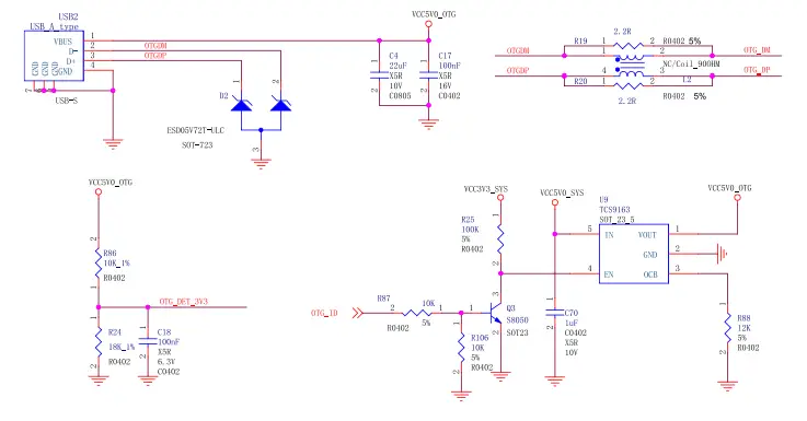
PCB footprint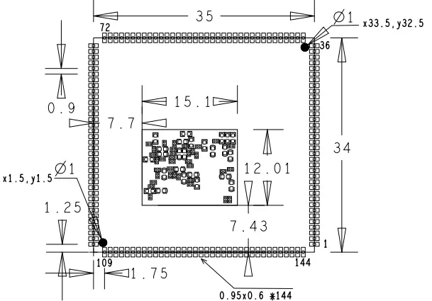
Toetra elektrika vokatra
Ny fanariana sy ny maripana
| marika famantarana | fikirana | Min | Typ | Max | Unit |
| VCC3V3_SYS | System IO
BOKYtage |
3.3-5% | 3.3 | 3.3 + 5% | V |
| Isys_in | VCC3V3_SYS fampidirana ankehitriny | 850 | mA | ||
| Ta | Temperature miasa | -20 | 70 | °C | |
| Tstg | Temperature fitehirizana | -40 | 85 | °C |
azo itokisana ny Test
| Fitsapana miasa amin'ny hafanana avo | ||
| Hevitra ato Anatiny | Operating 8h in high temperatures | 55 ° C ± 2 ° C |
| vokany | TBD |
| Fitsapana fiainana miasa | ||
| Hevitra ato Anatiny | Operating in the room | 120h |
| vokany | TBD |
Garantie voafetra
Boardcon warrants this product to be free of defects in material and workmanship for one year from the date of purchase. During this warranty period, Boardcon will repair or replace the defective unit by the following process: A copy of the original invoice must be included when returning the defective unit to Boardcon. This limited warranty does not cover damages resulting from lightning or other power surges, misuse, abuse, abnormal conditions of operation, or attempts to alter or modify the function of the product. This warranty is limited to the repair or replacement of the defective unit. In no event shall Boardcon be liable or responsible for any loss or damages, including but not limited to any lost profits, incidental or consequential damages, loss of business, or anticipatory profits arising from the use or inability to use this product. Repairs made after the expiration of the warranty period are subject to a repair charge and the cost of return shipping. Please contact Boardcon to arrange for any repair service and to obtain repair charge information.
FAQs
Q: How do I upgrade the DDR memory on CM1126B-P?
A: The CM1126B-P supports up to 4GB LPDDR4 memory. To upgrade, ensure compatibility with the specifications and follow recommended procedures.
Q: What is the power supply requirement for CM1126B-P?
A: The power requirement for CM1126B-P is DC 3.3V. Ensure to provide a stable power supply within this range for optimal performance.
Q: Can I expand the storage capacity of eMMC on CM1126B-P?
A: Yes, the eMMC storage on CM1126B-P can be expanded up to 256GB. Ensure compatibility with supported storage devices before upgrading.
Documents / Loharano
 |
Boardcon Embedded CM1126B-P System on Module [pdf] Boky Torolàlana V2.20250422, CM1126B-P System on Module, CM1126B-P, System on Module, Module |