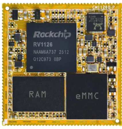
Boardcon Embedded CM1126B-P System on Module
Specifications
| Feature | Specifications |
| CPU | Quad-core Cortex-A53 |
| DDR | 2GB LPDDR4 (up to 4GB) |
| eMMC FLASH | 8GB (up to 256GB) |
| Power | DC 3.3V |
| MIPI DSI | 4-Lane |
| I2S | 4-CH |
| MIPI CSI | 2-CH 4-Lane |
| RGB LCD | 24bit |
| Camera | 1-CH(DVP) and 2-CH(CSI) |
| USB | 2-CH (USB HOST 2.0 and OTG 2.0) |
| Ethernet | 1000M GMAC |
| SDMMC | 2-CH |
| I2C | 5-CH |
| SPI | 2-CH |
| UART | 5-CH, 1-CH(DEBUG) |
| PWM | 11-CH |
| ADC IN | 4-CH |
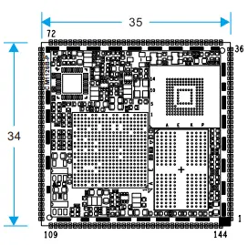
| Board Dimension | 34 x 35mm |
Introduction
About this Manual
This manual is intended to provide the user with an overview of the board and its benefits, complete feature specifications, and setup procedures. It contains important safety information as well.
Feedback and Update to this Manual
To help our customers make the most of our products, we are continually making additional and updated resources available on the Boardcon website (www.boardcon.com, www.armdesigner.com). These include manuals, application notes, programming examples, and updated software and hardware. Check in periodically to see what’s new! When we are prioritizing work on these updated resources, feedback from customers is the number one influence, If you have questions, comments, or concerns about your product or project, please no hesitate to contact us at support@armdesigner.com.
CM1126B-P Introduction
Summary
The CM1126B-P system-on-module is equipped with Rockchip’s RV1126B-P, built with a quad-core Cortex-A53, 3.0 TOPs NPU, and RISC-V MCU. It is designed specifically for the IPC/CVR devices, AI Camera devices, intelligent interactive devices, and mini robots. High-performance and low-power solutions can help customers introduce new technologies more quickly and enhance the overall solution efficiency. The smallest size can be put on a 38board. Following the hardware revision from CM1126 (V1) to CM1126B-P (V2), where the SoC is updated to the RV1126B-P, the Reset & OTG_VBUS signals and the WIFI/BT module’s GPIO voltage must operate at a 3.3V logic level.
Features
Microprocessor
- Quad-core Cortex-A53 up to 1.6GHz
- 32KB I-cache and 32KB D-cache for each core, 512KB L3 cache
- 3.0 TOPS Neural Process Unit
- RISC-V MCU to support 250ms fast boot
- Max 12M ISP
Memory Organization
- LPDDR4 RAM up to 4GB
- eMMC up to 256GB
- SPI Flash up to 8MB
Video Decoder/Encoder
- Supports video decode/encode up to 4K@30fps
- Supports real-time decoding of H.264/265
- Supports real-time UHD H.264/265 video encoding
- Picture size up to 8192×8192
Display Subsystem
- Video Output
- Supports 4 lanes MIPI DSI up to 2560×1440@60fps
- Supports 24-bit RGB parallel output
- Image in
- Supports up to 16-bit DVP interface
- Supports 2ch MIPI CSI 4lanes interface
I2S/PCM/ AC97
- Three I2S/PCM interface
- Support Mic array Up to 8ch PDM/TDM interface
- Support PWM audio output
USB and PCIE
- Two 2.0 USB interfaces
- One USB 2.0 OTG and one 2.0 USB host
Ethernet
- RTL8211F onboard
- Support 10/100/1000M
I2C
- Up to five I2Cs
- Support standard mode and fast mode(up to 400kbit/s)
SDIO
- Support 2CH SDIO 3.0 protocol
SPI
- Up to two SPI controllers,
- Full-duplex synchronous serial interface
UART
- Support up to 6 UARTs
- UART2 with 2 wires for debug tools
- Embedded two 664-byte FIFOs
- Support auto flow control mode for UART0/1/3/4/5
ADC
- Up to four ADC channels
- 12-bit resolution
- Voltage input range between 0V to 1.8V
- Support up to 1MS/s sampling rate
PWM
- 11 on-chip PWMs with interrupt-based operation
- Support 32-bit time/counter facility
- IR option on PWM3/7
Power unit
- Discrete Power on board
- Single 3.3V input
CM1126B-P Block Diagram
RV1126B-P Block Diagram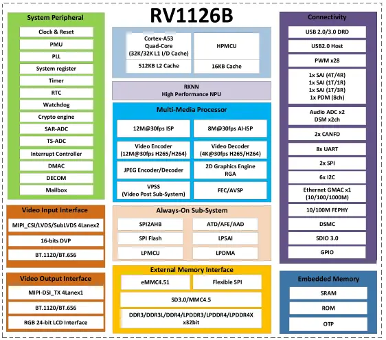
Development board (Idea1126) Block Diagram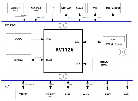
CM1126B-P PCB Dimension
CM1126B-P Pin Definition
| Pin | Signal | Description or functions | GPIO serial | IO Voltage |
| 1 | LCDC_D19_3V3 | I2S1_MCLK_M2/CIF_D15_M1 | GPIO2_C7_d | 3.3V |
| 2 | LCDC_D20_3V3 | I2S1_SDO_M2/CIF_VS_M1 | GPIO2_D0_d | 3.3V |
| 3 | LCDC_D21_3V3 | I2S1_SCLK_M2/CIF_CLKO_M1 | GPIO2_D1_d | 3.3V |
| 4 | LCDC_D22_3V3 | I2S1_LRCK_M2/CIF_CKIN_M1 | GPIO2_D2_d | 3.3V |
| 5 | LCDC_D23_3V3 | I2S1_SDI_M2/CIF_HS_M1 | GPIO2_D3_d | 3.3V |
| 6 | GND | Ground | 0V | |
| 7 | GPIO1_D1 | UART1_RX_M1/I2C5_SDA_M2 | GPIO1_D1_d | 3.3V(V2) |
| 8 | BT_WAKE | SPI0_CS1n_M0 | GPIO0_A4_u | 3.3V(V2) |
| 9 | WIFI_REG_ON | SPI0_MOSI_M0 | GPIO0_A6_d | 3.3V(V2) |
| 10 | BT_RST | SPI0_MISO_M0 | GPIO0_A7_d | 3.3V(V2) |
| 11 | WIFI_WAKE_HOST | SPI0_CLK_M0 | GPIO0_B0_d | 3.3V(V2) |
| 12 | BT_WAKE_HOST | SPI0_CS0n_M0 | GPIO0_A5_u | 3.3V(V2) |
| 13 | PWM7_IR_M0_3V3 | GPIO0_B1_d | 3.3V | |
| 14 | PWM6_M0_3V3 | TSADC_SHUT_M1 | GPIO0_B2_d | 3.3V |
| 15 | UART2_TX_3V3 | For debug | GPIO3_A2_u | 3.3V |
| 16 | UART2_RX_3V3 | For debug | GPIO3_A3_u | 3.3V |
| 17 | I2S0_MCLK_M0_3V
3 |
GPIO3_D2_d | 3.3V | |
| 18 | I2S0_SCLK_TX_M0
_3V3 |
ACODEC_DAC_CLK | GPIO3_D0_d | 3.3V |
| 19 | I2S0_SDI3_M0_3V3 | PDM_SDI3_M0 /
ACODEC_ADC_DATA |
GPIO3_D7_d | 3.3V |
| 20 | I2S0_SDO0_M0_3V
3 |
ACODEC_DAC_DATAR
/APWM_R_M1/ADSM_LP |
GPIO3_D5_d | 3.3V |
| Pin | Signal | Description or functions | GPIO serial | IO Voltage |
| 21 | I2S0_LRCK_TX_M0
_3V3 |
ACODEC_DAC_SYNC
/APWM_L_M1/ADSM_LN |
GPIO3_D3_d | 3.3V |
| 22 | PDM_SDI1_3V3 | I2S0_SDO3_SDI1_M0/I2C4SDA | GPIO4_A1_d | 3.3V |
| 23 | PDM_CLK1_3V3 | I2S0_SCK_RX_M0 | GPIO3_D1_d | 3.3V |
| 24 | PDM_SDI2_3V3 | I2S0_SDO2_SDI2_M0/I2C4SCL | GPIO4_A0_d | 3.3V |
| 25 | PDM_SDI0_3V3 | I2S0_SDI0_M0 | GPIO3_D6_d | 3.3V |
| 26 | PDM_CLK_3V3 | I2S0_LRCK_RX_M0 | GPIO3_D4_d | 3.3V |
| 27 | I2C2_SDA_3V3 | PWM5_M0 | GPIO0_C3_d | 3.3V |
| 28 | I2C2_SCL_3V3 | PWM4_M0 | GPIO0_C2_d | 3.3V |
| 29 | USB_HOST_DP | 1.8V | ||
| 30 | USB_HOST_DM | 1.8V | ||
| 31 | GND | Ground | 0V | |
| 32 | OTG_DP | Can be used for download | 1.8V | |
| 33 | OTG_DM | Can be used for download | 1.8V | |
| 34 | OTG_DET(V2) | OTG VBUS DET IN | 3.3V(V2) | |
| 35 | OTG_ID | 1.8V | ||
| 36 | SPI0_CS1n_M1 | I2S1_MCK_M1/UART4_TX_M2 | GPIO1_D5_d | 1.8V |
| 37 | VCC3V3_SYS | 3.3V Main Power input | 3.3V | |
| 38 | VCC3V3_SYS | 3.3V Main Power input | 3.3V | |
| 39 | USB_CTRL_3V3 | GPIO0_C1_d | 3.3V | |
| 40 | SDMMC0_DET | Must be used for SD Card | GPIO0_A3_u | 3.3V(V2) |
| 41 | CLKO_32K | RTC clock output | GPIO0_A2_u | 3.3V(V2) |
| 42 | nRESET | Reset key input | 3.3V(V2) | |
| 43 | MIPI_CSI_RX0_CL
KP |
MIPI CSI0 or LVDS0 input | 1.8V | |
| 44 | MIPI_CSI_RX0_CL
KN |
MIPI CSI0 or LVDS0 input | 1.8V | |
| 45 | MIPI_CSI_RX0_D2
P |
MIPI CSI0 or LVDS0 input | 1.8V | |
| 46 | MIPI_CSI_RX0_D2
N |
MIPI CSI0 or LVDS0 input | 1.8V | |
| 47 | MIPI_CSI_RX0_D3
P |
MIPI CSI0 or LVDS0 input | 1.8V | |
| 48 | MIPI_CSI_RX0_D3
N |
MIPI CSI0 or LVDS0 input | 1.8V | |
| 49 | MIPI_CSI_RX0_D1
P |
MIPI CSI0 or LVDS0 input | 1.8V | |
| 50 | MIPI_CSI_RX0_D1
N |
MIPI CSI0 or LVDS0 input | 1.8V | |
| 51 | MIPI_CSI_RX0_D0
P |
MIPI CSI0 or LVDS0 input | 1.8V |
| Pin | Signal | Description or functions | GPIO serial | IO Voltage |
| 52 | MIPI_CSI_RX0_D0
N |
MIPI CSI0 or LVDS0 input | 1.8V | |
| 53 | GND | Ground | 0V | |
| 54 | MIPI_CSI_RX1_D3
P |
MIPI CSI1 or LVDS1 input | 1.8V | |
| 55 | MIPI_CSI_RX1_D3
N |
MIPI CSI1 or LVDS1 input | 1.8V | |
| 56 | MIPI_CSI_RX1_CL
KP |
MIPI CSI1 or LVDS1 input | 1.8V | |
| 57 | MIPI_CSI_RX1_CL
KN |
MIPI CSI1 or LVDS1 input | 1.8V | |
| 58 | MIPI_CSI_RX1_D2
P |
MIPI CSI1 or LVDS1 input | 1.8V | |
| 59 | MIPI_CSI_RX1_D2
N |
MIPI CSI1 or LVDS1 input | 1.8V | |
| 60 | MIPI_CSI_RX1_D1
P |
MIPI CSI1 or LVDS1 input | 1.8V | |
| 61 | MIPI_CSI_RX1_D1
N |
MIPI CSI1 or LVDS1 input | 1.8V | |
| 62 | MIPI_CSI_RX1_D0
P |
MIPI CSI1 or LVDS1 input | 1.8V | |
| 63 | MIPI_CSI_RX1_D0
N |
MIPI CSI1 or LVDS1 input | 1.8V | |
| 64 | SDMMC0_D3_3V3 | UART3_TX_M1 | GPIO1_A7_u | 3.3V |
| 65 | SDMMC0_D2_3V3 | UART3_RX_M1 | GPIO1_A6_u | 3.3V |
| 66 | SDMMC0_D1_3V3 | UART2_TX_M0 | GPIO1_A5_u | 3.3V |
| 67 | SDMMC0_D0_3V3 | UART2_RX_M0 | GPIO1_A4_u | 3.3V |
| 68 | SDMMC0_CMD_3V
3 |
UART3_CTSn_M1 | GPIO1_B1_u | 3.3V |
| 69 | SDMMC0_CLK_3V3 | UART3_RTSn_M1 | GPIO1_B0_u | 3.3V |
| 70 | GND | Ground | 0V | |
| 71 | LED1/CFG_LDO0 | Ethernet LINK LED | 3.3V | |
| 72 | LED2/CFG_LDO1 | Ethernet SPEED LED | 3.3V | |
| 73 | MDI0+ | Ethernet MDI signal | 1.8V | |
| 74 | MDI0- | Ethernet MDI signal | 1.8V | |
| 75 | MDI1+ | Ethernet MDI signal | 1.8V | |
| 76 | MDI1- | Ethernet MDI signal | 1.8V | |
| 77 | MDI2+ | Ethernet MDI signal | 1.8V | |
| 78 | MDI2- | Ethernet MDI signal | 1.8V | |
| 79 | MDI3+ | Ethernet MDI signal | 1.8V | |
| 80 | MDI3- | Ethernet MDI signal | 1.8V | |
| 81 | I2C1_SCL | UART4_CTSn_M2 | GPIO1_D3_u | 1.8V |
| Pin | Signal | Description or functions | GPIO serial | IO Voltage |
| 82 | I2C1_SDA | UART4_RTSn_M2 | GPIO1_D2_u | 1.8V |
| 83 | MIPI_CSI_PWDN0 | UART4_RX_M2 | GPIO1_D4_d | 1.8V |
| 84 | SPI0_CLK_M1 | I2S1_SDO_M1/UART5_RX_M2 | GPIO2_A1_d | 1.8V |
| 85 | SPI0_MOSI_M1 | I2S1_SCK_M1/I2C3_SCL_M2 | GPIO1_D6_d | 1.8V |
| 86 | SPI0_CS0n_M1 | I2S1_SDI_M1/UART5_TX_M2 | GPIO2_A0_d | 1.8V |
| 87 | SPI0_MISO_M1 | I2S1_LRCK_M1/I2C3_SDA_M2 | GPIO1_D7_d | 1.8V |
| 88 | MIPI_CSI_CLK1 | UART5_RTSn_M2 | GPIO2_A2_d | 1.8V |
| 89 | MIPI_CSI_CLK0 | UART5_CTSn_M2 | GPIO2_A3_d | 1.8V |
| 90 | GND | Ground | 0V | |
| 91 | LCDC_D0_3V3 | UART4_RTSn_M1/CIF_D0_M1 | GPIO2_A4_d | 3.3V |
| 92 | LCDC_D1_3V3 | UART4_CTSn_M1/CIF_D1_M1 | GPIO2_A5_d | 3.3V |
| 93 | LCDC_D2_3V3 | UART4_TX_M1/CIF_D2_M1 | GPIO2_A6_d | 3.3V |
| 94 | LCDC_D3_3V3 | UART4_RX_M1/I2S2_SDO_M1 | GPIO2_A7_d | 3.3V |
| 95 | LCDC_D4_3V3 | UART5_TX_M1/I2S2_SDI_M1 | GPIO2_B0_d | 3.3V |
| 96 | LCDC_D5_3V3 | UART5_RX_M1/I2S2_SCK_M1 | GPIO2_B1_d | 3.3V |
| 97 | LCDC_D6_3V3 | UART5_RTSn_M1/I2S2_LRCK_
M1 |
GPIO2_B2_d | 3.3V |
| 98 | LCDC_D7_3V3 | UART5_CTSn_M1/I2S2_MCLK_
M1/CIF_D3_M1 |
GPIO2_B3_d | 3.3V |
| 99 | CAN_RX_3V3 | UART3_TX_M2/I2C4_SCL_M0 | GPIO3_A0_u | 3.3V |
| 100 | CAN_TX_3V3 | UART3_RX_M2/I2C4_SDA_M0 | GPIO3_A1_u | 3.3V |
| 101 | LCDC_CLK_3V3 | UART3_CTSn_M2/SPI1_MISO_
M2/PWM8_M1 |
GPIO2_D7_d | 3.3V |
| 102 | LCDC_VSYNC_3V3 | UART3_RTSn_M2/SPI1_MOSI | GPIO2_D6_d | 3.3V |
| 103 | MIPI_DSI_D2P | 1.8V | ||
| 104 | MIPI_DSI_D2N | 1.8V | ||
| 105 | MIPI_DSI_D1P | 1.8V | ||
| 106 | MIPI_DSI_D1N | 1.8V | ||
| 107 | MIPI_DSI_D0P | 1.8V | ||
| 108 | MIPI_DSI_D0N | 1.8V | ||
| 109 | MIPI_DSI_D3P | 1.8V | ||
| 110 | MIPI_DSI_D3N | 1.8V | ||
| 111 | MIPI_DSI_CLKP | 1.8V | ||
| 112 | MIPI_DSI_CLKN | 1.8V | ||
| 113 | ADCIN3 | ADC input | 1.8V | |
| 114 | ADCIN2 | ADC input | 1.8V | |
| 115 | ADCIN1 | ADC input | 1.8V | |
| 116 | ADKEY_IN0 | Recovery mode set(10K PU) | 1.8V | |
| 117 | GND | Ground | 0V | |
| 118 | SDIO_CLK | GPIO1_B2_d | 3.3V(V2) | |
| 119 | SDIO_CMD | GPIO1_B3_u | 3.3V(V2) |
| Pin | Signal | Description or functions | GPIO serial | IO Voltage |
| 120 | SDIO_D0 | GPIO1_B4_u | 3.3V(V2) | |
| 121 | SDIO_D1 | GPIO1_B5_u | 3.3V(V2) | |
| 122 | SDIO_D2 | GPIO1_B6_u | 3.3V(V2) | |
| 123 | SDIO_D3 | GPIO1_B7_u | 3.3V(V2) | |
| 124 | UART0_RX | GPIO1_C2_u | 3.3V(V2) | |
| 125 | UART0_TX | GPIO1_C3_u | 3.3V(V2) | |
| 126 | UART0_CTSN | GPIO1_C1_u | 3.3V(V2) | |
| 127 | UART0_RTSN | GPIO1_C0_u | 3.3V(V2) | |
| 128 | PCM_TX | I2S2_SDO_M0/SPI1_MOSI_M1 | GPIO1_C4_d | 3.3V(V2) |
| 129 | PCM_SYNC | I2S2_LRCK_M0/SPI1_CSn0_M
1/UART1_CTSn_M1 |
GPIO1_C7_d | 3.3V(V2) |
| 130 | PCM_CLK | I2S2_SCLK_M0/SPI1_CLK_M1/
UART1_RTSn_M1 |
GPIO1_C6_d | 3.3V(V2) |
| 131 | PCM_RX | I2S2_SDI_M0/SPI1_MISO_M1 | GPIO1_C5_d | 3.3V(V2) |
| 132 | LCDC_D15_3V3 | CIF_D11_M1 | GPIO2_C3_d | 3.3V |
| 133 | LCDC_D14_3V3 | CIF_D10_M1 | GPIO2_C2_d | 3.3V |
| 134 | LCDC_D13_3V3 | CIF_D9_M1 | GPIO2_C1_d | 3.3V |
| 135 | LCDC_D12_3V3 | CIF_D8_M1 | GPIO2_C0_d | 3.3V |
| 136 | LCDC_DEN_3V3 | I2C3_SCL_M1/SPI1_CS0n_M2 | GPIO2_D4_d | 3.3V |
| 137 | LCDC_D10_3V3 | CIF_D6_M1 | GPIO2_B6_d | 3.3V |
| 138 | LCDC_D9_3V3 | CIF_D5_M1 | GPIO2_B5_d | 3.3V |
| 139 | LCDC_D8_3V3 | CIF_D4_M1 | GPIO2_B4_d | 3.3V |
| 140 | LCDC_D11_3V3 | CIF_D7_M1 | GPIO2_B7_d | 3.3V |
| 141 | LCDC_HSYNC_3V3 | I2C3_SDA_M1/SPI1_CLK_M2 | GPIO2_D5_d | 3.3V |
| 142 | LCDC_D16_3V3 | CIF_D12_M1 | GPIO2_C4_d | 3.3V |
| 143 | LCDC_D17_3V3 | CIF_D13_M1 | GPIO2_C5_d | 3.3V |
| 144 | LCDC_D18_3V3 | CIF_D14_M1 | GPIO2_C6_d | 3.3V |
| Note:
1. Most GPIO voltage is 1.8V, but some pins marked 3.3V. 2. GPIO voltage change to 3.3V for marked (V2). |
||||
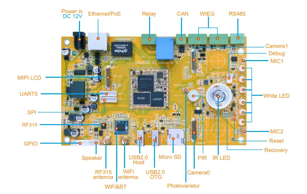
Development Kit (Idea1126)
Hardware Design Guide
Peripheral Circuit Reference
Main Power Circuit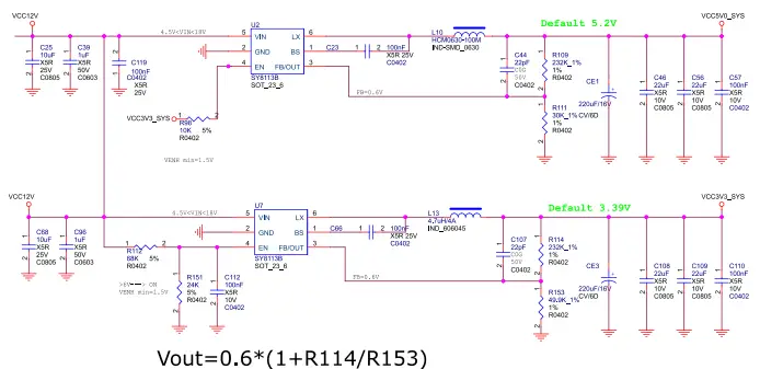
Debug Circuit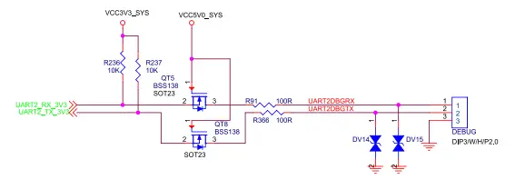
USB OTG Interface Circuit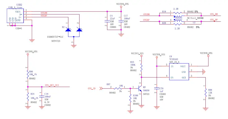
PCB Footprint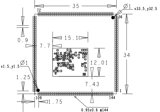
Product Electrical Characteristics
Dissipation and Temperature
| Symbol | Parameter | Min | Typ | Max | Unit |
| VCC3V3_SYS | System IO
Voltage |
3.3-5% | 3.3 | 3.3+5% | V |
| Isys_in | VCC3V3_SYS input Current | 850 | mA | ||
| Ta | Operating Temperature | -20 | 70 | °C | |
| Tstg | Storage Temperature | -40 | 85 | °C |
Reliability of Test
| High Temperature Operating Test | ||
| Contents | Operating 8h in high temperatures | 55°C±2°C |
| Result | TBD |
| Operating Life Test | ||
| Contents | Operating in the room | 120h |
| Result | TBD |
Limited Warranty
Boardcon warrants this product to be free of defects in material and workmanship for one year from the date of purchase. During this warranty period, Boardcon will repair or replace the defective unit by the following process: A copy of the original invoice must be included when returning the defective unit to Boardcon. This limited warranty does not cover damages resulting from lightning or other power surges, misuse, abuse, abnormal conditions of operation, or attempts to alter or modify the function of the product. This warranty is limited to the repair or replacement of the defective unit. In no event shall Boardcon be liable or responsible for any loss or damages, including but not limited to any lost profits, incidental or consequential damages, loss of business, or anticipatory profits arising from the use or inability to use this product. Repairs made after the expiration of the warranty period are subject to a repair charge and the cost of return shipping. Please contact Boardcon to arrange for any repair service and to obtain repair charge information.
FAQs
Q: How do I upgrade the DDR memory on CM1126B-P?
A: The CM1126B-P supports up to 4GB LPDDR4 memory. To upgrade, ensure compatibility with the specifications and follow recommended procedures.
Q: What is the power supply requirement for CM1126B-P?
A: The power requirement for CM1126B-P is DC 3.3V. Ensure to provide a stable power supply within this range for optimal performance.
Q: Can I expand the storage capacity of eMMC on CM1126B-P?
A: Yes, the eMMC storage on CM1126B-P can be expanded up to 256GB. Ensure compatibility with supported storage devices before upgrading.
Documents / Resources
 |
Boardcon Embedded CM1126B-P System on Module [pdf] User Manual V2.20250422, CM1126B-P System on Module, CM1126B-P, System on Module, Module |