![]() CC1312PSIP
CC1312PSIP
SWRS293 – MAY 2023
CC1312PSIP SimpleLink™ Sub-1-GHz Wireless System-in-Package
Features
Wireless microcontroller
- Powerful 48-MHz Arm ® Cortex ® TI Co nfid -M4F processor
- 352KB flash program memory
- 256KB of ROM for protocols and library functions
- 8KB of cache SRAM
- 80KB of ultra-low leakage SRAM with parity for high-reliability operation
- Dynamic multiprotocol manager (DMM) driver
- Programmable radio includes support for 2(G)FSK, 4-(G)FSK, MSK, OOK, IEEE 802.15.4 PHY and MAC
- Supports over-the-air upgrade (OTA) Ultra-low power sensor controller
- Autonomous MCU with 4KB of SRAM
- Sample, store, and process sensor data
- Fast wake-up for low-power operation
- Software defined peripherals; capacitive touch, flow meter,
LCD Low power consumption - MCU consumption: – 2.9 mA active mode, CoreMark ®
– 60 μA/MHz running CoreMark®
– 0.9 μA standby mode, RTC, 80KB RAM
– 0.1 μA shutdown mode, wake-up on pin - Ultra low-power sensor controller consumption:
– 30 μA in 2-MHz mode
– 808 μA in 24-MHz mode - Radio Consumption:
– 5.8-mA RX at 868 MHz
– 28.7-mA TX at +14 dBm at 868 MHz
Wireless protocol support - Wi-SUN®
- mioty®
- Wireless M-Bus
- SimpleLink™ TI 15.4-stack
- 6LoWPAN
- Proprietary systems High-performance radio
- –119 dBm for 2.5-kbps long-range mode
- –108 dBm at 50 kbps, 802.15.4, 868 MHz
Regulatory compliance - Pre-certified for:
– FCC CFR47 Part 15 - Suitable for systems targeting compliance with:
– ETSI EN 300 220 Receiver Cat. 1.5 and 2, EN 303 131, EN 303 204
– ARIB STD-T108
MCU peripherals - Digital peripherals can be routed to 30 GPIOs
- Four 32-bit or eight 16-bit general-purpose timers
- 12-bit ADC, 200 kSamples/s, 8 channels
- 8-bit DAC
- Two comparators
- Programmable current source
- Two UART, two SSI, I
- Real-time clock (RTC)
- Integrated temperature and battery monitor
Security enablers - AES 128- and 256-bit cryptographic accelerator
- ECC and RSA public key hardware accelerator
- SHA2 Accelerator (full suite up to SHA-512)
- True random number generator (TRNG)
Development tools and software - LP-CC1312PSIP Development Kit
- SimpleLink™ CC13xx and CC26xx Software
Development Kit (SDK) - SmartRF™ Studio for simple radio configuration
- Sensor Controller Studio for building low-power sensing applications
- SysConfig system configuration tool
Operating range - 1.8-V to 3.8-V single supply voltage
- –40 to +105°C (+14 dBm PA)
All necessary components integrated - 48-MHz crystal: RF accuracy ±10 ppm
- 32-kHz crystal: RTC accuracy ±50 ppm
- DC/DC converter components and decoupling capacitors
- RF front-end components with 50-Ohm output
Package - 7-mm × 7-mm MOT (30 GPIOs)
- Pin-to-pin compatible with CC2652RSIP and CC2652PSIP
- RoHS-compliant package
![]() IMPORTANT NOTICE at the end of this data sheet addresses availability, warranty, changes, use in safety-critical applications, intellectual property matters and other important disclaimers. ADVANCE INFORMATION for preproduction products; subject to change without notice.
IMPORTANT NOTICE at the end of this data sheet addresses availability, warranty, changes, use in safety-critical applications, intellectual property matters and other important disclaimers. ADVANCE INFORMATION for preproduction products; subject to change without notice.
Applications
- 868 and 902 to 928 MHz ISM and SRD systems 1 with down to 4 kHz of receive bandwidth
- Building automation
– Building security systems – motion detector, electronic smart lock, door and window sensor, garage door system, gateway
– HVAC – thermostat, wireless environmental sensor, HVAC system controller, gateway
– Fire safety system – smoke and heat detector, fire alarm control panel (FACP)
– Video surveillance – IP network camera
– Elevators and escalators – elevator main control panel for elevators and escalators - Grid infrastructure
– Smart meters – water meter, gas meter, electricity meter, and heat cost allocators
– Grid communications – wireless communications – long-range sensor applications
– EV Charging infrastructure – AC charging (pile) station
– Other alternative energy – energy harvesting - Industrial transport – asset tracking
- Factory automation and control
- Medical
- Communication equipment
– Wired networking – wireless LAN or Wi-Fi access points, edge router
Description
The SimpleLink ™ CC1312PSIP device is a System-in-Package (SiP) Sub-1 GHz wireless module supporting IEEE 802.15.4, IPv6-enabled smart objects (6LoWPAN), mioty, proprietary systems, including the TI 15.4-Stack. The CC1312PSIP microcontroller (MCU) is based on an Arm M4F main processor and optimized for low-power wireless communication and advanced sensing in grid infrastructure, building automation, retail automation and medical applications. The CC1312PSIP has a low sleep current of 0.9 μA with RTC and 80KB RAM retention. In addition to the main Cortex® M4F processor, the device also has an autonomous ultra-low power Sensor Controller CPU with fast wake-up capability. As an example, the sensor controller is capable of 1-Hz ADC sampling at average 1-μA system current.
The CC1312PSIP has Low SER (Soft Error Rate) FIT (Failure-in-time) for long operational lifetime. Always-on SRAM parity minimizes risk for corruption due to potential radiation events. Consistent with many customers’ 10 to 15 years or longer life cycle requirements, TI has a product life cycle policy with a commitment to product longevity and continuity of supply including dual sourcing of key components in the SIP. The CC1312PSIP device is part of the SimpleLink™ MCU platform, which consists of Wi-Fi®, Bluetooth® Low Energy, Thread, Zigbee, Wi-SUN®, Amazon Sidewalk, mioty, Sub-1 GHz MCUs, and host MCUs. CC1312PSIP is part of a portfolio that includes pin-compatible 2.4-GHz SIPs for easy adaption of a wireless product to multiple communication standards. The common SimpleLink™CC13xx and CC26xx Software Development Kit (SDK) and SysConfig system configuration tool supports migration between devices in the portfolio. A comprehensive number of software stacks, application examples and SimpleLink Academy training sessions are included in the SDK. For more information, visit wireless connectivity.
| PART NUMBER | PACKAGE | BODY SIZE (NOM) |
| CC1312PSIPMOT | QFM | 7.00 mm × 7.00 mm |
(1) For the most current part, package, and ordering information for all available devices, see the Package Option Addendum in Mechanical, Packaging, and Orderable Information, or see the TI website.
1 See RF Core for additional details on supported protocol standards, modulation formats, and data rates.
Functional Block Diagram
Revision History
NOTE: Page numbers for previous revisions may differ from page numbers in the current version.
| DATE | REVISION | NOTES |
| May-23 | * | Initial Release |
Device Comparison
Pin Configuration and Functions
7.1 Pin Diagram – MOT Package (Top View)
Figure 7-1. MOT (7-mm × 7-mm) Pinout, 0.5-mm Pitch (Top View)
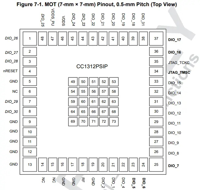
The following I/O pins marked in Figure 7-1 in bold have high-drive capabilities:
- Pin 23, DIO_5
- Pin 24, DIO_6
- Pin 25, DIO_7
- Pin 34, JTAG_TMSC
- Pin 36, DIO_16
- Pin 37, DIO_17
The following I/O pins marked in Figure 7-1 in italics have analog capabilities:
- Pin 1, DIO_26
- Pin 2, DIO_27
- Pin 3, DIO_28
- Pin 7, DIO_29
- Pin 8, DIO_30
- Pin 44, DIO_23
- Pin 45, DIO_24
- Pin 48, DIO_25
7.2 Signal Descriptions – MOT Package
Table 7-1. Signal Descriptions – SIP Package
| PIN | I/O | TYPE |
DESCRIPTION |
|
| NAME |
NO. |
|||
| NC | 14 | I/O | Digital | No Connect |
| DIO_1 | 21 | I/O | Digital | GPIO |
| DIO_10 | 28 | I/O | Digital | GPIO |
| DIO_11 | 29 | I/O | Digital | GPIO |
| DIO_12 | 30 | I/O | Digital | GPIO |
| DIO_13 | 31 | I/O | Digital | GPIO |
| DIO_14 | 32 | I/O | Digital | GPIO |
| DIO_15 | 33 | I/O | Digital | GPIO |
| DIO_16 | 36 | I/O | Digital | GPIO, JTAG_TDO, high-drive capability |
| DIO_17 | 37 | I/O | Digital | GPIO, JTAG_TDI, high-drive capability |
| DIO_18 | 39 | I/O | Digital | GPIO |
| DIO_19 | 40 | I/O | Digital | GPIO |
| DIO_2 | 20 | I/O | Digital | GPIO |
| DIO_20 | 41 | I/O | Digital | GPIO |
| DIO_21 | 42 | I/O | Digital | GPIO |
| DIO_22 | 43 | I/O | Digital | GPIO |
| DIO_23 | 44 | I/O | Digital or Analog | GPIO, analog capability |
| DIO_24 | 45 | I/O | Digital or Analog | GPIO, analog capability |
| DIO_25 | 48 | I/O | Digital or Analog | GPIO, analog capability |
| DIO_26 | 1 | I/O | Digital or Analog | GPIO, analog capability |
| DIO_27 | 2 | I/O | Digital or Analog | GPIO, analog capability |
| DIO_28 | 3 | I/O | Digital or Analog | GPIO, analog capability |
| DIO_29 | 7 | I/O | Digital or Analog | GPIO, analog capability |
| NC | 15 | I/O | Digital | No Connect |
| DIO_30 | 8 | I/O | Digital or Analog | GPIO, analog capability |
| PIO_31 | 38 | I/O | Digital | Supports only peripheral functionality. Does not support general purpose I/O functionality. |
| DIO_4 | 22 | I/O | Digital | GPIO |
| DIO_5 | 23 | I/O | Digital | GPIO, high-drive capability |
| DIO_6 | 24 | I/O | Digital | GPIO, high-drive capability |
| DIO_7 | 25 | I/O | Digital | GPIO, high-drive capability |
| DIO_8 | 26 | I/O | Digital | GPIO |
| DIO_9 | 27 | I/O | Digital | GPIO |
| GND | 5 | — | — | GND |
| GND | 9 | — | — | GND |
| GND | 10 | — | — | GND |
| GND | 11 | — | — | GND |
| GND | 12 | — | — | GND |
| GND | 13 | — | — | GND |
| GND | 16 | — | — | GND |
| GND | 17 | — | — | GND |
| GND | 19 | — | — | GND |
| GND | 49-73 | — | — | GND |
7.3 Connections for Unused Pins and Modules
Table 7-2. Connections for Unused Pins
| PIN | I/O | TYPE |
DESCRIPTION |
|
|
NAME |
NO. |
|||
| NC | 6 | — | — | No Connect |
| nRESET | 4 | I | Digital | Reset, active low. Internal pullup resistor and internal 100 nF to VDDS_PU |
| RF | 18 | — | RF | 50 ohm RF port |
| JTAG_TCKC | 35 | I | Digital | JTAG_TCKC |
| JTAG_TMSC | 34 | I/O | Digital | JTAG_TMSC, high-drive capability |
| VDDS | 46 | — | Power | 1.8-V to 3.8-V main SIP supply |
| VDDS_PU | 47 | — | Power | Power to reset internal pullup resistor |
Specifications
8.1 Absolute Maximum Ratings
over operating free-air temperature range (unless otherwise noted)(1) (2)
|
|
MIN | MAX |
UNIT |
||
| VDDS(3) | Supply voltage | –0.3 | 4.1 | V | |
| Voltage on any digital pin(4) | –0.3 | VDDS + 0.3, max 4.1 | V | ||
| Vin | Voltage on ADC input | Voltage scaling enabled | –0.3 | VDDS |
V |
| Voltage scaling disabled, internal reference | –0.3 | 1.49 | |||
| Voltage scaling disabled, VDDS as reference | –0.3 | VDDS / 2.9 | |||
| 10 | dBm | ||||
| Tstg | Storage temperature | –40 | 150 | °C | |
- Operation outside the Absolute Maximum Ratings may cause permanent device damage. Absolute Maximum Ratings do not imply functional operation of the device at these or any other conditions beyond those listed under Recommended Operating Conditions. If used outside the Recommended Operating Conditions but within the Absolute Maximum Ratings, the device may not be fully functional, and this may affect device reliability, functionality, performance, and shorten the device lifetime
- All voltage values are with respect to ground, unless otherwise noted.
- VDDS_DCDC, VDDS2 and VDDS3 must be at the same potential as VDDS.
- Including analog capable DIOs.
8.2 ESD Ratings
| VALUE | UNIT | ||||
| VESD | Electrostatic discharge | Human body model (HBM), per ANSI/ESDA/JEDEC JS-001(1) | All pins | ±1000 | V |
| Charged device model (CDM), per ANSI/ESDA/JEDEC JS-002(2) | All pins | ±500 | V | ||
- JEDEC document JEP155 states that 500-V HBM allows safe manufacturing with a standard ESD control process.
- JEDEC document JEP157 states that 250-V CDM allows safe manufacturing with a standard ESD control process.
8.3 Recommended Operating Conditions
over operating free-air temperature range (unless otherwise noted)
|
|
MIN | MAX |
UNIT |
|
| Operating ambient temperature(1) (2) | –40 | 105 | °C | |
| Operating supply voltage (VDDS) | 1.8 | 3.8 | V | |
| Operating supply voltage (VDDS), boost mode | VDDR = 1.95 V +14 dBm RF output sub-1 GHz power amplifier | 2.1 | 3.8 | V |
| Rising supply voltage slew rate | 0 | 100 | mV/µs | |
| Falling supply voltage slew rate | 0 | 20 | mV/µs | |
(1) Operation at or near maximum operating temperature for extended durations will result in a reduction in lifetime.
(2) For thermal resistance characteristics refer to .
8.4 Power Supply and Modules
over operating free-air temperature range (unless otherwise noted)
|
PARAMETER |
MIN | TYP | MAX |
UNIT |
|
| VDDS Power-on-Reset (POR) threshold | 1.1 – 1.55 | V | |||
| VDDS Brown-out Detector (BOD) (1) | Rising threshold | 1.77 | V | ||
| VDDS Brown-out Detector (BOD), before initial boot (2) | Rising threshold | 1.70 | V | ||
| VDDS Brown-out Detector (BOD) (1) | Falling threshold | 1.75 | V | ||
(1) For boost mode (VDDR =1.95 V), TI drivers software initialization will trim VDDS BOD limits to maximum (approximately 2.0 V)
(2) Brown-out Detector is trimmed at initial boot, value is kept until device is reset by a POR reset or the RESET_N pin
8.5 Power Consumption – Power Modes
When measured on the CC1312PSIP-EM reference design with Tc = 25 °C, VDDS = 3.6 V with DC/DC enabled unless otherwise noted.
|
PARAMETER |
TEST CONDITIONS | TYP | UNIT | |
|
Core Current Consumption |
||||
| Icore | Reset | Reset. RESET_N pin asserted or VDDS below power-on-reset threshold (4) | 36 | µA |
| Shutdown | Shutdown. No clocks running, no retention | 150 | nA | |
| Standby with cache retention | RTC running, CPU, 80KB RAM and (partial) register retention. RCOSC_LF | 0.9 | µA | |
| RTC running, CPU, 80KB RAM and (partial) register retention XOSC_LF | 1.0 | |||
| Standby with cache retention | RTC running, CPU, 80KB RAM and (partial) register retention XOSC_LF | 2.8 | µA | |
| RTC running, CPU, 80KB RAM and (partial) register retention XOSC_LF | 2.9 | |||
| Idle | Supply Systems and RAM powered RCOSC_HF | 590 | µA | |
| Icore | Active | MCU running CoreMark at 48 MHz RCOSC_HF | 2.89 | mA |
| Peripheral Current Consumption | ||||
| Iperi | Peripheral power domain | Delta current with domain enabled | 82 | µA |
| Serial power domain | Delta current with domain enabled | 5.5 | ||
| RF Core | Delta current with power domain enabled, clock enabled, RF core idle | 179 | ||
| µDMA | Delta current with clock enabled, module is idle | 54 | ||
| Timers | Delta current with clock enabled, module is idle(3) | 68 | ||
| I2C | Delta current with clock enabled, module is idle | 8.2 | ||
| I2S | Delta current with clock enabled, module is idle | 22 | ||
| SSI | Delta current with clock enabled, module is idle(2) | 70 | ||
| UART | Delta current with clock enabled, module is idle(1) | 141 | ||
| CRYPTO (AES) | Delta current with clock enabled, module is idle | 21 | ||
| PKA | Delta current with clock enabled, module is idle | 71 | ||
| TRNG | Delta current with clock enabled, module is idle | 30 | ||
| Sensor Controller Engine Consumption | ||||
| ISCE | Active mode | 24 MHz, infinite loop | 808 | µA |
| Low-power mode | 2 MHz, infinite loop | 30.1 | ||
- Only one UART running
- Only one SSI running
- Only one GPTimer running
- CC1312PSIP integrates a 100 kΩ pull-up resistor on nRESET
8.6 Power Consumption – Radio Modes
When measured on the CC1312PSIP-EM reference design with Tc = 25 °C, VDDS = 3.6 V with DC/DC enabled unless otherwise noted.
Using boost mode (increasing VDDR up to 1.95 V), will increase system current by 15% (does not apply to TX +14 dBm setting where this current is already included).
Relevant Icore and Iperi currents are included in below numbers.
|
PARAMETER |
TEST CONDITIONS | TYP |
UNIT |
|
| Radio receive current, 868 MHz | 5.8 | mA | ||
| Radio transmit current Regular PA | 0 dBm output power setting 868 MHz | 9.4 | mA | |
| +10 dBm output power setting 868 MHz | 17.3 | mA | ||
| Radio transmit current Boost mode, regular PA | +14 dBm output power setting 868 MHz | 28.7 | mA | |
8.7 Nonvolatile (Flash) Memory Characteristics
Over operating free-air temperature range and VDDS = 3.0 V (unless otherwise noted)
| PARAMETER | TEST CONDITIONS | MIN | TYP | MAX |
UNIT |
| Flash sector size | 8 | KB | |||
| Supported flash erase cycles before failure, single-bank(1) (5) | 30 | k Cycles | |||
| Supported flash erase cycles before failure, single sector(2) | 60 | k Cycles | |||
| Maximum number of write operations per row before sector erase(3) | 83 | Write Operations | |||
| Flash retention | 105 °C | 11.4 | Years at 105°C | ||
| Flash sector erase current | Average delta current | 10.7 | mA | ||
| Flash sector erase time(4) | Zero cycles | 10 | ms | ||
| 30k cycles | 4000 | ms | |||
| Flash write current | Average delta current, 4 bytes at a time | 6.2 | mA | ||
| Flash write time(4) | 4 bytes at a time | 21.6 | µs | ||
- A full bank erase is counted as a single erase cycle on each sector.
- Up to 4 customer-designated sectors can be individually erased an additional 30k times beyond the baseline bank limitation of 30k cycles
- Each wordline is 2048 bits (or 256 bytes) wide. This limitation corresponds to sequential memory writes of 4 (3.1) bytes minimum per write over a whole wordline. If additional writes to the same wordline are required, a sector erase is required once the maximum number of write operations per row is reached.
- This number is dependent on Flash aging and increases over time and erase cycles
- Aborting flash during erase or program modes is not a safe operation.
8.8 Thermal Resistance Characteristics
| THERMAL METRIC | PACKAGE | UNIT | |
| MOT (SIP) | |||
| 73 PINS | |||
| RθJA | Junction-to-ambient thermal resistance | 48.7 | °C/W(1) |
| RθJC(top) | Junction-to-case (top) thermal resistance | 12.4 | °C/W(1) |
| RθJB | Junction-to-board thermal resistance | 32.2 | °C/W(1) |
| ψJT | Junction-to-top characterization parameter | 0.40 | °C/W(1) |
| ψJB | Junction-to-board characterization parameter | 32.0 | °C/W(1) |
(1) °C/W = degrees Celsius per watt.
8.9 RF Frequency Bands
Over operating free-air temperature range (unless otherwise noted).
| PARAMETER | MIN | TYP | MAX | UNIT |
| Frequency band | 863 | 930 | MHz |
8.10 861 MHz to 1054 MHz – Receive (RX)
When measured on the CC1312PSIP-EM reference design with Tc = 25 °C, VDDS = 3.0 V with DC/DC enabled and high power PA connected to VDDS unless otherwise noted.
All measurements are performed at the antenna input with a combined RX and TX path, except for high power PA which is measured at a dedicated antenna connection. All measurements are performed conducted.
|
PARAMETER |
TEST CONDITIONS | MIN | TYP | MAX | UNIT |
|
General Parameters |
|||||
| Digital channel filter programmable receive bandwidth | 4 | 4000 | kHz | ||
| Data rate step size | 1.5 | bps | |||
| Spurious emissions 25 MHz to 1 GHz | 868 MHz Conducted emissions measured according to ETSI EN 300 220 | < -57 | dBm | ||
| Spurious emissions 1 GHz to 13 GHz | < -47 | dBm | |||
| 802.15.4, 50 kbps, ±25 kHz deviation, 2-GFSK, 100 kHz RX Bandwidth | |||||
| Sensitivity | BER = 10–2, 868 MHz | –108 | dBm | ||
| Saturation limit | BER = 10–2, 868 MHz | 10 | dBm | ||
| Selectivity, ±200 kHz | BER = 10–2, 868 MHz(1) | 44 | dB | ||
| Selectivity, ±400 kHz | BER = 10–2, 868 MHz(1) | 48 | dB | ||
| Blocking, ±1 MHz | BER = 10–2, 868 MHz(1) | 57 | dB | ||
| Blocking, ±2 MHz | BER = 10–2, 868 MHz(1) | 62 | dB | ||
| Blocking, ±5 MHz | BER = 10–2, 868 MHz(1) | 68 | dB | ||
| Blocking, ±10 MHz | BER = 10–2, 868 MHz(1) | 76 | dB | ||
| Image rejection (image compensation enabled) | BER = 10–2, 868 MHz(1) | 39 | dB | ||
| RSSI dynamic range | Starting from the sensitivity limit | 95 | dB | ||
| RSSI accuracy | Starting from the sensitivity limit across the given dynamic range | ±3 | dB | ||
| 802.15.4, 100 kbps, ±25 kHz deviation, 2-GFSK, 137 kHz RX Bandwidth | |||||
| Sensitivity 100 kbps | 868 MHz, 1% PER, 127 byte payload | -101 | dBm | ||
| Selectivity, ±200 kHz | 868 MHz, 1% PER, 127 byte payload. Wanted signal at -96 dBm | 38 | dB | ||
| Selectivity, ±400 kHz | 868 MHz, 1% PER, 127 byte payload. Wanted signal at -96 dBm | 45 | dB | ||
| Co-channel rejection | 868 MHz, 1% PER, 127 byte payload. Wanted signal at -79 dBm | -9 | dB | ||
| 802.15.4, 200 kbps, ±50 kHz deviation, 2-GFSK, 311 kHz RX Bandwidth | |||||
| Sensitivity | BER = 10–2, 868 MHz | –103 | dBm | ||
| Sensitivity | BER = 10–2, 915 MHz | –103 | dBm | ||
| Selectivity, ±400 kHz | BER = 10–2, 915 MHz. Wanted signal 3 dB above sensitivity limit. | 41 | dB | ||
| Selectivity, ±800 kHz | BER = 10–2, 915 MHz. Wanted signal 3 dB above sensitivity limit. | 47 | dB | ||
| Blocking, ±2 MHz | BER = 10–2, 915 MHz. Wanted signal 3 dB above sensitivity limit. | 55 | dB | ||
| Blocking, ±10 MHz | BER = 10–2, 915 MHz. Wanted signal 3 dB above sensitivity limit. | 67 | dB | ||
| 802.15.4, 500 kbps, ±190 kHz deviation, 2-GFSK, 655 kHz RX Bandwidth | |||||
| Sensitivity 500 kbps | 916 MHz, 1% PER, 127 byte payload | -90 | dBm | ||
| Selectivity, ±1 MHz | 916 MHz, 1% PER, 127 byte payload. Wanted signal at -88 dBm | 11 | dB | ||
| Selectivity, ±2 MHz | 916 MHz, 1% PER, 127 byte payload. Wanted signal at -88 dBm | 43 | dB | ||
| Co-channel rejection | 916 MHz, 1% PER, 127 byte payload. Wanted signal at -71 dBm | -9 | dB | ||
|
SimpleLink™ Long Range 2.5 kbps or 5 kbps (20 ksym/s, 2-GFSK, ±5 kHz Deviation, FEC (Half Rate), DSSS = 1:2 or 1:4, 34 kHz RX Bandwidth |
|||||
| Sensitivity | 2.5 kbps, BER = 10–2, 868 MHz | -119 | dBm | ||
| Sensitivity | 5 kbps, BER = 10–2, 868 MHz | -117 | dBm | ||
| Saturation limit | 2.5 kbps, BER = 10–2, 868 MHz | 10 | dBm | ||
| Selectivity, ±100 kHz | 2.5 kbps, BER = 10–2, 868 MHz(1) | 49 | dB | ||
| Selectivity, ±200 kHz | 2.5 kbps, BER = 10–2, 868 MHz(1) | 50 | dB | ||
| Selectivity, ±300 kHz | 2.5 kbps, BER = 10–2, 868 MHz(1) | 51 | dB | ||
| Blocking, ±1 MHz | 2.5 kbps, BER = 10–2, 868 MHz(1) | 63 | dB | ||
| Blocking, ±2 MHz | 2.5 kbps, BER = 10–2, 868 MHz(1) | 68 | dB | ||
| Blocking, ±5 MHz | 2.5 kbps, BER = 10–2, 868 MHz(1) | 78 | dB | ||
| Blocking, ±10 MHz | 2.5 kbps, BER = 10–2, 868 MHz(1) | 87 | dB | ||
When measured on the CC1312PSIP-EM reference design with Tc = 25 °C, VDDS = 3.0 V with DC/DC enabled and high power PA connected to VDDS unless otherwise noted.
All measurements are performed at the antenna input with a combined RX and TX path, except for high power PA which is measured at a dedicated antenna connection. All measurements are performed conducted.
| PARAMETER | TEST CONDITIONS | MIN TYP MAX | UNIT |
| Image rejection (image compensation enabled) | 2.5 kbps, BER = 10–2, 868 MHz(1) | 45 | dB |
| RSSI dynamic range | Starting from the sensitivity limit | 97 | dB |
| RSSI accuracy | Starting from the sensitivity limit across the given dynamic range | ±3 | dB |
|
Wireless M-Bus |
|||
| Receiver sensitivity, wM-BUS C-mode, 100 kbps ±45 kHz | Receiver Bandwidth 236 kHz, BER 1% | -104 | dBm |
| Receiver sensitivity, wM-BUS T-mode, 100 kbps ±50 kHz | Receiver Bandwidth 236 kHz, BER 1% | -103 | dBm |
| Receiver sensitivity, wM-BUS S2-mode, 32.768 kbps ±50 kHz | Receiver Bandwidth 196 kHz, BER 1% | -109 | dBm |
| Receiver sensitivity, wM-BUS S1-mode, 32.768 kbps ±50 kHz | Receiver Bandwidth 311 kHz, BER 1% | -107 | dBm |
|
OOK, 4.8 kbps, 39 kHz RX Bandwidth |
|||
| Sensitivity | BER = 10–2, 868 MHz | -112 | dBm |
| Sensitivity | BER = 10–2, 915 MHz | -112 | dBm |
|
Narrowband, 9.6 kbps ±2.4 kHz deviation, 2-GFSK, 868 MHz, 17.1 kHz RX Bandwidth |
|||
| Sensitivity | 1% BER | -118 | dBm |
| Adjacent Channel Rejection | 1% BER. Wanted signal 3 dB above the ETSI reference sensitivity limit (-104.6 dBm). Interferer ±20 kHz | 39 | dB |
| Alternate Channel Rejection | 1% BER. Wanted signal 3 dB above the ETSI reference sensitivity limit (-104.6 dBm). Interferer ±40 kHz | 40 | dB |
| Blocking, ±1 MHz | 1% BER. Wanted signal 3 dB above the ETSI reference sensitivity limit (-104.6 dBm). | 65 | dB |
| Blocking, ±2 MHz | 69 | dB | |
| Blocking, ±10 MHz | 85 | dB | |
|
1 Mbps, ±350 kHz deviation, 2-GFSK, 2.2 MHz RX Bandwidth |
|||
| Sensitivity | BER = 10–2, 868 MHz | -94 | dBm |
| Sensitivity | BER = 10–2, 915 MHz | -93 | dBm |
| Blocking, +2 MHz | BER = 10–2, 915 MHz. Wanted signal 3 dB above sensitivity limit. | 44 | dB |
| Blocking, -2 MHz | BER = 10–2, 915 MHz. Wanted signal 3 dB above sensitivity limit. | 27 | dB |
| Blocking, +10 MHz | BER = 10–2, 915 MHz. Wanted signal 3 dB above sensitivity limit. | 59 | dB |
| Blocking, -10 MHz | BER = 10–2, 915 MHz. Wanted signal 3 dB above sensitivity limit. | 54 | dB |
|
Wi-SUN, 2-GFSK |
|||
| Sensitivity | 50 kbps, ±12.5 kHz deviation, 2-GFSK, 866.6 MHz, 68 kHz RX BW, 10% PER, 250 byte payload | -104 | dBm |
| Selectivity, -100 kHz, 50 kbps, ±12.5 kHz deviation, 2-GFSK, 866.6 MHz | 50 kbps, ±12.5 kHz deviation, 2-GFSK, 68 kHz RX Bandwidth, 866.6 MHz, 10% PER, 250 byte payload. Wanted signal 3 dB above sensitivity level | 32 | dB |
| Selectivity, +100 kHz, 50 kbps, ±12.5 kHz deviation, 2-GFSK, 866.6 MHz | 33 | dB | |
| Selectivity, ±100 kHz, 50 kbps, ±12.5 kHz deviation, 2-GFSK, 866.6 MHz | 30 | dB | |
| Selectivity, -200 kHz, 50 kbps, ±12.5 kHz deviation, 2-GFSK, 866.6 MHz | 36 | dB | |
| Selectivity, +200 kHz, 50 kbps, ±12.5 kHz deviation, 2-GFSK, 866.6 MHz | 38 | dB | |
| Selectivity, ±200 kHz, 50 kbps, ±12.5 kHz deviation, 2-GFSK, 866.6 MHz | 37 | dB | |
| Sensitivity | 50 kbps, ±25 kHz deviation, 2-GFSK, 98 kHz RX Bandwidth,918.2 MHz, 10% PER, 250 byte payload | -104 | dBm |
When measured on the CC1312PSIP-EM reference design with Tc = 25 °C, VDDS = 3.0 V with DC/DC enabled and high power PA connected to VDDS unless otherwise noted. All measurements are performed at the antenna input with a combined RX and TX path, except for high power PA which is measured at a dedicated antenna connection. All measurements are performed conducted.
| PARAMETER | TEST CONDITIONS | MIN TYP MAX |
UNIT |
| Selectivity, -200 kHz, 50 kbps, ±25 kHz deviation, 2-GFSK, 918.2 MHz | 50 kbps, ±25 kHz deviation, 2-GFSK, 98 kHz RX Bandwidth, 918.2 MHz, 10% PER, 250 byte payload. Wanted signal 3 dB above sensitivity level | 34 | dB |
| Selectivity, +200 kHz, 50 kbps, ±25 kHz deviation, 2-GFSK, 918.2 MHz | 35 | dB | |
| Selectivity, ±200 kHz, 50 kbps, ±25 kHz deviation, 2-GFSK, 918.2 MHz | 34 | dB | |
| Selectivity, -400 kHz, 50 kbps, ±25 kHz deviation, 2-GFSK, 918.2 MHz | 40 | dB | |
| Selectivity, +400 kHz, 50 kbps, ±25 kHz deviation, 2-GFSK, 918.2 MHz | 40 | dB | |
| Selectivity, ±400 kHz, 50 kbps, ±25 kHz deviation, 2-GFSK, 918.2 MHz | 40 | dB | |
| Sensitivity | 100 kbps, ±25 kHz deviation, 2-GFSK, 866.6 MHz, 135 kHz RX BW, 10% PER, 250 byte payload | -102 | dBm |
| Sensitivity | 100 kbps, ±25 kHz deviation, 2-GFSK, 918.2 MHz, 135 kHz RX BW, 10% PER, 250 byte payload | -101 | dBm |
| Selectivity, -200 kHz, 100 kbps, ±25 kHz deviation, 2-GFSK, 866.6 MHz | 100 kbps, ±25 kHz deviation, 2-GFSK, 135 kHz RX Bandwidth, 866.6 MHz, 10% PER, 250 byte payload. Wanted signal 3 dB above sensitivity level | 37 | dB |
| Selectivity, +200 kHz, 100 kbps, ±25 kHz deviation, 2-GFSK, 866.6 MHz | 38 | dB | |
| Selectivity, ±200 kHz, 100 kbps, ±25 kHz deviation, 2-GFSK, 866.6 MHz | 37 | dB | |
| Selectivity, -400 kHz, 100 kbps, ±25 kHz deviation, 2-GFSK, 866.6 MHz | 45 | dB | |
| Selectivity, +400 kHz, 100 kbps, ±25 kHz deviation, 2-GFSK, 866.6 MHz | 45 | dB | |
| Selectivity, ±400 kHz, 100 kbps, ±25 kHz deviation, 2-GFSK, 866.6 MHz | 45 | dB | |
| Sensitivity | 100 kbps, ±50 kHz deviation, 2-GFSK, 920.9 MHz, 196 kHz RX BW, 10% PER, 250 byte payload | -100 | dBm |
| Selectivity, -400 kHz, 100 kbps, ±50 kHz deviation, 2-GFSK, 920.9 MHz | 100 kbps, ±50 kHz deviation, 2-GFSK, 196 kHz RX Bandwidth, 920.9 MHz, 10% PER, 250 byte payload. Wanted signal 3 dB above sensitivity level | 40 | dB |
| Selectivity, +400 kHz, 100 kbps, ±50 kHz deviation, 2-GFSK, 920.9 MHz | 40 | dB | |
| Selectivity, ±400 kHz, 100 kbps, ±50 kHz deviation, 2-GFSK, 920.9 MHz | 40 | dB | |
| Selectivity, -800 kHz, 100 kbps, ±50 kHz deviation, 2-GFSK, 920.9 MHz | 46 | dB | |
| Selectivity, +800 kHz, 100 kbps, ±50 kHz deviation, 2-GFSK, 920.9 MHz | 52 | dB | |
| Selectivity, ±800 kHz, 100 kbps, ±50 kHz deviation, 2-GFSK, 920.9 MHz | 48 | dB | |
| Sensitivity | 150 kbps, ±37.5 kHz deviation, 2-GFSK, 918.4 MHz, 273 kHz RX BW, 10% PER, 250 byte payload | -96 | dBm |
| Selectivity, -400 kHz, 150 kbps, ±37.5 kHz deviation, 2-GFSK, 918.4 MHz | 150 kbps, ±37.5 kHz deviation, 2-GFSK, 273 kHz RX Bandwidth, 918.4 MHz, 10% PER, 250 byte payload. Wanted signal 3 dB above sensitivity level | 41 | dB |
| Selectivity, +400 kHz, 150 kbps, ±37.5 kHz deviation, 2-GFSK, 918.4 MHz | 42 | dB | |
| Selectivity, -800 kHz, 150 kbps, ±37.5 kHz deviation, 2-GFSK, 918.4 MHz | 46 | dB | |
| Selectivity, +800 kHz, 150 kbps, ±37.5 kHz deviation, 2-GFSK, 918.4 MHz | 49 | dB | |
| Sensitivity | -96 | dBm |
When measured on the CC1312PSIP-EM reference design with Tc = 25 °C, VDDS = 3.0 V with DC/DC enabled and high power PA connected to VDDS unless otherwise noted.
All measurements are performed at the antenna input with a combined RX and TX path, except for high power PA which is measured at a dedicated antenna connection. All measurements are performed conducted.
| PARAMETER | TEST CONDITIONS | MIN TYP MAX |
UNIT |
| Selectivity, -400 kHz, 150 kbps, ±37.5 kHz deviation, 2-GFSK, 920.9 MHz | 150 kbps, ±37.5 kHz deviation, 2-GFSK, 273 kHz RX Bandwidth, 920.9 MHz, 10% PER, 250 byte payload. Wanted signal 3 dB above sensitivity level | 40 | dB |
| Selectivity, +400 kHz, 150 kbps, ±37.5 kHz deviation, 2-GFSK, 920.9 MHz | 42 | dB | |
| Selectivity, ±400 kHz, 150 kbps, ±37.5 kHz deviation, 2-GFSK, 920.9 MHz | 40 | dB | |
| Selectivity, -800 kHz, 150 kbps, ±37.5 kHz deviation, 2-GFSK, 920.9 MHz | 46 | dB | |
| Selectivity, +800 kHz, 150 kbps, ±37.5 kHz deviation, 2-GFSK, 920.9 MHz | 49 | dB | |
| Selectivity, ±800 kHz, 150 kbps, ±37.5 kHz deviation, 2-GFSK, 920.9 MHz | 46 | dB | |
| Sensitivity | 200 kbps, ±50 kHz deviation, 2-GFSK, 918.4 MHz, 273 kHz RX BW, 10% PER, 250 byte payload | -97 | dBm |
| Selectivity, -400 kHz, 200 kbps, ±50 kHz deviation, 2-GFSK, 918.4 MHz | 200 kbps, ±50 kHz deviation, 2-GFSK, 273 kHz RX Bandwidth, 918.4 MHz, 10% PER, 250 byte payload. Wanted signal 3 dB above sensitivity level | 40 | dB |
| Selectivity, +400 kHz, 200 kbps, ±50 kHz deviation, 2-GFSK, 918.4 MHz | 43 | dB | |
| Selectivity, ±400 kHz, 200 kbps, ±50 kHz deviation, 2-GFSK, 918.4 MHz | 41 | dB | |
| Selectivity, -800 kHz, 200 kbps, ±50 kHz deviation, 2-GFSK, 918.4 MHz | 46 | dB | |
| Selectivity, +800 kHz, 200 kbps, ±50 kHz deviation, 2-GFSK, 918.4 MHz | 50 | dB | |
| Selectivity, ±800 kHz, 200 kbps, ±50 kHz deviation, 2-GFSK, 918.4 MHz | 48 | dB | |
| Sensitivity | 200 kbps, ±100 kHz deviation, 2-GFSK, 920.8 MHz, 273 kHz RX BW, 10% PER, 250 byte payload | -96 | dBm |
| Selectivity, -600 kHz, 200 kbps, ±100 kHz deviation, 2-GFSK, 920.8 MHz | 200 kbps, ±100 kHz deviation, 2-GFSK, 273 kHz RX Bandwidth, 920.8 MHz,, 10% PER, 250 byte payload. Wanted signal 3 dB above sensitivity level | 43 | dB |
| Selectivity, +600 kHz, 200 kbps, ±100 kHz deviation, 2-GFSK, 920.8 MHz | 47 | dB | |
| Selectivity, ±600 kHz, 200 kbps, ±100 kHz deviation, 2-GFSK, 920.8 MHz | 44 | dB | |
| Selectivity, -1200 kHz, 200 kbps, ±100 kHz deviation, 2-GFSK, 920.8 MHz | 51 | dB | |
| Selectivity, +1200 kHz, 200 kbps, ±100 kHz deviation, 2-GFSK, 920.8 MHz | 54 | dB | |
| Selectivity, ±1200 kHz, 200 kbps, ±100 kHz deviation, 2-GFSK, 920.8 MHz | 51 | dB | |
| Sensitivity | 300 kbps, ±75 kHz deviation, 2-GFSK, 917.6 MHz, 576 kHz RX BW, 10% PER, 250 byte payload | -94 | dBm |
| Selectivity, -600 kHz, 300 kbps, ±75 kHz deviation, 2-GFSK, 917.6 MHz | 300 kbps, ±75 kHz deviation, 2-GFSK, 576 kHz RX Bandwidth, 917.6 MHz,, 10% PER, 250 byte payload. Wanted signal 3 dB above sensitivity level | 27 | dB |
| Selectivity, +600 kHz, 300 kbps, ±75 kHz deviation, 2-GFSK, 917.6 MHz | 45 | dB | |
| Selectivity, ±600 kHz, 300 kbps, ±75 kHz deviation, 2-GFSK, 917.6 MHz | 35 | dB | |
| Selectivity, -1200 kHz, 300 kbps, ±75 kHz deviation, 2-GFSK, 917.6 MHz | 46 | dB | |
| Selectivity, +1200 kHz, 300 kbps, ±75 kHz deviation, 2-GFSK, 920.8 MHz | 50 | dB | |
| Selectivity, ±1200 kHz, 300 kbps, ±75 kHz deviation, 2-GFSK, 917.6 MHz | 48 | dB | |
|
WB-DSSS, 240/120/60/30 kbps (480 ksym/s, 2-GFSK, ±195 kHz Deviation, FEC (Half Rate), DSSS = 1/2/4/8, 622 kHz RX BW) |
|||
| Sensitivity | 240 kbps, DSSS = 1, BER = 10–2, 915 MHz | -101 | dBm |
| Sensitivity | 120 kbps, DSSS = 2, BER = 10–2, 915 MHz | -103 | dBm |
When measured on the CC1312PSIP-EM reference design with Tc = 25 °C, VDDS = 3.0 V with DC/DC enabled and high power PA connected to VDDS unless otherwise noted.
All measurements are performed at the antenna input with a combined RX and TX path, except for high power PA which is measured at a dedicated antenna connection. All measurements are performed conducted.
| PARAMETER | TEST CONDITIONS | MIN TYP MAX |
UNIT |
| Sensitivity | 60 kbps, DSSS = 4, BER = 10–2, 915 MHz | -105 | dBm |
| Sensitivity | 30 kbps, DSSS = 8, BER = 10–2, 915 MHz | -106 | dBm |
| Blocking ±1 MHz | 240 kbps, DSSS = 1, BER = 10–2, 915 MHz | 49 | dB |
| Blocking ±2 MHz | 240 kbps, DSSS = 1, BER = 10–2, 915 MHz | 53 | dB |
| Blocking ±5 MHz | 240 kbps, DSSS = 1, BER = 10–2, 915 MHz | 58 | dB |
| Blocking ±10 MHz | 240 kbps, DSSS = 1, BER = 10–2, 915 MHz | 67 | dB |
(1) Wanted signal 3 dB above the reference sensitivity limit according to ETSI EN 300 220 v. 3.1.1
8.11 861 MHz to 1054 MHz – Transmit (TX)
Measured on the CC1312PSIP-EM reference design with Tc = 25 °C, VDDS = 3.0 V with DC/DC enabled and high power PA connected to VDDS using 2-GFSK, 50 kbps, ±25 kHz deviation unless otherwise noted. All measurements are performed at the antenna input with a combined RX and TX path, except for high power PA which is measured at a dedicated antenna connection. All measurements are performed conducted. (1)c
|
PARAMETER |
TEST CONDITIONS | MIN | TYP | MAX |
UNIT |
|
|
General parameters |
||||||
| Max output power, boost mode Regular PA | VDDR = 1.95 V Minimum supply voltage (VDDS ) for boost mode is 2.1 V 915 MHz | 14 | dBm | |||
| Max output power, Regular PA | 868 MHz and 915 MHz | 12.4 | dBm | |||
| Output power programmable range Regular PA | 868 MHz and 915 MHz | 34 | dB | |||
| Output power variation over temperature Regular PA | +10 dBm setting Over recommended temperature operating range | ±2 | dB | |||
| Output power variation over temperature Boost mode, regular PA | +14 dBm setting Over recommended temperature operating range | ±1.5 | dB | |||
|
Spurious emissions and harmonics |
||||||
| Spurious emissions (excluding harmonics) Regular PA (2) | 30 MHz to 1 GHz | +14 dBm setting ETSI restricted bands | < -54 | dBm | ||
| +14 dBm setting ETSI outside restricted bands | < -36 | dBm | ||||
| 1 GHz to 12.75 GHz (outside ETSI restricted bands) | +14 dBm setting measured in 1 MHz bandwidth (ETSI) | < -30 | -35 | dBm | ||
| Spurious emissions out- of-band Regular PA, 915 MHz (2) | 30 MHz to 88 MHz (within FCC restricted bands) | +14 dBm setting | < -56 | dBm | ||
| 88 MHz to 216 MHz (within FCC restricted bands) | +14 dBm setting | < -52 | dBm | |||
| 216 MHz to 960 MHz (within FCC restricted bands) | +14 dBm setting | < -50 | dBm | |||
| 960 MHz to 2390 MHz and above 2483.5 MHz (within FCC restricted band) | +14 dBm setting | <-42 | dBm | |||
| 1 GHz to 12.75 GHz (outside FCC restricted bands) | +14 dBm setting | < -40 | -44 | dBm | ||
| Spurious emissions out- of-band Regular PA, 920.6/928 MHz (2) | Below 710 MHz (ARIB T-108) | +14 dBm setting | < -36 | dBm | ||
| 710 MHz to 900 MHz (ARIB T-108) | +14 dBm setting | < -55 | dBm | |||
| 900 MHz to 915 MHz (ARIB T-108) | +14 dBm setting | < -55 | dBm | |||
| 930 MHz to 1000 MHz (ARIB T-108) | +14 dBm setting | < -55 | dBm | |||
| 1000 MHz to 1215 MHz (ARIB T-108) | +14 dBm setting | < -45 | dBm | |||
| Above 1215 MHz (ARIB T-108) | +14 dBm setting | < -30 | dBm | |||
| Harmonics Regular PA | Second harmonic | +14 dBm setting, 868 MHz | < -30 | dBm | ||
| +14 dBm setting, 915 MHz | < -30 | |||||
| Third harmonic | +14 dBm setting, 868 MHz | < -30 | dBm | |||
| +14 dBm setting, 915 MHz | < -42 | |||||
| Fourth harmonic | +14 dBm setting, 868 MHz | < -30 | dBm | |||
| +14 dBm setting, 915 MHz | < -30 | |||||
| Fifth harmonic | +14 dBm setting, 868 MHz | < -30 | dBm | |||
| +14 dBm setting, 915 MHz | < -42 | |||||
Measured on the CC1312PSIP-EM reference design with Tc = 25 °C, VDDS = 3.0 V with DC/DC enabled and high power PA connected to VDDS using 2-GFSK, 50 kbps, ±25 kHz deviation unless otherwise noted. All measurements are performed at the antenna input with a combined RX and TX path, except for high power PA which is measured at a dedicated antenna connection. All measurements are performed conducted.(1)
| PARAMETER | TEST CONDITIONS | MIN TYP MAX |
UNIT |
|
|
Adjacent Channel Power |
||||
| Adjacent channel power, regular 14 dBm PA | Adjacent channel, 20 kHz offset. 9.6 kbps, h=0.5 | 12.5 dBm setting. 868.3 MHz. 14 kHz channel BW | -24 | dBm |
| Alternate channel power, regular 14 dBm PA | Alternate channel, 40 kHz offset. 9.6 kbps, h=0.5 | 12.5 dBm setting. 868.3 MHz. 14 kHz channel BW | -31 | dBm |
(1) Some combinations of frequency, data rate and modulation format requires use of external crystal load capacitors for regulatory compliance. More details can be found in the device errata.
(2) Suitable for systems targeting compliance with EN 300 220, EN 303 131, EN 303 204, FCC CFR47 Part 15, ARIB STD-T108.
8.12 861 MHz to 1054 MHz – PLL Phase Noise Wideband Mode
When measured on the reference design with Tc = 25 °C, VDDS = 3.0 V.
| PARAMETER | TEST CONDITIONS | MIN | TYP | MAX |
UNIT |
| Phase noise in the 868- and 915-MHz bands 20 kHz PLL loop bandwidth | ±10 kHz offset | –74 | dBc/Hz | ||
| ±100 kHz offset | –97 | dBc/Hz | |||
| ±200 kHz offset | –107 | dBc/Hz | |||
| ±400 kHz offset | –113 | dBc/Hz | |||
| ±1000 kHz offset | –120 | dBc/Hz | |||
| ±2000 kHz offset | –127 | dBc/Hz | |||
| ±10000 kHz offset | –141 | dBc/Hz | |||
8.13 861 MHz to 1054 MHz – PLL Phase Noise Narrowband Mode
When measured on the reference design with Tc = 25 °C, VDDS = 3.0 V.
| PARAMETER | TEST CONDITIONS | MIN | TYP | MAX |
UNIT |
| Phase noise in the 868- and 915-MHz bands 150 kHz PLL loop band with | ±10 kHz offset | –93 | dBc/Hz | ||
| ±100 kHz offset | –93 | dBc/Hz | |||
| ±200 kHz offset | –95 | dBc/Hz | |||
| ±400 kHz offset | –104 | dBc/Hz | |||
| ±1000 kHz offset | –121 | dBc/Hz | |||
| ±2000 kHz offset | –130 | dBc/Hz | |||
| ±10000 kHz offset | –140 | dBc/Hz | |||
8.14 Timing and Switching Characteristics
8.14.1 Reset Timing
| PARAMETER | MIN | TYP | MAX |
UNIT |
| RESET_N low duration | 1 | µs | ||
8.14.2 Wakeup Timing
Measured over operating free-air temperature with VDDS = 3.0 V (unless otherwise noted). The times listed here do not include software overhead.
| PARAMETER | TEST CONDITIONS | MIN | TYP | MAX | UNIT |
| MCU, Reset to Active(1) | 850 – 4000 | µs | |||
| MCU, Shutdown to Active(1) | 850 – 4000 | µs | |||
| MCU, Standby to Active | 165 | µs | |||
| MCU, Active to Standby | 39 | µs | |||
Measured over operating free-air temperature with VDDS = 3.0 V (unless otherwise noted). The times listed here do not include software overhead.
| PARAMETER | TEST CONDITIONS | MIN TYP MAX |
UNIT |
| MCU, Idle to Active | 15 | µs |
(1) The wakeup time is dependent on remaining charge on VDDR capacitor when starting the device, and thus how long the device has been in Reset or Shutdown before starting up again. The wake up time increases with a higher capacitor value.
8.14.3 Clock Specifications
8.14.3.1 48 MHz Crystal Oscillator (XOSC_HF) and RF frequency accuracy
The module contains a 48 MHz crystal that is connected to the oscillator. During the production test of the module, the internal capacitor array loading the crystal is adjusted to minimize the crystal frequency error. The production test is also minimizing the RF frequency error at room temperature by adjusting the RF frequency word (PLL). This initial correction of the RF frequency is used in software (if enabled) to compensate the RF frequency based on the estimated temperature drift of the crystal. Measured on a Texas Instruments reference design with Tc = 25 °C, VDDS = 3.0 V, unless otherwise noted.
|
|
PARAMETER | MIN | TYP | MAX |
UNIT |
| Crystal frequency | 48 | MHz | |||
| Crystal oscillator start-up time(2) | 200 | µs | |||
| 48 MHz initial frequency accuracy at 25° | -5 | 2 | 5 | ppm | |
| 48 MHz frequency stability, temperature drift -40° to 105° | -16 | 18 | ppm | ||
| Crystal aging, 5 years | -2 | 2 | ppm | ||
| Crystal aging, 10 years | -4 | 2 | ppm | ||
| RF Frequency accuracy including internal software compensated temperature drift, excluding aging, -40° to 65°. Based on estimated crystal drift across temperature from the manufacturer’s crystal specification. | -10 | 10 | ppm | ||
- Probing or otherwise stopping the crystal while the DC/DC converter is enabled may cause permanent damage to the device.
- Start-up time using the TI-provided power driver. Start-up time may increase if driver is not used.
8.14.3.2 48 MHz RC Oscillator (RCOSC_HF)
Measured on a Texas Instruments reference design with Tc = 25 °C, VDDS = 3.0 V, unless otherwise noted.
| MIN | TYP | MAX |
UNIT |
|
| Frequency | 48 | MHz | ||
| Uncalibrated frequency accuracy | ±1 | % | ||
| Calibrated frequency accuracy(1) | ±0.25 | % | ||
| Start-up time | 5 | µs | ||
- Accuracy relative to the calibration source (XOSC_HF)
8.14.3.3 2 MHz RC Oscillator (RCOSC_MF)
Measured on a Texas Instruments reference design with Tc = 25 °C, VDDS = 3.0 V, unless otherwise noted.
| MIN | TYP | MAX | UNIT | |
| Calibrated frequency | 2 | MHz | ||
| Start-up time | 5 | µs | ||
8.14.3.4 32.768 kHz Crystal Oscillator (XOSC_LF) and RTC accuracy
The module contains a 32 kHz crystal that is connected to the oscillator. During the production test of the module, the RTC (Real Time Clock) derived from the 32 kHz crystal oscillator is calibrated at roome tempertaure. This is done to minimize the RTC error caused by the initial error of the 32 kHz crystal. This initial correction of the RTC is used in software (if enabled) to compensate the RTC based on the estimated temperature drift of the crystal. Measured on a Texas Instruments reference design with Tc = 25 °C, VDDS = 3.0 V, unless otherwise noted.
|
|
MIN | TYP | MAX |
UNIT |
|
| Crystal frequency | 32.768 | kHz | |||
| Initial frequency accuracy at 25° | -20 | 20 | ppm | ||
| 32kHz crystal aging, first year | -3 | 3 | ppm | ||
| Real Time Clock (RTC) accuracy using temperature compensation for the 32kHz xtal (if enabled in software), excluding aging, -40° to 105° degrees. Based on estimated crystal drift across temperature from the manufacturer’s crystal specification. | -100 | 50 | ppm | ||
| Real Time Clock (RTC) accuracy using temperature compensation for the 32kHz xtal (if enabled in software), excluding aging, -40° to 65° degrees. Based on estimated crystal drift across temperature from the manufacturer’s crystal specification. | -50 | 50 | ppm | ||
8.14.3.5 32 kHz RC Oscillator (RCOSC_LF)
Measured on a Texas Instruments reference design with Tc = 25 °C, VDDS = 3.0 V, unless otherwise noted.
| MIN | TYP | MAX |
UNIT |
||
| Frequency | 32.8 | kHz | |||
| Calibrated RTC variation(1) |
Calibrated periodically against XOSC_HF(2) | ±600(3) | ppm | ||
| Temperature coefficient | 50 | ppm/°C | |||
- When using RCOSC_LF as source for the low frequency system clock (SCLK_LF), the accuracy of the SCLK_LF-derived Real Time Clock (RTC) can be improved by measuring RCOSC_LF relative to XOSC_HF and compensating for the RTC tick speed. This functionality is available through the TI-provided Power driver.
- TI driver software calibrates the RTC every time XOSC_HF is enabled.
- Some device’s variation can exceed 1000 ppm. Further calibration will not improve variation.
8.14.4 Synchronous Serial Interface (SSI) Characteristics

 8.14.4.1.1 Synchronous Serial Interface (SSI) Characteristics over operating free-air temperature range (unless otherwise noted)
| PARAMETER NO. | PARAMETER | MIN | TYP | MAX | UNIT | |
| S1 | tclk_per | SSIClk cycle time | 12 | 65024 | System Clocks (2) | |
| S2(1) | tclk_high | SSIClk high time | 0.5 | tclk_per | ||
| S3(1) | tclk_low | SSIClk low time | 0.5 | tclk_per | ||
- Refer to SSI timing diagrams , and .
- When using the TI-provided Power driver, the SSI system clock is always 48 MHz.
8.14.5 UART
8.14.5.1 UART Characteristics
over operating free-air temperature range (unless otherwise noted)
| PARAMETER | MIN | TYP | MAX | UNIT |
| UART rate | 3 | MBaud | ||
8.15 Peripheral Characteristics
8.15.1 ADC
8.15.1.1 Analog-to-Digital Converter (ADC) Characteristics
Tc = 25 °C, VDDS = 3.0 V and voltage scaling enabled, unless otherwise noted. (1)
Performance numbers require use of offset and gain adjustments in software by TI-provided ADC drivers.
| PARAMETER | TEST CONDITIONS | MIN | TYP | MAX |
UNIT |
|
| Input voltage range | 0 | VDDS | V | |||
| Resolution | 12 | Bits | ||||
| Sample Rate | 200 | ksps | ||||
| Offset | Internal 4.3 V equivalent reference(2) | ±2 | LSB | |||
| Gain error | Internal 4.3 V equivalent reference(2) | ±7 | LSB | |||
| DNL(4) | Differential nonlinearity | >–1 | LSB | |||
| INL | Integral nonlinearity | ±4 | LSB | |||
| ENOB | Effective number of bits | Internal 4.3 V equivalent reference(2), 200 kSamples/s, 9.6 kHz input tone |
9.8 | Bits | ||
| Internal 4.3 V equivalent reference(2), 200 kSamples/s, 9.6 kHz input tone, DC/DC enabled |
9.8 | |||||
| VDDS as reference, 200 kSamples/s, 9.6 kHz input tone | 10.1 | |||||
| Internal reference, voltage scaling disabled, 32 samples average, 200 kSamples/s, 300 Hz input tone |
11.1 | |||||
| Internal reference, voltage scaling disabled, 14-bit mode, 200 kSamples/s, 600 Hz input tone (5) | 11.3 | |||||
| Internal reference, voltage scaling disabled, 15-bit mode, 200 kSamples/s, 150 Hz input tone (5) | 11.6 | |||||
| THD | Total harmonic distortion | Internal 4.3 V equivalent reference(2), 200 kSamples/s, 9.6 kHz input tone | –65 | dB | ||
| VDDS as reference, 200 kSamples/s, 9.6 kHz input tone | –70 | |||||
| Internal reference, voltage scaling disabled, 32 samples average, 200 kSamples/s, 300 Hz input tone | –72 | |||||
| SINAD, SNDR | Signal-to-noise and distortion ratio | Internal 4.3 V equivalent reference(2), 200 kSamples/s, 9.6 kHz input tone | 60 | dB | ||
| VDDS as reference, 200 kSamples/s, 9.6 kHz input tone | 63 | |||||
| Internal reference, voltage scaling disabled, 32 samples average, 200 kSamples/s, 300 Hz input tone | 68 | |||||
| SFDR | Spurious-free dynamic range | Internal 4.3 V equivalent reference(2), 200 kSamples/s, 9.6 kHz input tone | 70 | dB | ||
| VDDS as reference, 200 kSamples/s, 9.6 kHz input tone | 73 | |||||
| Internal reference, voltage scaling disabled, 32 samples average, 200 kSamples/s, 300 Hz input tone | 75 | |||||
| Conversion time | Serial conversion, time-to-output, 24 MHz clock | 50 | Clock Cycles | |||
| Current consumption | Internal 4.3 V equivalent reference(2) | 0.40 | mA | |||
| Current consumption | VDDS as reference | 0.57 | mA | |||
| Reference voltage | Equivalent fixed internal reference (input voltage scaling enabled). For best accuracy, the ADC conversion should be initiated through the TI-RTOS API in order to include the gain/ offset compensation factors stored in FCFG1 | 4.3(2) (3) | V | |||
| Reference voltage | Fixed internal reference (input voltage scaling disabled). For best accuracy, the ADC conversion should be initiated through the TI-RTOS API in order to include the gain/offset compensation factors stored in FCFG1. This value is derived from the scaled value (4.3 V) as follows: Vref = 4.3 V × 1408 / 4095 | 1.48 | V | |||
| Reference voltage | VDDS as reference, input voltage scaling enabled | VDDS | V | |||
| Reference voltage | VDDS as reference, input voltage scaling disabled | VDDS / 2.82(3) | V | |||
Tc = 25 °C, VDDS = 3.0 V and voltage scaling enabled, unless otherwise noted. (1)
Performance numbers require use of offset and gain adjustments in software by TI-provided ADC drivers.
| PARAMETER | TEST CONDITIONS | MIN TYP MAX |
UNIT |
|
| Input impedance | 200 kSamples/s, voltage scaling enabled. Capacitive input, Input impedance depends on sampling frequency and sampling time | >1 | MΩ | |
- Using IEEE Std 1241-2010 for terminology and test methods
- Input signal scaled down internally before conversion, as if voltage range was 0 to 4.3 V
- Applied voltage must be within Absolute Maximum Ratings at all times
- No missing codes
- ADC_output = Σ(4 n samples ) >> n, n = desired extra bits
8.15.2 DAC
8.15.2.1 Digital-to-Analog Converter (DAC) Characteristics
Tc = 25 °C, VDDS = 3.0 V, unless otherwise noted.
|
PARAMETER |
TEST CONDITIONS | MIN | TYP | MAX | UNIT | |
|
General Parameters |
||||||
| Resolution | 8 | Bits | ||||
|
VDDS |
Supply voltage | Any load, any VREF, pre-charge OFF, DAC charge-pump ON | 1.8 | 3.8 |
V |
|
| External Load(4), any VREF, pre-charge OFF, DAC charge-pump OFF | 2.0 | 3.8 | ||||
| Any load, VREF = DCOUPL, pre-charge ON | 2.6 | 3.8 | ||||
| FDAC | Clock frequency | Buffer ON (recommended for external load) | 16 | 250 |
kHz |
|
| Buffer OFF (internal load) | 16 | 1000 | ||||
| Voltage output settling time | VREF = VDDS, buffer OFF, internal load | 13 | 1 / FDAC | |||
| VREF = VDDS, buffer ON, external capacitive load = 20 pF(3) | 13.8 | |||||
| External capacitive load | 20 | 200 | pF | |||
| External resistive load | 10 | MΩ | ||||
| Short circuit current | 400 | µA | ||||
| ZMAX | Max output impedance Vref = VDDS, buffer ON, CLK 250 kHz | VDDS = 3.8 V, DAC charge-pump OFF | 50.8 | kΩ | ||
| VDDS = 3.0 V, DAC charge-pump ON | 51.7 | |||||
| VDDS = 3.0 V, DAC charge-pump OFF | 53.2 | |||||
| VDDS = 2.0 V, DAC charge-pump ON | 48.7 | |||||
| VDDS = 2.0 V, DAC charge-pump OFF | 70.2 | |||||
| VDDS = 1.8 V, DAC charge-pump ON | 46.3 | |||||
| VDDS = 1.8 V, DAC charge-pump OFF | 88.9 | |||||
|
Internal Load – Continuous Time Comparator / Low Power Clocked Comparator |
||||||
| DNL | Differential nonlinearity | VREF = VDDS, load = Continuous Time Comparator or Low Power Clocked Comparator FDAC = 250 kHz | ±1 | LSB(1) | ||
| Differential nonlinearity | VREF = VDDS, load = Continuous Time Comparator or Low Power Clocked Comparator FDAC = 16 kHz | ±1.2 | ||||
| Offset error(2) Load = Continuous Time Comparator | VREF = VDDS = 3.8 V | ±0.64 | LSB(1) | |||
| VREF = VDDS= 3.0 V | ±0.81 | |||||
| VREF = VDDS = 1.8 V | ±1.27 | |||||
| VREF = DCOUPL, pre-charge ON | ±3.43 | |||||
| VREF = DCOUPL, pre-charge OFF | ±2.88 | |||||
| VREF = ADCREF | ±2.37 | |||||
| Offset error(2) Load = Low Power Clocked Comparator | VREF = VDDS= 3.8 V | ±0.78 | LSB(1) | |||
| VREF = VDDS = 3.0 V | ±0.77 | |||||
| VREF = VDDS= 1.8 V | ±3.46 | |||||
| VREF = DCOUPL, pre-charge ON | ±3.44 | |||||
| VREF = DCOUPL, pre-charge OFF | ±4.70 | |||||
| VREF = ADCREF | ±4.11 | |||||
| Max code output voltage variation(2) Load = Continuous Time Comparator | VREF = VDDS = 3.8 V | ±1.53 | LSB(1) | |||
| VREF = VDDS = 3.0 V | ±1.71 | |||||
| VREF = VDDS= 1.8 V | ±2.10 | |||||
| VREF = DCOUPL, pre-charge ON | ±6.00 | |||||
| VREF = DCOUPL, pre-charge OFF | ±3.85 | |||||
| VREF = ADCREF | ±5.84 | |||||
Tc = 25 °C, VDDS = 3.0 V, unless otherwise noted.
|
PARAMETER |
TEST CONDITIONS | MIN TYP MAX |
UNIT |
|
| Max code output voltage variation(2) Load = Low Power Clocked Comparator | VREF = VDDS= 3.8 V | ±2.92 | LSB(1) | |
| VREF =VDDS= 3.0 V | ±3.06 | |||
| VREF = VDDS= 1.8 V | ±3.91 | |||
| VREF = DCOUPL, pre-charge ON | ±7.84 | |||
| VREF = DCOUPL, pre-charge OFF | ±4.06 | |||
| VREF = ADCREF | ±6.94 | |||
| Output voltage range(2) Load = Continuous Time Comparator | VREF = VDDS = 3.8 V, code 1 | 0.03 | V | |
| VREF = VDDS = 3.8 V, code 255 | 3.62 | |||
| VREF = VDDS= 3.0 V, code 1 | 0.02 | |||
| VREF = VDDS= 3.0 V, code 255 | 2.86 | |||
| VREF = VDDS= 1.8 V, code 1 | 0.01 | |||
| VREF = VDDS = 1.8 V, code 255 | 1.71 | |||
| VREF = DCOUPL, pre-charge OFF, code 1 | 0.01 | |||
| VREF = DCOUPL, pre-charge OFF, code 255 | 1.21 | |||
| VREF = DCOUPL, pre-charge ON, code 1 | 1.27 | |||
| VREF = DCOUPL, pre-charge ON, code 255 | 2.46 | |||
| VREF = ADCREF, code 1 | 0.01 | |||
| VREF = ADCREF, code 255 | 1.41 | |||
| Output voltage range(2) Load = Low Power Clocked Comparator | VREF = VDDS = 3.8 V, code 1 | 0.03 | V | |
| VREF = VDDS= 3.8 V, code 255 | 3.61 | |||
| VREF = VDDS= 3.0 V, code 1 | 0.02 | |||
| VREF = VDDS= 3.0 V, code 255 | 2.85 | |||
| VREF = VDDS = 1.8 V, code 1 | 0.01 | |||
| VREF = VDDS = 1.8 V, code 255 | 1.71 | |||
| VREF = DCOUPL, pre-charge OFF, code 1 | 0.01 | |||
| VREF = DCOUPL, pre-charge OFF, code 255 | 1.21 | |||
| VREF = DCOUPL, pre-charge ON, code 1 | 1.27 | |||
| VREF = DCOUPL, pre-charge ON, code 255 | 2.46 | |||
| VREF = ADCREF, code 1 | 0.01 | |||
| VREF = ADCREF, code 255 | 1.41 | |||
|
External Load |
||||
|
INL |
Integral nonlinearity |
VREF = VDDS, FDAC = 250 kHz | ±1 |
LSB(1) |
| VREF = DCOUPL, FDAC = 250 kHz | ±2 | |||
| VREF = ADCREF, FDAC = 250 kHz | ±1 | |||
| DNL | Differential nonlinearity | VREF = VDDS, FDAC = 250 kHz | ±1 | LSB(1) |
| Offset error | VREF = VDDS= 3.8 V | ±0.40 | LSB(1) | |
| VREF = VDDS= 3.0 V | ±0.50 | |||
| VREF = VDDS = 1.8 V | ±0.75 | |||
| VREF = DCOUPL, pre-charge ON | ±1.55 | |||
| VREF = DCOUPL, pre-charge OFF | ±1.30 | |||
| VREF = ADCREF | ±1.10 | |||
| Max code output voltage variation | VREF = VDDS= 3.8 V | ±1.00 | LSB(1) | |
| VREF = VDDS= 3.0 V | ±1.00 | |||
| VREF = VDDS= 1.8 V | ±1.00 | |||
| VREF = DCOUPL, pre-charge ON | ±3.45 | |||
| VREF = DCOUPL, pre-charge OFF | ±2.10 | |||
| VREF = ADCREF | ±1.90 | |||
| Output voltage range Load = Low Power Clocked Comparator |
VREF = VDDS = 3.8 V, code 1 | 0.03 | V |
- 1 LSB (VREF 3.8 V/3.0 V/1.8 V/DCOUPL/ADCREF) = 14.10 mV/11.13 mV/6.68 mV/4.67 mV/5.48 mV
- Includes comparator offset
- A load > 20 pF will increases the settling time
- Keysight 34401A Multimeter
8.15.3 Temperature and Battery Monitor
8.15.3.1 Temperature Sensor
Measured on a Texas Instruments reference design with Tc = 25 °C, VDDS = 3.0 V, unless otherwise noted.
| PARAMETER | TEST CONDITIONS | MIN | TYP | MAX |
UNIT |
| Resolution | 2 | °C | |||
| Accuracy | -40 °C to 0 °C | ±5.0 | °C | ||
| Accuracy | 0 °C to 105 °C | ±3.5 | °C | ||
| Supply voltage coefficient(1) | 3.6 | °C/V | |||
- The temperature sensor is automatically compensated for VDDS variation when using the TI-provided temperature driver.
8.15.3.2 Battery Monitor
Measured on a Texas Instruments reference design with T = 25 °C, unless otherwise noted.
|
PARAMETER |
TEST CONDITIONS | MIN | TYP | MAX |
UNIT |
| Resolution | 25 | mV | |||
| Range | 1.8 | 3.8 | V | ||
| Integral nonlinearity (max) | 23 | mV | |||
| Accuracy | VDDS = 3.0 V | 22.5 | mV | ||
| Offset error | -32 | mV | |||
| Gain error | -1 | % | |||
8.15.4 Comparators
8.15.4.1 Low-Power Clocked Comparator
T = 25 °C, V = 3.0 V, unless otherwise noted.
| PARAMETER | TEST CONDITIONS | MIN | TYP | MAX |
UNIT |
| Input voltage range | 0 | VDDS | V | ||
| Clock frequency | SCLK_LF | ||||
| Internal reference voltage(1) | Using internal DAC with VDDS as reference voltage, DAC code = 0 – 255 | 0.024 – 2.865 | V | ||
| Offset | Measured at VDDS / 2, includes error from internal DAC | ±5 | mV | ||
| Decision time | Step from –50 mV to 50 mV | 1 | Clock Cycle | ||
(1) The comparator can use an internal 8 bits DAC as its reference. The DAC output voltage range depends on the reference voltage selected. See
8.15.4.2 Continuous Time Comparator
Tc = 25°C, VDDS = 3.0 V, unless otherwise noted.
| PARAMETER | TEST CONDITIONS | MIN | TYP | MAX |
UNIT |
| Input voltage range(1) | 0 | VDDS | V | ||
| Offset | Measured at VDDS / 2 | ±5 | mV | ||
| Decision time | Step from –10 mV to 10 mV | 0.70 | µs | ||
| Current consumption | Internal reference | 8.0 | µA | ||
- The input voltages can be generated externally and connected throughout I/Os or an internal reference voltage can be generated using the DAC
8.15.5 Current Source
8.15.5.1 Programmable Current Source
Tc = 25 °C, VDDS = 3.0 V, unless otherwise noted.
| PARAMETER | TEST CONDITIONS | MIN | TYP | MAX |
UNIT |
| Current source programmable output range (logarithmic range) | 0.25 – 20 | µA | |||
| Resolution | 0.25 | µA | |||
8.15.6 GPIO
8.15.6.1 GPIO DC Characteristics
Measurements CBSed to PG2.1:
|
PARAMETER |
TEST CONDITIONS | MIN | TYP | MAX |
UNIT |
|
TA = 25 °C, VDDS = 1.8 V |
|||||
| GPIO VOH at 8 mA load | IOCURR = 2, high-drive GPIOs only | 1.56 | V | ||
| GPIO VOL at 8 mA load | IOCURR = 2, high-drive GPIOs only | 0.24 | V | ||
| GPIO VOH at 4 mA load | IOCURR = 1 | 1.59 | V | ||
| GPIO VOL at 4 mA load | IOCURR = 1 | 0.21 | V | ||
| GPIO pullup current | Input mode, pullup enabled, Vpad = 0 V | 73 | µA | ||
| GPIO pulldown current | Input mode, pulldown enabled, Vpad = VDDS | 19 | µA | ||
| GPIO low-to-high input transition, with hysteresis | IH = 1, transition voltage for input read as 0 → 1 | 1.08 | V | ||
| GPIO high-to-low input transition, with hysteresis | IH = 1, transition voltage for input read as 1 → 0 | 0.73 | V | ||
| GPIO input hysteresis | IH = 1, difference between 0 → 1and 1 → 0 points | 0.35 | V | ||
|
TA = 25 °C, VDDS = 3.0 V |
|||||
| GPIO VOH at 8 mA load | IOCURR = 2, high-drive GPIOs only | 2.59 | V | ||
| GPIO VOL at 8 mA load | IOCURR = 2, high-drive GPIOs only | 0.42 | V | ||
| GPIO VOH at 4 mA load | IOCURR = 1 | 2.63 | V | ||
| GPIO VOL at 4 mA load | IOCURR = 1 | 0.40 | V | ||
|
TA = 25 °C, VDDS = 3.8 V |
|||||
| GPIO pullup current | Input mode, pullup enabled, Vpad = 0 V | 282 | µA | ||
| GPIO pulldown current | Input mode, pulldown enabled, Vpad = VDDS | 110 | µA | ||
| GPIO low-to-high input transition, with hysteresis | IH = 1, transition voltage for input read as 0 → 1 | 1.97 | V | ||
| GPIO high-to-low input transition, with hysteresis | IH = 1, transition voltage for input read as 1 → 0 | 1.55 | V | ||
| GPIO input hysteresis | IH = 1, difference between 0 → 1and 1 → 0 points | 0.42 | V | ||
| TA = 25 °C | |||||
| VIH | Lowest GPIO input voltage reliably interpreted as a High |
0.8*VDDS | V | ||
| VIL | Highest GPIO input voltage reliably interpreted as a Low |
0.2*VDDS | V | ||
8.16 Typical Characteristics
All measurements in this section are done with Tc = 25 °C and VDDS = 3.0 V, unless otherwise noted. See Recommended Operating Conditions for device limits. Values exceeding these limits are for reference only.
8.16.1 MCU Current
 8.16.2 RX Current

8.16.3 TX Current

Table 8-1. Typical TX Current and Output Power
| CC1312PSIP at 915 MHz, VDDS = 3.0 V (Measured on LP-EM-CC1312PSIP) | |||
|
txPower |
TX Power Setting (SmartRF Studio) | Typical Output Power [dBm] |
Typical Current Consumption [mA] |
| 0x013F | 14 | 13.8 | 34.6 |
| 0x823F | 12.5 | 12.2 | 24.9 |
| 0x7828 | 12 | 11.8 | 23.5 |
| 0x7A15 | 11 | 10.9 | 21.6 |
| 0x4C0D | 10 | 10.1 | 20.0 |
| 0x400A | 9 | 9.5 | 19.1 |
| 0x449A | 8 | 8.1 | 17.1 |
| 0x364D | 7 | 6.8 | 15.3 |
| 0x2892 | 6 | 6.3 | 14.8 |
| 0x20DC | 5 | 4.9 | 13.7 |
| 0x28D8 | 4 | 4 | 12.6 |
| 0x1C46 | 3 | 3.7 | 11.7 |
| 0x18D4 | 2 | 2.8 | 11.5 |
| 0x16D1 | 1 | 0.8 | 10.6 |
| 0x16D0 | 0 | 0.3 | 10.3 |
| 0x0CCB | -3 | -3.4 | 8.6 |
| 0x0CC9 | -5 | -5.4 | 7.9 |
| 0x08C7 | -7 | -8 | 7.3 |
| 0x0AC5 | -10 | -11.7 | 6.6 |
| 0x08C3 | -15 | -17.1 | 5.9 |
| 0x08C2 | -20 | -20.9 | 5.6 |
8.16.4 RX Performance
 8.16.5 TX Performance
 8.16.6 ADC Performance

Detailed Description
9.1 Overview
Section 4 shows the core modules of the CC1312PSIP device.
9.2 System CPU
-M4F system CPU, which runs the
application and the higher layers of radio protocol stacks.
The CC1312PSIP SimpleLink ™ Wireless MCU contains an Arm Cortex
The system CPU is the foundation of a high-performance, low-cost platform that meets the system requirements of minimal memory implementation, and low-power consumption, while delivering outstanding computational performance and exceptional system response to interrupts.
Its features include the following:
- ARMv7-M architecture optimized for small-footprint embedded applications
- Arm Thumb -2 mixed 16- and 32-bit instruction set delivers the high performance expected of a 32-bit Arm core in a compact memory size
- Fast code execution permits increased sleep mode time
- Deterministic, high-performance interrupt handling for time-critical applications
- Single-cycle multiply instruction and hardware divide
- Hardware division and fast digital-signal-processing oriented multiply accumulate
- Saturating arithmetic for signal processing
- IEEE 754-compliant single-precision Floating Point Unit (FPU)
- Memory Protection Unit (MPU) for safety-critical applications
- Full debug with data matching for watchpoint generation
– Data Watchpoint and Trace Unit (DWT)
– JTAG Debug Access Port (DAP)
– Flash Patch and Breakpoint Unit (FPB) - Trace support reduces the number of pins required for debugging and tracing
– Instrumentation Trace Macrocell Unit (ITM)
– Trace Port Interface Unit (TPIU) with asynchronous serial wire output (SWO) - Optimized for single-cycle flash memory access
- Tightly connected to 8-KB 4-way random replacement cache for minimal active power consumption and wait states
- Ultra-low-power consumption with integrated sleep modes
- 48 MHz operation
- 1.25 DMIPS per MHz
9.3 Radio (RF Core)
The RF Core is a highly flexible and future proof radio module which contains an Arm Cortex-M0 processor that interfaces the analog RF and base-band circuitry, handles data to and from the system CPU side, and assembles the information bits in a given packet structure. The RF core offers a high level, command-based API to the main CPU that configurations and data are passed through. The Arm Cortex-M0 processor is not programmable by customers and is interfaced through the TI-provided RF driver that is included with the SimpleLink Software Development Kit (SDK).
The RF core can autonomously handle the time-critical aspects of the radio protocols, thus offloading the main CPU, which reduces power and leaves more resources for the user application. Several signals are also available to control external circuitry such as RF switches or range extenders autonomously.
The various physical layer radio formats are partly built as a software defined radio where the radio behavior is either defined by radio ROM contents or by non-ROM radio formats delivered in form of firmware patches with the SimpleLink SDKs. This allows the radio platform to be updated for support of future versions of standards even with over-the-air (OTA) updates while still using the same silicon.
Note
Not all combinations of features, frequencies, data rates, and modulation formats described in this chapter are supported. Over time, TI can enable new physical radio formats (PHYs) for the device and provides performance numbers for selected PHYs in the data sheet. Supported radio formats for a specific device, including optimized settings to use with the TI RF driver, are included in the SmartRF Studio tool with performance numbers of selected formats found in the Specifications section.
9.3.1 Proprietary Radio Formats
The CC1312PSIP radio can support a wide range of physical radio formats through a set of hardware peripherals combined with firmware available in the device ROM, covering various customer needs for optimizing towards parameters such as speed or sensitivity. This allows great flexibility in tuning the radio both to work with legacy protocols as well as customizing the behavior for specific application needs.
Table 9-1 gives a simplified overview of features of the various radio formats available in ROM. Other radio formats may be available in the form of radio firmware patches or programs through the Software Development Kit (SDK) and may combine features in a different manner, as well as add other features.
Table 9-1. Feature Support
|
Feature |
Main 2-(G)FSK Mode | High Data Rates | Low Data Rates |
SimpleLink™ Long Range |
| Programmable preamble, sync word, and CRC | Yes | Yes | Yes | No |
| Programmable receive bandwidth | Yes | Yes | Yes (down to 4 kHz) | Yes |
| Data / Symbol rate(3) | 20 to 1000 kbps | ≤ 2 Msps | ≤ 100 ksps | ≤ 20 ksps |
| Modulation format | 2-(G)FSK | 2-(G)FSK 4-(G)FSK | 2-(G)FSK 4-(G)FSK | 2-(G)FSK |
| Dual Sync Word | Yes | Yes | No | No |
| Carrier Sense (1) (2) | Yes | No | No | No |
| Preamble Detection(2) | Yes | Yes | Yes | No |
| Data Whitening | Yes | Yes | Yes | Yes |
| Digital RSSI | Yes | Yes | Yes | Yes |
| CRC filtering | Yes | Yes | Yes | Yes |
| Direct-sequence spread spectrum (DSSS) | No | No | No | 1:2 1:4 1:8 |
| Forward error correction (FEC) | No | No | No | Yes |
| Link Quality Indicator (LQI) | Yes | Yes | Yes | Yes |
- Carrier Sense can be used to implement HW-controlled listen-before-talk (LBT) and Clear Channel Assessment (CCA) for compliance with such requirements in regulatory standards. This is available through the CMD_PROP_CS radio API.
- Carrier Sense and Preamble Detection can be used to implement sniff modes where the radio is duty cycled to save power.
- Data rates are only indicative. Data rates outside this range may also be supported. For some specific combinations of settings, a smaller range might be supported.
9.4 Memory
The up to 352-KB nonvolatile (Flash) memory provides storage for code and data. The flash memory is in-system programmable and erasable. The last flash memory sector must contain a Customer Configuration section (CCFG) that is used by boot ROM and TI provided drivers to configure the device. This configuration is done through the ccfg.c source file that is included in all TI provided examples.
The ultra-low leakage system static RAM (SRAM) is split into up to five 16-KB blocks and can be used for both storage of data and execution of code. Retention of SRAM contents in Standby power mode is enabled by default and included in Standby mode power consumption numbers. Parity checking for detection of bit errors in memory is built-in, which reduces chip-level soft errors and thereby increases reliability. System SRAM is always initialized to zeroes upon code execution from boot.
To improve code execution speed and lower power when executing code from nonvolatile memory, a 4-way nonassociative 8-KB cache is enabled by default to cache and prefetch instructions read by the system CPU.
The cache can be used as a general-purpose RAM by enabling this feature in the Customer Configuration Area (CCFG).
There is a 4-KB ultra-low leakage SRAM available for use with the Sensor Controller Engine which is typically used for storing Sensor Controller programs, data and configuration parameters. This RAM is also accessible by the system CPU. The Sensor Controller RAM is not cleared to zeroes between system resets.
The ROM includes a TI-RTOS kernel and low-level drivers, as well as significant parts of selected radio stacks, which frees up flash memory for the application. The ROM also contains a serial (SPI and UART) bootloader that can be used for initial programming of the device.
9.5 Sensor Controller
The Sensor Controller contains circuitry that can be selectively enabled in both Standby and Active power modes. The peripherals in this domain can be controlled by the Sensor Controller Engine, which is a proprietary power-optimized CPU. This CPU can read and monitor sensors or perform other tasks autonomously; thereby significantly reducing power consumption and offloading the system CPU.
The Sensor Controller Engine is user programmable with a simple programming language that has syntax similar to C. This programmability allows for sensor polling and other tasks to be specified as sequential algorithms rather than static configuration of complex peripheral modules, timers, DMA, register programmable state machines, or event routing.
The main advantages are:
- Flexibility – data can be read and processed in unlimited manners while still ensuring ultra-low power
- 2 MHz low-power mode enables lowest possible handling of digital sensors
- Dynamic reuse of hardware resources
- 40-bit accumulator supporting multiplication, addition and shift
- Observability and debugging options
Sensor Controller Studio is used to write, test, and debug code for the Sensor Controller. The tool produces C driver source code, which the System CPU application uses to control and exchange data with the Sensor Controller. Typical use cases may be (but are not limited to) the following:
- Read analog sensors using integrated ADC or comparators
- Interface digital sensors using GPIOs, SPI, UART, or I2 C are bit-banged)
- Capacitive sensing
- Waveform generation
- Very low-power pulse counting (flow metering) Key scan
The peripherals in the Sensor Controller include the following:
- The low-power clocked comparator can be used to wake the system CPU from any state in which the comparator is active. A configurable internal reference DAC can be used in conjunction with the comparator.
The output of the comparator can also be used to trigger an interrupt or the ADC. - Capacitive sensing functionality is implemented through the use of a constant current source, a time-to-digital converter, and a comparator. The continuous time comparator in this block can also be used as a higher accuracy alternative to the low-power clocked comparator. The Sensor Controller takes care of baseline tracking, hysteresis, filtering, and other related functions when these modules are used for capacitive sensing.
- The ADC is a 12-bit, 200-ksamples/s ADC with eight inputs and a built-in voltage reference. The ADC can be triggered by many different sources including timers, I/O pins, software, and comparators.
- The analog modules can connect to up to eight different GPIOs
- Dedicated SPI master with up to 6 MHz clock speed
The peripherals in the Sensor Controller can also be controlled from the main application processor.
9.6 Cryptography
The CC1312PSIP device comes with a wide set of modern cryptography-related hardware accelerators, drastically reducing code footprint and execution time for cryptographic operations. It also has the benefit of being lower power and improves availability and responsiveness of the system because the cryptography operations runs in a background hardware thread.
Together with a large selection of open-source cryptography libraries provided with the Software Development Kit (SDK), this allows for secure and future proof IoT applications to be easily built on top of the platform. The hardware accelerator modules are:
- True Random Number Generator (TRNG) module provides a true, nondeterministic noise source for the purpose of generating keys, initialization vectors (IVs), and other random number requirements. The TRNG is built on 24 ring oscillators that create unpredictable output to feed a complex nonlinear-combinatorial circuit.
- Secure Hash Algorithm 2 (SHA-2) with support for SHA224, SHA256, SHA384, and SHA512
- Advanced Encryption Standard (AES) with 128 and 256 bit key lengths
- Public Key Accelerator – Hardware accelerator supporting mathematical operations needed for elliptic curves up to 512 bits and RSA key pair generation up to 1024 bits.
Through use of these modules and the TI provided cryptography drivers, the following capabilities are available for an application or stack:
- Key Agreement Schemes
– Elliptic curve Diffie–Hellman with static or ephemeral keys (ECDH and ECDHE)
– Elliptic curve Password Authenticated Key Exchange by Juggling (ECJ-PAKE) - Signature Generation
– Elliptic curve Diffie-Hellman Digital Signature Algorithm (ECDSA) - Curve Support
– Short Weierstrass form (full hardware support), such as: - NIST-P224, NIST-P256, NIST-P384, NIST-P521
- Brainpool-256R1, Brainpool-384R1, Brainpool-512R1
- secp256r1
– Montgomery form (hardware support for multiplication), such as: - Curve25519
- SHA2 based MACs
– HMAC with SHA224, SHA256, SHA384, or SHA512 - Block cipher mode of operation
– AESCCM
– AESGCM
– AESECB
– AESCBC
– AESCBC-MAC - True random number generation
Other capabilities, such as RSA encryption and signatures as well as Edwards type of elliptic curves such as Curve1174 or Ed25519, can also be implemented using the provided hardware accelerators but are not part of the TI SimpleLink SDK for the CC1312PSIP device.
9.7 Timers
A large selection of timers are available as part of the CC1312PSIP device. These timers are:
- Real-Time Clock (RTC)
A 70-bit 3-channel timer running on the 32 kHz low frequency system clock (SCLK_LF)
This timer is available in all power modes except Shutdown. The timer can be calibrated to compensate for frequency drift when using the LF RCOSC as the low frequency system clock. If an external LF clock with frequency different from 32.768 kHz is used, the RTC tick speed can be adjusted to compensate for this.
When using TI-RTOS, the RTC is used as the base timer in the operating system and should thus only be accessed through the kernel APIs such as the Clock module. The real time clock can also be read by the Sensor Controller Engine to timestamp sensor data and also has dedicated capture channels. By default, the RTC halts when a debugger halts the device. - General Purpose Timers (GPTIMER)
The four flexible GPTIMERs can be used as either 4× 32 bit timers or 8× 16 bit timers, all running on up to 48 MHz. Each of the 16- or 32-bit timers support a wide range of features such as one-shot or periodic counting, pulse width modulation (PWM), time counting between edges and edge counting. The inputs and outputs of the timer are connected to the device event fabric, which allows the timers to interact with signals such as GPIO inputs, other timers, DMA and ADC. The GPTIMERs are available in Active and Idle power modes. - Sensor Controller Timers
The Sensor Controller contains 3 timers:
AUX Timer 0 and 1 are 16-bit timers with a 2 prescaler. Timers can either increment on a clock or on each edge of a selected tick source. Both one-shot and periodical timer modes are available.
AUX Timer 2 is a 16-bit timer that can operate at 24 MHz, 2 MHz or 32 kHz independent of the Sensor Controller functionality. There are 4 capture or compare channels, which can be operated in one-shot or periodical modes. The timer can be used to generate events for the Sensor Controller Engine or the ADC, as well as for PWM output or waveform generation. - Radio Timer
A multichannel 32-bit timer running at 4 MHz is available as part of the device radio. The radio timer is typically used as the timing base in wireless network communication using the 32-bit timing word as the network time. The radio timer is synchronized with the RTC by using a dedicated radio API when the device radio is turned on or off. This ensures that for a network stack, the radio timer seems to always be running when the radio is enabled. The radio timer is in most cases used indirectly through the trigger time fields in the radio APIs and should only be used when running the accurate 48 MHz high frequency crystal is the source of SCLK_HF. - Watchdog timer
The watchdog timer is used to regain control if the system operates incorrectly due to software errors. It is typically used to generate an interrupt to and reset of the device for the case where periodic monitoring of the system components and tasks fails to verify proper functionality. The watchdog timer runs on a 1.5 MHz clock rate and cannot be stopped once enabled. The watchdog timer pauses to run in Standby power mode and when a debugger halts the device.
9.8 Serial Peripherals and I/O
The SSIs are synchronous serial interfaces that are compatible with SPI, MICROWIRE, and TI’s synchronous serial interfaces. The SSIs support both SPI master and slave up to 4 MHz. The SSI modules support configurable phase and polarity.
The UARTs implement universal asynchronous receiver and transmitter functions. They support flexible baudrate generation up to a maximum of 3 Mbps.
S interface is used to handle digital audio and can also be used to interface pulse-density modulation microphones (PDM).
The I 2 The I C interface can handle 100 kHz and 400 kHz operation, and can serve as both master and slave.
C interface is also used to communicate with devices compatible with the I 2 C standard. The I 2 The I/O controller (IOC) controls the digital I/O pins and contains multiplexer circuitry to allow a set of peripherals to be assigned to I/O pins in a flexible manner. All digital I/Os are interrupt and wake-up capable, have a programmable pullup and pulldown function, and can generate an interrupt on a negative or positive edge (configurable). When configured as an output, pins can function as either push-pull or open-drain. Five GPIOs have high-drive capabilities, which are marked in bold in Section 7. All digital peripherals can be connected to any digital pin on the device.
For more information, see the CC13x2, CC26x2 SimpleLink™ Wireless MCU Technical Reference Manual.
9.9 Battery and Temperature Monitor
A combined temperature and battery voltage monitor is available in the CC1312PSIP device. The battery and temperature monitor allows an application to continuously monitor on-chip temperature and supply voltage and respond to changes in environmental conditions as needed. The module contains window comparators to interrupt the system CPU when temperature or supply voltage go outside defined windows. These events can also be used to wake up the device from Standby mode through the Always-On (AON) event fabric.
9.10 µDMA
The device includes a direct memory access (µDMA) controller. The µDMA controller provides a way to offload data-transfer tasks from the system CPU, thus allowing for more efficient use of the processor and the available bus bandwidth. The µDMA controller can perform a transfer between memory and peripherals. The µDMA controller has dedicated channels for each supported on-chip module and can be programmed to automatically perform transfers between peripherals and memory when the peripheral is ready to transfer more data.
Some features of the µDMA controller include the following (this is not an exhaustive list):
- Highly flexible and configurable channel operation of up to 32 channels
- Transfer modes: memory-to-memory, memory-to-peripheral, peripheral-to-memory, and peripheral-to-peripheral
- Data sizes of 8, 16, and 32 bits
- Ping-pong mode for continuous streaming of data
9.11 Debug
The on-chip debug support is done through a dedicated cJTAG (IEEE 1149.7) or JTAG (IEEE 1149.1) interface.
The device boots by default into cJTAG mode and must be reconfigured to use 4-pin JTAG.
9.12 Power Management
To minimize power consumption, the CC1312PSIP supports a number of power modes and power management features (see Table 9-2).
Table 9-2. Power Modes
| MODE | SOFTWARE CONFIGURABLE POWER MODES | RESET PIN HELD | |||
| ACTIVE | IDLE | STANDBY | SHUTDOWN | ||
| CPU | Active | Off | Off | Off | Off |
| Flash | On | Available | Off | Off | Off |
| SRAM | On | On | Retention | Off | Off |
| Radio | Available | Available | Off | Off | Off |
| Supply System | On | On | Duty Cycled | Off | Off |
| Register and CPU retention | Full | Full | Partial | No | No |
| SRAM retention | Full | Full | Full | No | No |
| 48 MHz high-speed clock (SCLK_HF) | XOSC_HF or RCOSC_HF | XOSC_HF or RCOSC_HF | Off | Off | Off |
| 2 MHz medium-speed clock (SCLK_MF) | RCOSC_MF | RCOSC_MF | Available | Off | Off |
| 32 kHz low-speed clock (SCLK_LF) | XOSC_LF or RCOSC_LF | XOSC_LF or RCOSC_LF | XOSC_LF or RCOSC_LF | Off | Off |
| Peripherals | Available | Available | Off | Off | Off |
| Sensor Controller | Available | Available | Available | Off | Off |
| Wake-up on RTC | Available | Available | Available | Off | Off |
| Wake-up on pin edge | Available | Available | Available | Available | Off |
| Wake-up on reset pin | On | On | On | On | On |
| Brownout detector (BOD) | On | On | Duty Cycled | Off | Off |
| Power-on reset (POR) | On | On | On | Off | Off |
| Watchdog timer (WDT) | Available | Available | Paused | Off | Off |
In Active mode, the application system CPU is actively executing code. Active mode provides normal operation of the processor and all of the peripherals that are currently enabled. The system clock can be any available clock source (see Table 9-2).
In Idle mode, all active peripherals can be clocked, but the Application CPU core and memory are not clocked and no code is executed. Any interrupt event brings the processor back into active mode.
In Standby mode, only the always-on (AON) domain is active. An external wake-up event, RTC event, or Sensor Controller event is required to bring the device back to active mode. MCU peripherals with retention do not need to be reconfigured when waking up again, and the CPU continues execution from where it went into standby mode. All GPIOs are latched in standby mode.
In Shutdown mode, the device is entirely turned off (including the AON domain and Sensor Controller), and the I/Os are latched with the value they had before entering shutdown mode. A change of state on any I/O pin defined as a wake from shutdown pin wakes up the device and functions as a reset trigger. The CPU can differentiate between reset in this way and reset-by-reset pin or power-on reset by reading the reset status register. The only state retained in this mode is the latched I/O state and the flash memory contents.
The Sensor Controller is an autonomous processor that can control the peripherals in the Sensor Controller independently of the system CPU. This means that the system CPU does not have to wake up, for example to perform an ADC sampling or poll a digital sensor over SPI, thus saving both current and wake-up time that would otherwise be wasted. The Sensor Controller Studio tool enables the user to program the Sensor Controller, control its peripherals, and wake up the system CPU as needed. All Sensor Controller peripherals can also be controlled by the system CPU.
Note
The power, RF and clock management for the CC1312PSIP device require specific configuration and handling by software for optimized performance. This configuration and handling is implemented in the TI-provided drivers that are part of the CC1312PSIP software development kit (SDK). Therefore, TI highly recommends using this software framework for all application development on the device. The complete SDK with TI-RTOS (optional), device drivers, and examples are offered free of charge in source code.
9.13 Clock Systems
The CC1312PSIP device has several internal system clocks.
The 48 MHz SCLK_HF is used as the main system (MCU and peripherals) clock. This can be driven by the internal 48 MHz RC Oscillator (RCOSC_HF) or in-package 48 MHz crystal (XOSC_HF). Note that the radio operation runs off the included, in-package 48 MHz crystal within the module. The crystal frequency is calibrated in production at room temperature to reduce the initial frequency error to a minimum. This is done by setting the internal capacitor array to the value that gives closest to 48 MHz.
SCLK_LF is the 32.768 kHz internal low-frequency system clock. It can be used by the Sensor Controller for ultra-low-power operation and is also used for the RTC and to synchronize the radio timer before or after Standby power mode. SCLK_LF can be driven by the internal 32.8 kHz RC Oscillator (RCOSC_LF) or the included, in-package 32.768 kHz crystal within the module.
When using a crystal or the internal RC oscillator, the device can output the 32 kHz SCLK_LF signal to other devices, thereby reducing the overall system cost.
9.14 Network Processor
Depending on the product configuration, the CC1312PSIP device can function as a wireless network processor (WNP – a device running the wireless protocol stack with the application running on a separate host MCU), or as a system-on-chip (SoC) with the application and protocol stack running on the system CPU inside the device.
In the first case, the external host MCU communicates with the device using SPI or UART. In the second case, the application must be written according to the application framework supplied with the wireless protocol stack.
9.15 Device Certification and Qualification
The module from TI is certified for FCC and IC/ISED. TI Customers that build products based on the TI module can save in testing cost and time per product family.
Note
The FCC and IC IDs must be located in both the user manual and on the packaging. Due to the small size of the module (7 mm x 7 mm), placing the IDs and markings in a type size large enough to be legible without the aid of magnification is impractical.
Table 9-3. List of Certifications
| Regulatory Body | Specification | ID (IF APPLICABLE) |
| FCC (USA) | 15.247 Operation within the 902–928 MHz band | ZAT-1312PSIP-1 |
| IC/ISED (Canada) | RSS-247 Operation within the 902–928 MHz band | 451H-1312PSIP1 |
| ETSI/CE (Europe) & RER (UK) | EN 300 220, 863 -870 MHz band | – |
| EN 303 204, 870–876 MHz band | ||
| EN 303 659, 865-868 MHz and 915-919.4MHz |
9.15.1 FCC Certification and Statement
CAUTION
FCC RF Radiation Exposure Statement:
This equipment complies with FCC radiation exposure limits set forth for an uncontrolled environment. End users must follow the specific operating instructions for satisfying RF exposure limits. This transmitter must not be co-located or operating with any other antenna or transmitter.
The CC1312PSIPMOT module from TI is certified for FCC as a single-modular transmitter. The module is an FCC-certified radio module that carries a modular grant.
You are cautioned that changes or modifications not expressly approved by the party responsible for compliance could void the user’s authority to operate the equipment.
This device is planned to comply with Part 15 of the FCC Rules. Operation is subject to the following two conditions:
- This device may not cause harmful interference.
- This device must accept any interference received, including interference that may cause undesired operation of the device.
9.15.2 IC/ISED Certification and Statement
CAUTION
IC RF Radiation Exposure Statement:
To comply with IC RF exposure requirements, this device and its antenna must not be co-located or operating in conjunction with any other antenna or transmitter.
The CC1312PSIPMOT module from TI is certified for IC as a single-modular transmitter. The CC1312PSIPMOT module from TI is meets IC modular approval and labeling requirements. The IC follows the same testing and rules as the FCC regarding certified modules in authorized equipment.
This device complies with Industry Canada licence-exempt RSS standards.
Operation is subject to the following two conditions:
- This device may not cause interference.
- This device must accept any interference, including interference that may cause undesired operation of the device.
9.16 Module Markings
Figure 9-1 shows the top-side marking for the CC1312PSIP module.
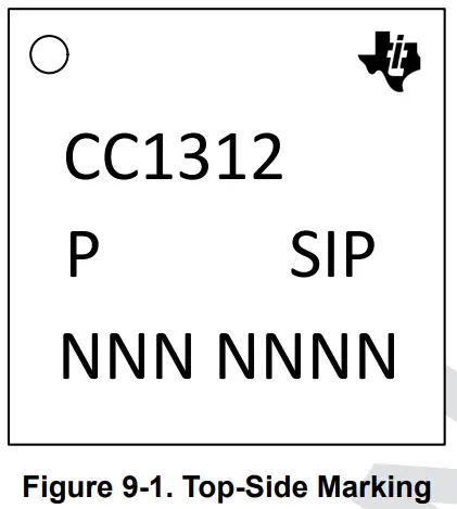
Table 9-4 lists the CC1312PSIP module markings.
Table 9-4. Module Descriptions
| MARKING | DESCRIPTION |
| CC1312 | Generic Part Number |
| P | Model |
| SIP | SIP = Module type, X = pre-release |
| NNN NNNN | LTC (Lot Trace Code) |
9.17 End Product Labeling
The CC1312PSIPMOT module complies with the FCC single modular FCC grant, FCC ID: ZAT-1312PSIP-1.
The host system using this module must display a visible label indicating the following text:
Contains FCC ID: ZAT-1312PSIP-1
The CC1312PSIPMOT module complies with the IC single modular IC grant, IC: 451H-1312PSIP1. The host system using this module must display a visible label indicating the following text:
Contains IC: 451H-1312PSIP1
For more information on end product labeling and a sample label, please see section 4 of the OEM Integrators Guide
9.18 Manual Information to the End User
The OEM integrator must be aware not to provide information to the end user regarding how to install or remove this RF module in the user’s manual of the end product which integrates this module. The end user manual must include all required regulatory information and warnings as shown in this manual.
Application, Implementation, and Layout
Note
Information in the following Applications section is not part of the TI component specification, and TI does not warrant its accuracy or completeness. TI’s customers are responsible for determining suitability of components for their purposes. Customers should validate and test their design implementation to confirm system functionality.
10.1 Application Information
10.1.1 Typical Application Circuit
Figure 10-1 shows the typical application schematic using the CC1312PSIP module. For the full reference schematic, download the LP-EM-CC1312PSIP Design Files.
Note
The following guidelines are recommended for implementation of the RF design:
- Ensure an RF path is designed with a characteristic impedance of 50 Ω.
- Tuning of the antenna impedance matching network is recommended after manufacturing of the PCB to account for PCB parasitics. Please refer to CC13xx/CC26xx Hardware Configuration and PCB Design Considerations; section 5.1 for further information.

Table 10-1 provides the bill of materials for a typical application using the CC1312PSIP module in Figure 10-1.
It is always recommended to insert a pi-filter (Z9, Z10 and Z11) between the RF pad and the antenna / SMA connector. When matching towards an antenna, this will minimize the mismatch losses of the antenna. A low-pass match or high-pass matching network can typically be chosen.
For the CC1312PSIP, it is recommended to use a low-pass antenna match since this will both match the antenna but will also act as a low-pass filter function as well. As can be seen in Figure 10-1, Z10 and Z11 form a low-pass antenna match on the LP-EM-CC1312PSIP that has an integrated PCB antenna.
In the event that no matching components are required for the antenna or direct connection to a SMA, it is recommended to use Z10: 5.6 nH and Z11: 1.8 pF as a low-pass filter.
For full operation reference design, see the LP-EM-CC1312PSIP Design Files.
Table 10-1. Bill of Materials
| QTY | PART REFERENCE | VALUE | MANUFACTURER | PART NUMBER |
DESCRIPTION |
| 1 | C57 | 100pF | Murata | GRM0335C1H101GA01D | Capacitor, Ceramic C0G/NP0, 100pF, 50V, -2%/+2%, -55DEGC/+125DEGC, 0201, SMD |
| 1 | U1 | CC1312PSIP | Texas Instruments | CC1312PSIP | IC, CC1312PSIP, LGA73, SMD |
| 1 | Z10 | 8.2nH | Murata | LQP03TN8N2J02D | Inductor, RF, Chip, Non-magnetic core, 8.2nH, -5%/+5%, 0.25A, -55DEGC/ +125DEGC, 0201, SMD |
| 1 | Z11 | 1.8pF | Murata | GRM0335C1H1R8BA01J | Capacitor, Ceramic C0G/NP0, 1.8pF, 50V, -0.1pF/+0.1pF, -55DEGC/ +125DEGC, 0201, SMD |
10.2 Device Connection and Layout Fundamentals
10.2.1 Reset
In order to meet the module power-on-reset requirements, VDDS (Pin 46) and VDDS_PU (Pin 47) should be connected together. If the reset signal is not based upon a power-on-reset and is instead derived from an external MCU, then VDDS_PU (Pin 47) should be No Connect (NC).
10.2.2 Unused Pins
All unused pins can be left unconnected without the concern of having leakage current. Please refer to #unique_98 for more details.
10.3 PCB Layout Guidelines
This section details the PCB guidelines to speed up the PCB design using the CC1312PSIP module. The integrator of the modules must comply with the PCB layout recommendations described in the following subsections to minimize the risk with regulatory certifications for the FCC, IC/ISED, ETSI/CE. Moreover, TI recommends customers to follow the guidelines described in this section to achieve similar performance to that obtained with the TI reference design.
10.3.1 General Layout Recommendations
Ensure that the following general layout recommendations are followed:
- Have a solid ground plane and ground vias under the module for stable system and thermal dissipation.
- Do not run signal traces underneath the module on a layer where the module is mounted.
10.3.2 RF Layout Recommendations
It is critical that the RF section be laid out correctly to ensure optimal module performance. A poor layout can cause low-output power and sensitivity degradation. Figure 10-2 shows the RF placement and routing of the module with the 2.4-GHz inverted F antenna.
Follow these RF layout recommendations for the module:
- RF traces must have a chararcterisitc impedance of 50-Ω.
- There must be no traces or ground under the antenna section.
- RF traces must have via stitching on the ground plane beside the RF trace on both sides.
- RF traces must be as short as possible.
- The module must be as close to the PCB edge in consideration of the product enclosure and type of antenna being used.
10.3.2.1 Antenna Placement and Routing
The antenna is the element used to convert the guided waves on the PCB traces to the free space electromagnetic radiation. The placement and layout of the antenna are the keys to increased range and data rates. Table 10-2 provides a summary of the antenna guidelines to follow with the CC1312PSIPmodule.
Table 10-2. Antenna Guidelines
| SR NO. | GUIDELINES |
| 1 | Place the antenna on an edge of the PCB. |
| 2 | Ensure that no signals are routed across the antenna elements on any PCB layer. |
| 3 | Most antennas, including the PCB antenna used on the LaunchPad™, require ground clearance on all the layers of the PCB. Ensure that the ground is cleared on inner layers as well. |
| 4 | Ensure that there is provision to place matching components for the antenna. These must be tuned for best return loss when the complete board is assembled. Any plastics or casing must also be mounted while tuning the antenna because this can impact the impedance. |
| 5 | Ensure that the antenna characteristic impedance is 50-Ω as the module is designed for a 50-Ω system. |
| 6 | In case of printed antenna, ensure that the simulation is performed considering the soldermask thickness. |
| 7 | For good RF performance ensrue that the Voltge Standing Wave Ration (VSWR) is less than 2 across the frequency band of interest. |
| 9 | The feed point of the antenna is required to be grounded. This is only for the antenna type used on theLP-EM-CC1312PSIP LaunPad™. See the specific antenna data sheets for the recommendations. |
Table 10-3 lists the recommended antennas to use with the CC1312PSIPmodule. Other antennas may be available for use with the CC1312PSIPmodule. Please refer to to the for a list of approved antennas (and antenna types) that can be used with the CC1312PSIP module.
Table 10-3. Recommended Antennas
| CHOICE | ANTENNA | MANUFACTURER | NOTES |
| 1 | Integrated PCB antenna on the LP-EM- CC1312PSIP | Texas Instruments | +2.7 dBi gain at 915 MHz, see the LP-EM-CC1312PSIP refference design |
| 2 | External whip antenna | Nearson, S463AM-915 | +2.0 dBi gain at 915 MHz, https://www.nearson.com/assets/pdfs/Antenna/S463XX-915.pdf, |
| 3 | External whip antenna | Pulse, W5017 | +0.9 dBi gain at 915 MHz |
| 4 | Chip antenna | Johanson Technology, 0900AT43A0070 | -0.5 dBi gain at 915 MHz |
| 5 | Chip antenna | Johanson Technology, 0915AT43A0026 | +1.4 dBi gain at 915 MHz |
| 6 | Helical wire antenna | Pulse, W3113 | +0.8 dBi gain at 915 MHz |
10.3.2.2 Transmission Line Considerations
The RF signal from the module is routed to the antenna using a Coplanar Waveguide with ground (CPW-G) structure. CPW-G structure offers the maximum amount of isolation and the best possible shielding to the RF lines. In addition to the ground on the L1 layer, placing GND vias along the line also provides additional shielding.
Figure 10-3 shows a cross section of the coplanar waveguide with the critical dimensions.
Figure 10-4 shows the top view of the coplanar waveguide with GND and via stitching.
The recommended values for a 4-layer PCB board is provided in Table 10-4.
Table 10-4. Recommended PCB Values for 4-Layer
Board (L1 to L2 = 0.175 mm)
 10.4 Reference Designs
The following reference designs should be followed closely when implementing designs using the CC1312PSIP device.
Special attention must be paid to RF component placement, decoupling capacitors and DCDC regulator components, as well as ground connections for all of these.
| LP-EM-CC1312PSIP Design Files |
The LP-EM-CC1312PSIP reference design provides schematic, layout and production files for the characterization board used for deriving the performance number found in this document. |
| Sub-1 GHz and 2.4 GHz Antenna Kit for LaunchPad™ Development Kit and SensorTag |
The antenna kit allows real-life testing to identify the optimal antenna for your application. The antenna kit includes 16 antennas for frequencies from 169 MHz to 2.4 GHz, including: • PCB antennas • Helical antennas • Chip antennas • Dual-band antennas for 868 MHz and 915 MHz combined with 2.4 GHz The antenna kit includes a JSC cable to connect to the Wireless MCU LaunchPad Development Kits and SensorTags. |
Environmental Requirements and SMT Specifications
11.1 PCB Bending
The PCB follows IPC-A-600J for PCB twist and warpage < 0.75% or 7.5 mil per inch.
11.2 Handling Environment
11.2.1 Terminals
The product is mounted with motherboard through land-grid array (LGA). To prevent poor soldering, do not make skin contact with the LGA portion.
11.2.2 Falling
The mounted components will be damaged if the product falls or is dropped. Such damage may cause the product to malfunction.
11.3 Storage Condition
11.3.1 Moisture Barrier Bag Before Opened
A moisture barrier bag must be stored in a temperature of less than 30°C with humidity under 85% RH. The calculated shelf life for the dry-packed product will be 24 months from the date the bag is sealed.
11.3.2 Moisture Barrier Bag Open
Humidity indicator cards must be blue, < 30%.
11.4 PCB Assembly Guide
The wireless MCU modules are packaged in a substrate base Leadless Quad Flatpack (QFM) package. The modules are designed with pull back leads for easy PCB layout and board mounting.
11.4.1 PCB Land Pattern & Thermal Vias
We recommended a solder mask defined land pattern to provide a consistent soldering pad dimension in order to obtain better solder balancing and solder joint reliability. PCB land pattern are 1:1 to module soldering pad dimension. Thermal vias on PCB connected to other metal plane are for thermal dissipation purpose. It is critical to have sufficient thermal vias to avoid device thermal shutdown. Recommended vias size are 0.2mm and position not directly under solder paste to avoid solder dripping into the vias.
11.4.2 SMT Assembly Recommendations
The module surface mount assembly operations include:
- Screen printing the solder paste on the PCB
- Monitor the solder paste volume (uniformity)
- Package placement using standard SMT placement equipment
- X-ray pre-reflow check – paste bridging
- Reflow
- X-ray post-reflow check – solder bridging and voids
11.4.3 PCB Surface Finish Requirements
A uniform PCB plating thickness is key for high assembly yield. For an electroless nickel immersion gold finish, the gold thickness should range from 0.05 µm to 0.20 µm to avoid solder joint embrittlement. Using a PCB with Organic Solderability Preservative (OSP) coating finish is also recommended as an alternative to Ni-Au.
11.4.4 Solder Stencil
Solder paste deposition using a stencil-printing process involves the transfer of the solder paste through predefined apertures with the application of pressure. Stencil parameters such as aperture area ratio and the fabrication process have a significant impact on paste deposition. Inspection of the stencil prior to placement of package is highly recommended to improve board assembly yields.
11.4.5 Package Placement
Packages can be placed using standard pick and place equipment with an accuracy of ±0.05 mm. Component pick and place systems are composed of a vision system that recognizes and positions the component and a mechanical system that physically performs the pick and place operation. Two commonly used types of vision systems are:
- A vision system that locates a package silhouette
- A vision system that locates individual pads on the interconnect pattern
The second type renders more accurate placements but tends to be more expensive and time consuming. Both methods are acceptable since the parts align due to a self-centering features of the solder joint during solder reflow. It is recommended to avoid solder bridging to 2 mils into the solder paste or with minimum force to avoid causing any possible damage to the thinner packages.
11.4.6 Solder Joint Inspection
After surface mount assembly, transmission X-ray should be used for sample monitoring of the solder attachment process. This identifies defects such as solder bridging, shorts, opens, and voids. It is also recommended to use side view inspection in addition to X-rays to determine if there are “Hour Glass” shaped solder and package tilting existing. The “Hour Glass” solder shape is not a reliable joint. 90° mirror projection can be used for side view inspection.
11.4.7 Rework and Replacement
TI recommends removal of modules by rework station applying a profile similar to the mounting process. Using a heat gun can sometimes cause damage to the module by overheating.
11.4.8 Solder Joint Voiding
TI recommends to control solder joint voiding to be less than 30% (per IPC-7093). Solder joint voids could be reduced by baking of components and PCB, minimized solder paste exposure duration, and reflow profile optimization.
11.5 Baking Conditions
Products require baking before mounting if:
- Humidity indicator cards read > 30%
- Temp < 30°C, humidity < 70% RH, over 96 hours
Baking condition: 90°C, 12 to 24 hours
Baking times: 1 time
11.6 Soldering and Reflow Condition
- Heating method: Conventional convection or IR convection
- Temperature measurement: Thermocouple d = 0.1 mm to 0.2 mm CA (K) or CC (T) at soldering portion or equivalent method
- Solder paste composition: SAC305
- Allowable reflow soldering times: 2 times based on the reflow soldering profile (see Figure 11-1)
- Temperature profile: Reflow soldering will be done according to the temperature profile (see Figure 11-1)
- Peak temperature: 260°C
 Figure 11-1. Temperature Profile for Evaluation of Solder Heat Resistance of a Component (at Solder Joint)
Table 11-1. Temperature Profile
| Profile Elements | Convection or IR(1) |
| Peak temperature range | 235 to 240°C typical (260°C maximum) |
| Pre-heat / soaking (150 to 200°C) | 60 to 120 seconds |
| Time above melting point | 60 to 90 seconds |
| Time with 5°C to peak | 30 seconds maximum |
| Ramp up | < 3°C / second |
| Ramp down | < -6°C / second |
(1) For details, refer to the solder paste manufacturer’s recommendation.
Note
TI does not recommend the use of conformal coating or similar material on the SimpleLink™ module.
This coating can lead to localized stress on the solder connections inside the module and impact the module reliability. Use caution during the module assembly process to the final PCB to avoid the presence of foreign material inside the module.
Device and Documentation Support
TI offers an extensive line of development tools. Tools and software to evaluate the performance of the device, generate code, and develop solutions are listed as follows.
12.1 Device Nomenclature
To designate the stages in the product development cycle, TI assigns prefixes to all part numbers and/or datecode.
Each device has one of three prefixes/identifications: X, P, or null (no prefix) (for example, XCC1312PSIP is in preview; therefore, an X prefix/identification isassigned).
Device development evolutionary flow:
X Experimental device that is not necessarily representative of the final device’s electrical specifications and may not use production assembly flow.
P Prototype device that is not necessarily the final silicon die and may not necessarily meet final electrical specifications.
null Production version of the silicon die that is fully qualified.
Production devices have been characterized fully, and the quality and reliability of the device have been demonstrated fully. TI’s standard warranty applies.
Predictions show that prototype devices (X or P) have a greater failure rate than the standard production devices. Texas Instruments recommends that these devices not be used in any production system because their expected end-use failure rate still is undefined. Only qualified production devices are to be used.
TI device nomenclature also includes a suffix with the device family name. This suffix indicates the package type (for example, RGZ).
For orderable part numbers of CC1312PSIP devices in the RGZ (7-mm x 7-mm) package type, see the Package Option Addendum of this document, the Device Information in Section 3, the TI website (www.ti.com), or contact your TI sales representative.
12.2 Tools and Software
The CC1312PSIP device is supported by a variety of software and hardware development tools.
Development Kit
Software
| SimpleLink™ CC13xx and CC26xx Software | The SimpleLink CC13xx-CC26xx Software Development Kit (SDK) provides a complete package for the development of wireless applications on the CC13x2 / CC26x2 family |
| Development Kit (SDK) | of devices. The SDK includes a comprehensive software package for the CC1312PSIP device, including the following protocol stacks: • Wi-SUN® • TI 15.4-Stack – an IEEE 802.15.4-based star networking solution for Sub-1 GHz and 2.4 GHz • Prop RF API – a flexible set of building blocks for developing proprietary RF software stacks The SimpleLink CC13xx-CC26xx SDK is part of TI’s SimpleLink MCU platform, offering a single development environment that delivers flexible hardware, software and tool options for customers developing wired and wireless applications. For more information about the SimpleLink MCU Platform, visit https://www.ti.com/simplelink. |
Development Tools
| Code Composer Studio™ Integrated Development Environment (IDE) | Code Composer Studio is an integrated development environment (IDE) that supports TI’s Microcontroller and Embedded Processors portfolio. Code Composer Studio comprises a suite of tools used to develop and debug embedded applications. It includes an optimizing C/C++ compiler, source code editor, project build environment, debugger, profiler, and many other features. The intuitive IDE provides a single user interface taking you through each step of the application development flow. Familiar tools and interfaces allow users to get started faster than ever before. Code Composer Studio combines the advantages of the Eclipse® software framework with advanced embedded debug capabilities from TI resulting in a compelling feature-rich development environment for embedded developers. CCS has support for all SimpleLink Wireless MCUs and includes support for EnergyTrace™ software (application energy usage profiling). A real-time object viewer plugin is available for TI-RTOS, part of the SimpleLink SDK. Code Composer Studio is provided free of charge when used in conjunction with the XDS debuggers included on a LaunchPad Development Kit. |
| Code Composer Studio™ Cloud IDE | Code Composer Studio (CCS) Cloud is a web-based IDE that allows you to create, edit and build CCS and Energia™ projects. After you have successfully built your project, you can download and run on your connected LaunchPad. Basic debugging, including features like setting breakpoints and viewing variable values is now supported with CCS Cloud. |
| IAR Embedded Workbench® for Arm® | IAR Embedded Workbench® is a set of development tools for building and debugging embedded system applications using assembler, C and C++. It provides a completely integrated development environment that includes a project manager, editor, and build tools. IAR has support for all SimpleLink Wireless MCUs. It offers broad debugger support, including XDS110, IAR I-jet™ and Segger J-Link™. A real-time object viewer plugin is available for TI-RTOS, part of the SimpleLink SDK. IAR is also supported out-of-the-box on most software examples provided as part of the SimpleLink SDK. A 30-day evaluation or a 32 KB size-limited version is available through iar.com. |
| SmartRF™ Studio | SmartRF™ Studio is a Windows® application that can be used to evaluate and configure SimpleLink Wireless MCUs from Texas Instruments. The application will help designers of RF systems to easily evaluate the radio at an early stage in the design process. It is especially useful for generation of configuration register values and for practical testing and debugging of the RF system. SmartRF Studio can be used either as a standalone application or together with applicable evaluation boards or debug probes for the RF device. Features of the SmartRF Studio include:
• Link tests – send and receive packets between nodes |
12.2.1 SimpleLink™ Microcontroller Platform
The SimpleLink microcontroller platform sets a new standard for developers with the broadest portfolio of wired and wireless Arm
MCUs (System-on-Chip) in a single software development environment. Delivering flexible hardware, software and tool options for your IoT applications. Invest once in the SimpleLink software development kit and use throughout your entire portfolio. Learn more on ti.com/simplelink.
12.3 Documentation Support
To receive notification of documentation updates on data sheets, errata, application notes and similar, navigate to the device product folder on ti.com/product/CC1312PSIP. In the upper right corner, click on Alert me to register and receive a weekly digest of any product information that has changed. For change details, review the revision history included in any revised document.
The current documentation that describes the MCU, related peripherals, and other technical collateral is listed as follows.
TI Resource Explorer
TI Resource Explorer
Software examples, libraries, executables, and documentation are available for your device and development board.
Errata
CC1312PSIP Silicon Errata
The silicon errata describes the known exceptions to the functional specifications for each silicon revision of the device and description on how to recognize a device revision.
Application Reports
All application reports for the CC1312PSIP device are found on the device product folder at: ti.com/product/CC1312PSIP/technicaldocuments.
Technical Reference Manual (TRM)
CC13x2, CC26x2 SimpleLink™ Wireless MCU TRM
The TRM provides a detailed description of all modules and peripherals available in the device family.
12.4 Support Resources
support forums are an engineer’s go-to source for fast, verified answers and design help — straight from the experts. Search existing answers or ask your own question to get the quick design help you need. ™ Linked content is provided AS IS” by the respective contributors. They do not constitute TI specifications and do not necessarily reflect TI’s views; see TI’s Terms of Use. 12.5 Trademarks are trademarks of Texas Instruments. I-jet SimpleLink ™ , LaunchPad ™ , Code Composer Studio ™ , EnergyTrace ™ , and TI E2E ™ is a trademark of IAR Systems AB. J-Link ™ is a trademark of SEGGER Microcontroller Systeme GmbH. Arm ™ are registered trademarks of Arm Limited (or its subsidiaries) n the US and/or elsewhere. CoreMark ® and Cortex ® tr ictio n s is a registered trademark of Embedded Microprocessor Benchmark Consortium Corporation. Arm Thumb ® is a registered trademark of Arm Limited (or its subsidiaries). Eclipse ® is a registered trademark of Eclipse Foundation. IAR Embedded Workbench ® is a registered trademark of IAR Systems AB. Windows ® is a registered trademark of Microsoft Corporation. All trademarks are the property of their respective owners. ®
12.6 Electrostatic Discharge Caution
12.6 Electrostatic Discharge Caution
This integrated circuit can be damaged by ESD. Texas Instruments recommends that all integrated circuits be handled with appropriate precautions. Failure to observe proper handling and installation procedures can cause damage.
ESD damage can range from subtle performance degradation to complete device failure. Precision integrated circuits may be more susceptible to damage because very small parametric changes could cause the device not to meet its published specifications.
12.7 Glossary
TI Glossary
This glossary lists and explains terms, acronyms, and definitions.
Mechanical, Packaging, and Orderable Information
The following pages include mechanical packaging and orderable information. This information is the most current data available for the designated devices. This data is subject to change without notice and revision of this document. For browser-based versions of this data sheet, refer to the left-hand navigation.
Note
The total height of the module is 1.51 mm.
The weight of the CC1312PSIP module is typically 0.19 g.
NOTES:
- All linear dimensions are in millimeters. Any dimensions in parenthesis are for reference only. Dimensioning and tolerancing per ASME Y14.5M.
- This drawing is subject to change without notice.
EXAMPLE BOARD LAYOUT QFM – 1.51 mm max height
MOT0048A
- This package is designed to be soldered to a thermal pad on the board. For more information, see Texas Instruments literature number SLUA271 (www.ti.com/lit/slua271).

- Laser cutting apertures with trapezoidal walls and rounded corners may offer better paste release. IPC-7525 may have alternate design recommendations.
IMPORTANT NOTICE AND DISCLAIMER
TI PROVIDES TECHNICAL AND RELIABILITY DATA (INCLUDING DATA SHEETS), DESIGN RESOURCES (INCLUDING REFERENCE DESIGNS), APPLICATION OR OTHER DESIGN ADVICE, WEB TOOLS, SAFETY INFORMATION, AND OTHER RESOURCES “AS IS” AND WITH ALL FAULTS, AND DISCLAIMS ALL WARRANTIES, EXPRESS AND IMPLIED, INCLUDING WITHOUT LIMITATION ANY IMPLIED WARRANTIES OF MERCHANTABILITY, FITNESS FOR A PARTICULAR PURPOSE OR NON-INFRINGEMENT OF THIRD PARTY INTELLECTUAL PROPERTY RIGHTS.
These resources are intended for skilled developers designing with TI products. You are solely responsible for (1) selecting the appropriate TI products for your application, (2) designing, validating and testing your application, and (3) ensuring your application meets applicable standards, and any other safety, security, regulatory or other requirements.
These resources are subject to change without notice. TI grants you permission to use these resources only for development of an application that uses the TI products described in the resource. Other reproduction and display of these resources is prohibited. No license is granted to any other TI intellectual property right or to any third party intellectual property right. TI disclaims responsibility for, and you will fully indemnify TI and its representatives against, any claims, damages, costs, losses, and liabilities arising out of your use of these resources.
TI’s products are provided subject to TI’s Terms of Sale or other applicable terms available either on ti.com or provided in conjunction with such TI products. TI’s provision of these resources does not expand or otherwise alter TI’s applicable warranties or warranty disclaimers for TI products.
TI objects to and rejects any additional or different terms you may have proposed.
IMPORTANT NOTICE Mailing Address: Texas Instruments, Post Office Box 655303, Dallas, Texas 75265
Copyright © 2023, Texas Instruments Incorporated
Copyright © 2023 Texas Instruments Incorporated
Product Folder Links: CC1312PSIP
Submit Document Feedback
www.ti.com
Documents / Resources
 |
TEXAS INSTRUMENTS CC1312PSIP SimpleLink Sub-1-GHz Wireless System-in-Package [pdf] Owner's Manual CC1312PSIP SimpleLink Sub-1-GHz Wireless System-in-Package, CC1312PSIP, SimpleLink Sub-1-GHz Wireless System-in-Package, Sub-1-GHz Wireless System-in-Package, Wireless System-in-Package, System-in-Package |