intel F-Tile CPRI PHY FPGA IP Design Example

Dali nga Giya sa Pagsugod
Ang F-Tile CPRI PHY Intel® FPGA IP core naghatag ug simulation testbench ug hardware design example nga nagsuporta sa compilation ug hardware testing. Kung makamugna ka sa disenyo exampUg, ang editor sa parameter awtomatikong nagmugna sa files gikinahanglan sa simulate, compile, ug pagsulay sa disenyo sa hardware.
Naghatag usab ang Intel og compilation-only exampAng proyekto nga imong magamit aron dali nga mabanabana ang IP core area ug timing.
Ang F-Tile CPRI PHY Intel FPGA IP core naghatag sa kapabilidad sa pagmugna og disenyo examples alang sa tanang suportadong kombinasyon sa gidaghanon sa CPRI channels ug CPRI line bit rates. Ang testbench ug disenyo exampGisuportahan ang daghang mga kombinasyon sa parameter sa F-Tile CPRI PHY Intel FPGA IP core.
Figure 1. Mga Lakang sa Pag-uswag alang sa Disenyo Example

May Kalabutan nga Impormasyon
- F-Tile CPRI PHY Intel FPGA IP User Guide
- Para sa detalyadong impormasyon sa F-tile CPRI PHY IP.
- F-Tile CPRI PHY Intel FPGA IP Release Notes
- Ang IP Release Notes naglista sa mga pagbag-o sa IP sa usa ka partikular nga pagpagawas.
Mga Kinahanglanon sa Hardware ug Software
Para testingan ang exampsa disenyo, gamita ang mosunod nga hardware ug software:
- Intel Quartus® Prime Pro Edition software
- Sistema nga console
- Gisuportahan nga mga Simulator:
- Mga Synopsy* VCS*
- Synopsys VCS MX
- Siemens* EDA ModelSim* SE o Questa*— Questa-Intel FPGA Edition
Paghimo sa Disenyo
Hulagway 2. Pamaagi
 Hulagway 3. Example Design Tab sa IP Parameter Editor

Aron makahimo usa ka proyekto sa Intel Quartus Prime Pro Edition:
- Sa Intel Quartus Prime Pro Edition, i-klik File ➤ Bag-ong Project Wizard aron makahimo og bag-ong proyekto sa Quartus Prime, o File ➤ Buksan ang Proyekto aron maablihan ang kasamtangan nga proyekto sa Intel Quartus Prime. Ang wizard nag-aghat kanimo sa pagtino sa usa ka aparato.
- Ipiho ang pamilya sa device nga Agilex (I-series) ug pagpili og device nga makatuman sa tanan niini nga mga kinahanglanon:
- Ang transceiver tile kay F-tile
- Ang grado sa gikusgon sa transceiver kay -1 o -2
- Ang grado sa core speed kay -1 o -2 o -3
- I-klik ang Tapos.
Sunda kini nga mga lakang aron makamugna ang F-Tile CPRI PHY Intel FPGA IP hardware design example ug testbench:
- Sa IP Catalog, pangitaa ug pilia ang F-Tile CPRI PHY Intel FPGA IP. Ang Bag-ong IP Variation nga bintana makita.
- Itakda ang usa ka top-level nga ngalan para sa imong custom IP variation. Gitipigan sa editor sa parameter ang mga setting sa pagbag-o sa IP sa a file ginganlan .ip.
- I-klik ang OK. Ang parameter editor makita.
- Sa tab nga IP, ipiho ang mga parameter alang sa imong IP core variation.
- Sa Example Design tab, ubos sa Example Disenyo Files, pilia ang opsyon sa Simulation aron makamugna ang testbench ug ang compilation-only nga proyekto. Pilia ang opsyon sa Synthesis aron makamugna ang disenyo sa hardware example. Kinahanglan ka nga mopili bisan usa sa mga kapilian sa Simulation ug Synthesis aron makamugna ang disenyo nga example.
- Sa Example Design tab, ubos sa Generated HDL Format, pilia ang Verilog HDL o VHDL. Kung imong pilion ang VHDL, kinahanglan nimo nga i-simulate ang testbench gamit ang usa ka mixed-language simulator. Ang aparato nga gisulayan sa ex_ direktoryo mao ang usa ka VHDL modelo, apan ang nag-unang testbench file mao ang System Verilog file.
- I-klik ang Generate Exampang buton sa Disenyo. Ang Pagpili ExampAng bintana sa Direktoryo sa Disenyo makita.
- Kung gusto nimo usbon ang disenyo example direktoryo nga agianan o ngalan gikan sa mga default nga gipakita (cpriphy_ftile_0_example_design), browse sa bag-ong dalan ug i-type ang bag-ong disenyo exampngalan sa direktoryo (ample_dir>).
Istruktura sa Direktoryo
Ang F-Tile CPRI PHY Intel FPGA IP core design example file ang mga direktoryo naglangkob sa mosunod nga namugna files alang sa disenyo example.
Figure 4. Direktoryo Structure sa Namugna Example Disenyo

Talaan 1. Testbench File Mga paghulagway
| File Mga ngalan | Deskripsyon |
| Key Testbench ug Simulation Files | |
| <design_example_dir>/ example_testbench/basic_avl_tb_top.sv | Top-level nga testbench file. Gi-instantiate sa testbench ang DUT wrapper ug gipadagan ang mga buluhaton sa Verilog HDL aron makamugna ug makadawat mga pakete. |
| <design_example_dir>/ example_testbench/ cpriphy_ftile_wrapper.sv | DUT wrapper nga instantiates DUT ug uban pang testbench nga mga sangkap. |
| Testbench Scripts(1) | |
| <design_example_dir>/ example_testbench/run_vsim.do | Ang Siemens EDA ModelSim SE o Questa o Questa-Intel FPGA Edition nga script aron ipadagan ang testbench. |
| <design_example_dir>/ example_testbench/run_vcs.sh | Ang script sa Synopsys VCS aron mapadagan ang testbench. |
| <design_example_dir>/ example_testbench/run_vcsmx.sh | Ang Synopsys VCS MX script (kombinar Verilog HDL ug SystemVerilog uban sa VHDL) aron modagan ang testbench. |
Ibaliwala ang bisan unsang ubang script sa simulator saample_dir>/example_testbench/ folder.
Talaan 2. Disenyo sa Hardware Example File Mga paghulagway
| File Mga ngalan | Mga paghulagway |
| <design_example_dir>/hardware_test_design/ cpriphy_ftile_hw.qpf | Intel Quartus Prime nga proyekto file. |
| <design_example_dir>/hardware_test_design/ cpriphy_ftile_hw.qsf | Setting sa proyekto sa Intel Quartus Prime file. |
| <design_example_dir>/hardware_test_design/ cpriphy_ftile_hw.sdc | Mga Limitasyon sa Disenyo sa Synopsy files. Mahimo nimong kopyahon ug usbon kini filealang sa imong kaugalingong Intel Agilex™ nga disenyo. |
| <design_example_dir>/hardware_test_design/ cpriphy_ftile_hw.v | Top-level nga Verilog HDL nga disenyo example file. |
| <design_example_dir>/hardware_test_design/ cpriphy_ftile_wrapper.sv | DUT wrapper nga instantiates DUT ug uban pang testbench nga mga sangkap. |
| <design_example_dir>/hardware_test_design/ hwtest_sl/main_script.tcl | Panguna file alang sa pag-access sa System Console. |
Pagsundog sa Disenyo Exampsa Testbench
Hulagway 5. Pamaagi

Sunda kini nga mga lakang aron ma-simulate ang testbench:
- Sa command prompt, usba ang direktoryo sa simulation sa testbenchample_dir>/example_testbench. cd /example_testbench
- Pagdalagan ang quartus_tlg sa namugna nga proyekto file: quartus_tlg cpriphy_ftile_hw
- Pagdalagan ip-setup-simulation: ip-setup-simulation –output-directory=./sim_script –use-relative-paths –quartus project=cpriphy_ftile_hw.qpf
- Pagdalagan ang simulation script para sa gisuportahan nga simulator nga imong gusto. Ang script nag-compile ug nagpadagan sa testbench sa simulator. Tan-awa ang lamesa Mga Lakang sa Pag-simulate sa Testbench.
- Analisaha ang mga resulta. Ang malampuson nga testbench nakadawat og lima ka hyperframes, ug nagpakita sa "PASED".
Talaan 3. Mga Lakang sa Pag-simulate sa Testbench sa Synopsys VCS* Simulator
| Simulator | Mga instruksyon | |
| VCS | Sa command line, i-type ang: | |
| sh run_vcs.sh | ||
| nagpadayon… | ||
| Simulator | Mga instruksyon | |
| VCS MX | Sa command line, i-type ang: | |
| sh run_vcsmx.sh | ||
| ModelSim SE o Questa o Questa-Intel FPGA Edition | Sa command line, i-type ang: | |
| vsim -do run_vsim.do | ||
| Kung gusto nimo nga mag-simulate nga wala magdala sa GUI, i-type ang: | ||
| vsim -c -do run_vsim.do | ||
Ang mosunod nga sampAng output naghulagway sa usa ka malampuson nga simulation test run alang sa 24.33024 Gbps nga adunay 4 ka CPRI channels:


Pag-compile sa Compilation-Only Project
Sa pag-compile sa compilation-only exampsa proyekto, sunda kini nga mga lakang:
- Siguradoha ang disenyo sa compilation exampkompleto na ang henerasyon.
- Sa software nga Intel Quartus Prime Pro Edition, ablihi ang proyekto sa Intel Quartus Prime Pro Editionample_dir>/compilation_test_design/cpriphy_ftile.qpf.
- Sa Processing menu, i-klik ang Start Compilation.
- Human sa malampuson nga paghugpong, ang mga taho alang sa tayming ug alang sa paggamit sa kahinguhaan anaa sa imong sesyon sa Intel Quartus Prime Pro Edition.
May Kalabutan nga Impormasyon
Mga Agos sa Disenyo nga Gibase sa Block
Pag-compile ug Pag-configure sa Disenyo Exampsa Hardware
Sa pag-compile sa hardware design exampug i-configure kini sa imong Intel Agilex device, sunda kini nga mga lakang:
- Siguroha ang disenyo sa hardware exampkompleto na ang henerasyon.
- Sa Intel Quartus Prime Pro Edition software, ablihi ang Intel Quartus Prime nga proyektoample_dir>/hardware_test_design/ cpriphy_ftile_hw.qpf.
- I-edit ang .qsf file sa paghatag ug mga pin base sa imong hardware.
- Sa Processing menu, i-klik ang Start Compilation.
- Human sa malampuson nga paghugpong, usa ka .sof file anaa saample_dir>/hardware_test_design/output_files direktoryo.
Sunda kini nga mga lakang sa programa sa hardware design exampsa Intel Agilex device:
- Ikonektar ang Intel Agilex I-series Transceiver Signal Integrity Development Kit sa host computer.
Mubo nga sulat: Ang development kit giprograma nang daan gamit ang hustong frequency sa orasan pinaagi sa default. Dili nimo kinahanglan nga gamiton ang aplikasyon sa Clock Control aron itakda ang mga frequency. - Sa Tools menu, i-klik ang Programmer.
- Sa Programmer, i-klik ang Hardware Setup.
- Pagpili ug programming device.
- Siguroha nga ang Mode gitakda sa JTAG.
- Pilia ang Intel Agilex device ug i-klik ang Add Device. Ang Programmer nagpakita og block diagram sa mga koneksyon tali sa mga device sa imong board.
- Sa laray sa imong .sof, susiha ang kahon alang sa .sof.
- I-tsek ang kahon sa Program/Configure column.
- I-klik ang Start.
May Kalabutan nga Impormasyon
- Mga Agos sa Disenyo nga Gibase sa Block
- Pagprograma sa Intel FPGA Devices
- Pag-analisar ug Pag-debug sa mga Disenyo gamit ang System Console
Pagsulay sa Hardware Design Example
Human nimo makolekta ang F-Tile CPRI PHY Intel FPGA IP core design exampug i-configure kini sa imong Intel Agilex device, mahimo nimong gamiton ang System Console aron maprograma ang IP core ug ang PHY IP core registers niini.
Aron ma-on ang System Console ug sulayan ang disenyo sa hardware example, sunda kini nga mga lakang:
- Pagkahuman sa disenyo sa hardware example gi-configure sa Intel Agilex device, sa Intel Quartus Prime Pro Edition software, sa Tools menu, i-klik ang System Debugging Tools ➤ System Console.
- Sa Tcl Console pane, i-type ang cd hwtest aron usbon ang direktoryo saample_dir>/hardware_test_design/hwtest_sl.
- Type source main_script.tcl aron maablihan ang koneksyon sa JTAG master ug sugdi ang pagsulay.
Disenyo Exampang Deskripsyon
Ang disenyo exampGipakita sa le ang batakang pagpaandar sa F-Tile CPRI PHY Intel FPGA IP core. Mahimo nimong makamugna ang disenyo gikan sa Example Design tab sa F-Tile CPRI PHY Intel FPGA IP parameter editor.
Aron makamugna ang disenyo exampUg, kinahanglan nimo nga una nga itakda ang mga kantidad sa parameter alang sa pagbag-o sa IP core nga gusto nimo nga himuon sa imong katapusan nga produkto. Mahimo nimong pilion ang paghimo sa disenyo nga example adunay o wala ang RS-FEC nga bahin. Ang RS-FEC nga bahin anaa sa 10.1376, 12.1651 ug 24.33024 Gbps CPRI line bit rates.
Talaan 4. F-Tile CPRI PHY Intel FPGA IP Core Feature Matrix
| CPRI Line Bit Rate (Gbps) | Suporta sa RS-FEC | Reperensya nga Orasan (MHz) | Deterministic Latency nga Suporta |
| 1.2288 | Dili | 153.6 | Oo |
| 2.4576 | Dili | 153.6 | Oo |
| 3.072 | Dili | 153.6 | Oo |
| 4.9152 | Dili | 153.6 | Oo |
| 6.144 | Dili | 153.6 | Oo |
| 9.8304 | Dili | 153.6 | Oo |
| 10.1376 | Uban ug Wala | 184.32 | Oo |
| 12.1651 | Uban ug Wala | 184.32 | Oo |
| 24.33024 | Uban ug Wala | 184.32 | Oo |
Mga bahin
- Paghimo sa disenyo example nga adunay bahin sa RS-FEC
- Ang sukaranan nga mga kapabilidad sa pagsusi sa pakete lakip ang pag-ihap sa pag-ikot sa latency
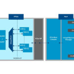
Disenyo sa Simulation Example
Ang F-Tile CPRI PHY Intel FPGA IP design example makamugna og usa ka simulation testbench ug simulation files nga nag-instantiate sa F-Tile CPRI PHY Intel FPGA IP core kung imong pilion ang opsyon sa Simulation.
Figure 6. Block Diagram para sa 10.1316, 12.1651, ug 24.33024 Gbps (uban ug walay RS-FEC) Line Rates
 Figure 7. Block Diagram para sa 1.228, 2.4576, 3.072, 4.9152, 6.144, ug 9.8304 Gbps Line Rate

Niini nga disenyo exampSa pagkakaron, ang simulation testbench naghatag ug batakang kagamitan sama sa pagsugod ug paghulat sa lock, pagpadala ug pagdawat sa mga pakete.
Ang malampuson nga pagsulay run nagpakita sa output nga nagpamatuod sa mosunod nga kinaiya:
- Ang lohika sa kliyente nag-reset sa IP core.
- Ang lohika sa kliyente naghulat alang sa pag-align sa RX datapath.
- Ang lohika sa kliyente nagpadala sa mga hyperframe sa interface sa TX MII ug naghulat sa lima ka mga hyperframe nga madawat sa interface sa RX MII. Ang mga hyperframes gipasa ug nadawat sa MII interface sumala sa CPRI v7.0 specifications.
Mubo nga sulat: Ang mga disenyo sa CPRI nga nagtarget sa 1.2, 2.4, 3, 4.9, 6.1, ug 9.8 Gbps line rate naggamit sa 8b/10b interface ug ang mga disenyo nga nagtarget sa 10.1, 12.1 ug 24.3 Gbps (nga adunay ug walay RS-FEC) naggamit sa MII interface. Kini nga disenyo example naglakip sa usa ka round trip counter sa pag-ihap sa round trip latency gikan sa TX ngadto sa RX. - Ang lohika sa kliyente nagbasa sa round trip latency value ug nagsusi sa sulod ug sa tukma sa hyperframes data sa RX MII nga bahin sa higayon nga makompleto sa counter ang round trip latency count.
May Kalabutan nga Impormasyon
- Mga Detalye sa CPRI
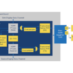
Disenyo sa Hardware Example
Hulagway 8. Disenyo sa Hardware Exampug Block Diagram

Nota
- Ang mga disenyo sa CPRI nga adunay 2.4/4.9/9.8 Gbps nga CPRI line rates naggamit sa 8b/10b interface ug ang tanang ubang CPRI line rates nga mga disenyo naggamit sa MII interface.
- Ang mga disenyo sa CPRI nga adunay 2.4/4.9/9.8 Gbps nga CPRI line rates nagkinahanglan ug 153.6 MHz transceiver reference clock ug ang tanang uban pang CPRI line rates nagkinahanglan ug 184.32 MHz.
Ang F-Tile CPRI PHY Intel FPGA IP core hardware design example naglakip sa mosunod nga mga sangkap:
- F-Tile CPRI PHY Intel FPGA IP core.
- Packet client logic block nga nagmugna ug nakadawat sa trapiko.
- Round trip counter.
- IOPLL aron makamugna sampling clock alang sa deterministic latency logic sulod sa IP, ug round trip counter component sa testbench.
- System PLL aron makamugna og mga orasan sa sistema alang sa IP.
- Avalon®-MM address decoder aron ma-decode ang reconfiguration address space para sa CPRI, Transceiver, ug Ethernet modules atol sa reconfiguration access.
- Mga gigikanan ug mga pagsusi alang sa pagpahayag sa mga pag-reset ug pag-monitor sa mga orasan ug pipila ka mga bit sa status.
- JTAG controller nga nakigsulti sa System Console. Nakigkomunikar ka sa lohika sa kliyente pinaagi sa System Console.
Mga Signal sa Interface
Talaan 5. Disenyo ExampMga Signal sa Interface
| Signal | Direksyon | Deskripsyon |
| ref_clk100MHz | Input | Pag-input nga orasan alang sa pag-access sa CSR sa tanan nga mga interface sa reconfiguration. Pagmaneho sa 100 MHz. |
| i_clk_ref[0] | Input | Reference clock para sa System PLL. Pagmaneho sa 156.25 MHz. |
| i_clk_ref[1] | Input | Reperensya nga orasan sa Transceiver. Pagdrayb sa
• 153.6 MHz para sa CPRI line rate 1.2, 2.4, 3, 4.9, 6.1, ug 9.8 Gbps. • 184.32 MHz alang sa CPRI line rates 10.1,12.1, ug 24.3 Gbps nga adunay ug walay RS-FEC. |
| i_rx_serial[n] | Input | Transceiver PHY input serial data. |
| o_tx_serial[n] | Output | Transceiver PHY output serial data. |
Disenyo Exampmga Register
Talaan 6. Disenyo Exampmga Register
| Numero sa Channel | Base Address (Byte Address) | Uri sa Pagparehistro |
|
0 |
0x00000000 | Ang CPRI PHY Reconfiguration nagparehistro para sa Channel 0 |
| 0x00100000 | Ang Ethernet Reconfiguration nagparehistro para sa Channel 0 | |
| 0x00200000 | Ang Transceiver Reconfiguration nagparehistro para sa Channel 0 | |
|
1(2) |
0x01000000 | Ang CPRI PHY Reconfiguration nagparehistro para sa Channel 1 |
| 0x01100000 | Ang Ethernet Reconfiguration nagparehistro para sa Channel 1 | |
| 0x01200000 | Ang Transceiver Reconfiguration nagparehistro para sa Channel 1 | |
|
2(2) |
0x02000000 | Ang CPRI PHY Reconfiguration nagparehistro para sa Channel 2 |
| 0x02100000 | Ang Ethernet Reconfiguration nagparehistro para sa Channel 2 | |
| 0x02200000 | Ang Transceiver Reconfiguration nagparehistro para sa Channel 2 | |
| nagpadayon… | ||
| Numero sa Channel | Base Address (Byte Address) | Uri sa Pagparehistro |
|
3(2) |
0x03000000 | Ang CPRI PHY Reconfiguration nagparehistro para sa Channel 3 |
| 0x03100000 | Ang Ethernet Reconfiguration nagparehistro para sa Channel 3 | |
| 0x03200000 | Ang Transceiver Reconfiguration nagparehistro para sa Channel 3 |
Kini nga mga rehistro gireserba kung ang channel wala gigamit.
F-Tile CPRI PHY Intel FPGA IP Design Example User Guide Archives
Kung ang usa ka IP core nga bersyon wala gilista, ang giya sa gumagamit alang sa miaging IP core nga bersyon magamit.
| Intel Quartus Prime nga Bersyon | IP Core nga Bersyon | Giya sa Gumagamit |
| 21.2 | 2.0.0 | F-Tile CPRI PHY Intel FPGA IP Design Example Giya sa Gumagamit |
Kasaysayan sa Pagbag-o sa Dokumento para sa F-Tile CPRI PHY Intel FPGA IP Design Example Giya sa Gumagamit
| Bersyon sa Dokumento | Intel Quartus Prime nga Bersyon | Bersyon sa IP | Mga kausaban |
| 2021.10.04 | 21.3 | 3.0.0 |
|
| 2021.06.21 | 21.2 | 2.0.0 | Inisyal nga pagpagawas. |
Intel Corporation. Tanang katungod gigahin. Ang Intel, ang logo sa Intel, ug uban pang mga marka sa Intel mao ang mga marka sa pamatigayon sa Intel Corporation o mga subsidiary niini. Gigarantiya sa Intel ang paghimo sa iyang mga produkto nga FPGA ug semiconductor sa kasamtangang mga espesipikasyon subay sa standard warranty sa Intel, apan adunay katungod sa paghimog mga pagbag-o sa bisan unsang produkto ug serbisyo bisan unsang orasa nga wala’y pahibalo. Ang Intel walay responsibilidad o tulubagon nga naggikan sa aplikasyon o paggamit sa bisan unsang impormasyon, produkto, o serbisyo nga gihulagway dinhi gawas sa dayag nga giuyonan sa pagsulat sa Intel. Gitambagan ang mga kostumer sa Intel nga makuha ang pinakabag-o nga bersyon sa mga detalye sa aparato sa dili pa magsalig sa bisan unsang gipatik nga kasayuran ug sa dili pa magbutang mga order alang sa mga produkto o serbisyo.
*Ang ubang mga ngalan ug mga tatak mahimong maangkon nga gipanag-iya sa uban.
Mga Dokumento / Mga Kapanguhaan
 |
intel F-Tile CPRI PHY FPGA IP Design Example [pdf] Giya sa Gumagamit F-Tile CPRI PHY FPGA IP Design Example, PHY FPGA IP Design Example, F-Tile CPRI IP Design Example, IP Design Exampug, IP Design |