![]()
DEMO MANUAL
DC2784B-A
LTM4700
High Current, PolyPhase® Step-Down
Power µModule Supply with Digital Power
System Management 2 × LTM4700, 200A
DESCRIPTION
Demonstration circuit 2784B-A is a high efficiency, high density, µModule® regulator with 4.5V to 16V input range. The output voltage is adjustable from 0.5V to 1.8V and it can supply 200A maximum load current. The demo board has two LTM®4700 µModule regulators, which is a dual 50A or single 100A step-down regulator with digital power system management. See LTM4700 data sheet for more detailed information.
The DC2784B-A powers up to default settings and produces power based on configuration resistors without the need for any serial bus communication. This allows easy evaluation of the DC/DC converter. To fully explore the extensive power system management features of the part, download the graphical user interface (GUI) software LTpowerPlay® onto your PC and use Analog Devices I²C/SMBus/PMBus dongle DC1613A to connect to the board. The LTpowerPlay allows the user to reconfigure the part on-the-fly and store the configuration in EEPROM, view telemetry of voltage, current, temperature, and fault status.
GUI Download
The software can be downloaded from LTpowerPlay.
For more details and instructions of LTpowerPlay, please refer to LTpowerPlay GUI for LTM4700 Quick Start Guide.
Design files for this circuit board are available.
All registered trademarks and trademarks are the property of their respective owners.
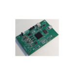
BOARD PHOTO
Part marking is either ink mark or laser mark

Figure 1. 2 × LTM4700; 200A DC2784B-A Demo Circuit
PERFORMANCE SUMMARY
Specifications are at TA = 25°C
| PARAMETER | CONDITIONS | MIN | TYP | MAX | VALUE |
| Input Voltage Range | 4.5 | 16 | V | ||
| Output Voltage, VOUT | VIN = 4.5V to 16V, IOUT = 0A to 200A | 0.5 | 1.0 | 1.8 | V |
| Maximum Output Current, IOUT | VIN = 4.5V to 16V, VOUT = 0.5V to 1.8V | 200 | A | ||
| Typical Efficiency | VIN = 12V, VOUT = 1.0V, IOUT = 200A | 88.7 (See Figure 5) | % | ||
| Default Switching Frequency | 350 | kHz | |||
QUICK START PROCEDURE
Table 1. LTM4700 Demo Boards for Up to 400A Point-of-Load Regulation
| MAXIMUM OUTPUT CURRENT | NUMBER OF OUTPUTS | NUMBER OF LTM4700 µModule REGULATORS ON THE BOARD | DEMO BOARD NUMBER |
| 50A | 2 | 1 | DC2702A-A |
| 100A | 1 | 1 | DC2702A-B |
| 200A | 1 | 2 | DC2784B-A |
| 300A | 1 | 3 | DC2784B-B |
| 400A | 1 | 4 | DC2784B-C |
Demonstration circuit 2784B-A is easy to set up to evaluate the performance of the LTM4700EY. Refer to Figure 2 for the proper measurement equipment setup and follow the procedure below.
- With power off, connect the input power supply to VIN (4.5V to 16V) and GND (input return).
- Connect the 1.0V output load between VOUT and GND (initial load: no load).
- Connect the DVMs to the input and outputs. Set default jumper position: JP1: ON; JP2: ON; JP3: ON.
- Turn on the input power supply and check for the proper output voltages. VOUT should be 1.0V ±0.5%.
- Once the proper output voltages are established, adjust the loads within the operating range and observe the output voltage regulation, ripple voltage and other parameters.
- Connect the dongle and control the output voltages from the GUI. See “LTpowerPlay GUI for the LTM4700 Quick Start Guide” for details.
NOTE: Internal bias circuit is enabled when VIN > 7V and JP3 is ON.
NOTE: When measuring the output or input voltage ripple, do not use the long ground lead on the oscilloscope probe. See Figure 3 for the proper scope probe technique. Short, stiff leads need to be soldered to the (+) and (–) terminals of an output capacitor. The probe’s ground ring needs to touch the (–) lead and the probe tip needs to touch the (+) lead.

DC2784BA F02
Figure 2. Proper Measurement Equipment Setup

Figure 3. Measuring Output Voltage Ripple
Connecting a PC to DC2784B-A
You can use a PC to reconfigure the power management features of the LTM4700 such as: nominal VOUT, margin set points, OV/UV limits, temperature fault limits, sequencing parameters, the fault log, fault responses, GPIOs and other functionalities. The DC1613A dongle may be plugged when VIN is present.

DC2784BA F04
Figure 4. Demo Setup with PC

DC2784BA F05
Figure 5. Efficiency vs Load Current at VIN = 12V (RUNP is ON)

DC2784BA F06
Figure 6. Output Voltage vs Load Current at VIN = 12V, VOUT = 1.0V

DC2784BA F07
Figure 7. Output Voltage Ripple at VIN = 12V, VOUT = 1.0V, IOUT = 200A

Figure 8. Thermal at VIN = 12V, VOUT = 1.0V, IOUT = 140A, TA = 25°C, No Airflow

Figure 9. Thermal at VIN = 12V, VOUT = 1.0V, IOUT = 200A, TA = 25°C, 400LFM Airflow
LTpowerPlay SOFTWARE GUI
The LTpowerPlay is a powerful Windows-based development environment that supports Analog Devices power system management ICs and μModules, including the LTM4675, LTM4676, LTM4677, LTM4678, LTC3880, LTC3882 and LTC3883. The software supports a variety of different tasks. You can use LTpowerPlay to evaluate Analog Devices ICs by connecting to a demo board system. LTpowerPlay can also be used in an offline mode (with no hardware present) in order to build a multichip configuration file that can be saved and reloaded at a later time. LTpowerPlay provides unprecedented diagnostic and debug features. It becomes a valuable diagnostic tool during board bring-up to program or tweak the power management scheme in a system, or to diagnose power issues when bringing up rails. LTpowerPlay utilizes the DC1613A USB-to-SMBus controller to communicate with one of many potential targets, including the LTM4675, LTM4676, LTM4677, LTM4678, LTC3880, LTC3882, LTC3883’s demo system, or a customer board. The software also provides an automatic update feature to keep the software current with the latest set of device drivers and documentation. The LTpowerPlay software can be downloaded from LTpowerPlay.
To access technical support documents for Analog Devices Digital Power Products visit the LTpowerPlay Help menu. Online help also available through the LTpowerPlay.

Figure 10. LTpowerPlay Main Interface
LTpowerPlay QUICK START PROCEDURE
The following procedure describes how to use LTpowerPlay to monitor and change the settings of LTM4700.
- Download and install the LTpowerPlay GUI: LTpowerPlay
- Launch the LTpowerPlay GUI.
a. The GUI should automatically identify the DC2784B-A. The system tree on the left hand side should look like this:

b. A green message box shows for a few seconds in the lower left hand corner, confirming that LTM4700 is communicating:

c. In the Toolbar, click the “R” (RAM to PC) icon to read the RAM from the LTM4700. This reads the configuration from the RAM of LTM4700 and loads it into the GUI.

d. If you want to change the output voltage to a different value, like 0.8V. In the Config tab, type in 0.8 in the VOUT_COMMAND box, like this:

Then, click the “W” (PC to RAM) icon to write these register values to the LTM4700. After finishing this step, you will see the output voltage will change to 0.8V.

If the write is successful, you will see the following message:

e. You can save the changes into the NVM. In the tool bar, click “RAM to NVM” button, as following

f. Save the demo board configuration to a (*.proj) file.
Click the Save icon and save the file. Name it what-ever you want.
PARTS LIST
| ITEM | QTY | REFERENCE | PART DESCRIPTION | MANUFACTURER/PART NUMBER |
| Required Circuit Components | ||||
| 1 | 4 | CIN1, CIN16, CIN37, CIN38 | CAP., 180µF, ALUM. POLY., 25V, 20%, 8mm × 12mm SMD, E12 | PANASONIC, 25SVPF180M |
| 2 | 16 | CIN-CIN15, CIN17, CIN18 | CAP., 22µF X6S 25V 10% 1210; | MURATA, GRM32EC81E226KE15L |
| 3 | 38 | COUT1-COUT3, COUT6-COUT8, COUT14- COUT16, COUT18-COUT27, COUT29-COUT33, COUT35, COUT37, COUT40, COUT41, COUT43, COUT46, COUT47, COUT93, COUT97-COUT102 | CAP., 100µF X6S 6.3V 20%1210 | MURATA, GRM32EC80J107ME20L |
| 4 | 16 | COUT4, COUT5, COUT9-COUT13, COUT17, COUT28, COUT34, COUT36, COUT38, COUT39, COUT42, COUT44, COUT45, | CAP., 470µF, ALUM POLY, 2.5V, 20% SMD D3L | PANASONIC, EEF-GX0E471R |
| 5 | 1 | C15 | CAP., X7R, 0.015µF, 25V, 5%, 0603 | AVX, 06033C153JAT2A |
| 6 | 3 | C28, C73, C74 | CAP., X7R, 0.01µF, 25V, 5%, 0603 | AVX, 06033C103JAT2A |
| 7 | 4 | C33, C35, C45, C57 | CAP., X6S, 22µF, 6.3V, 20%, 0603 | MURATA, GRM188C80J226ME15D |
| 8 | 1 | C64 | CAP., X5R, 4.7µF, 16V, 10%, 0603 | TDK, C1608X5R1C475K080AC |
| 9 | 2 | C65, C68 | CAP., X7R, 1µF, 25V, 10%, 1206 | KEMET, C1206C105K3RACTU |
| 10 | 1 | C66 | CAP., X7R, 0.22µF, 16V, 10%, 0805 | TDK, C2012X7R1C224K |
| 11 | 1 | C67 | CAP., X5R, 0.1µF, 16V, 10%, 1206 | AVX, 1206YD104KAT2A |
| 12 | 1 | C69 | CAP., X7R, 1800pF, 25V, 5%, 0603 | AVX, 06033C182JAT2A |
| 13 | 1 | C70 | CAP., X7R, 1µF, 25V, 10%, 0805 | AVX, 08053C105KAT2A |
| 14 | 1 | C71 | CAP., X5R, 0.1µF, 16V, 10%, 0603 | AVX, 0603YD104KAT2A |
| 15 | 1 | D1 | LED, SUPER RED, WATERCLEAR, 0603 | WURTH ELEKTRONIK, 150060SS75000 |
| 16 | 1 | D3 | DIODE SCHOTTKY 20V 500MA SOD882 | NXP, PMEG2005AEL |
| 17 | 2 | D4, D5 | LED, GREEN, WATERCLEAR, 0603 | WURTH ELEKTRONIK, 150060GS75000 |
| 18 | 1 | Q1 | XSTR., MOSFET, P-CH, 20V, 5.9A, TO-236 (SOT-23) | VISHAY, Si2365EDS-T1-GE3 |
| 19 | 2 | Q2, Q3 | MOSFET N-CHANNEL 30V 90A TO252 | TAIWAN SEMICONDUCTOR CORPORATION, TSM040N03CP ROG |
| 20 | 1 | Q4 | XSTR., MOSFET, P-CH, 30V, 3.5A, SOT-23, AEC-Q101 | DIODES INC., DMP3130L-7 |
| 21 | 2 | Q5, Q6 | XSTR., MOSFET, N-CH, 60V, 300mA, SOT-23 | FAIRCHILD SEMI., 2N7002K |
| 22 | 15 | R10-R15, R18, R24, R94, R106, R116, R126, R142, R154, R210 | RES., 10k, 5%, 1/10W, 0603 | VISHAY, CRCW060310K0JNEA |
| 23 | 5 | R25, R32, R70, R125, R237 | RES., 10Ω, 1%, 1/10W, 0603 | VISHAY, CRCW060310R0FKEA |
| 24 | 1 | R26 | RES., 787Ω, 1%, 1/10W, 0603 | VISHAY, CRCW0603787RFKEA |
| 25 | 1 | R86 | RES., 127Ω, 1%, 1/10W, 0603 | VISHAY, CRCW0603127RFKEA |
| 26 | 4 | R90, R108, R133, R159 | RES., 0.001Ω, 2W, 1%, 2512, SENSE, AEC-Q200 | BOURNS INC., CRF-2512-FZ-R001ELF |
| 27 | 1 | R110 | RES., 5k, 10%, 1/2W, THT 3/8″ SQUARE, SINGLE TURN, TOP ADJ., TRIMPOT | BOURNS, 3386P-1-502-LF |
| 28 | 2 | R111, R115 | RES., 20k, 5%, 1/10W, 0603, AEC-Q200 | VISHAY, CRCW060320K0JNEA |
| 29 | 1 | R113 | RES., 1.65k, 1%, 1/10W, 0603, AEC-Q200 | VISHAY, CRCW06031K65FKEA |
| 30 | 2 | R118, R232 | RES., 0.003Ω 1% 1/2W 2010 | VISHAY, WSL20103L000FEA |
| 31 | 1 | R123 | RES., 1M, 5%, 1/10W, 0603, AEC-Q200 | VISHAY, CRCW06031M00JNEA |
| 32 | 2 | R124, R224 | RES., 200Ω, 1%, 1/10W, 0603 | VISHAY, CRCW0603200RFKEA |
| 33 | 1 | R137 | RES., 2.43k, 1%, 1/10W, 0603, AEC-Q200 | VISHAY, CRCW06032K43FKEA |
| 34 | 1 | R148 | RES., 3.24k, 1%, 1/10W, 0603, AEC-Q200 | VISHAY, CRCW06033K24FKEA |
| 35 | 1 | R203 | RES., 681k, 1%, 1/10W, 0603 | VISHAY, CRCW0603681KFKEA |
| 36 | 1 | R204 | RES., 3.3Ω, 1%, 1/10W, 0603, AEC-Q200 | VISHAY, CRCW06033R30FKEA |
| 37 | 1 | R205 | RES., 82.5Ω, 1%, 1/10W, 0603, AEC-Q200 | VISHAY, CRCW060382R5FKEA |
| 38 | 2 | R213, R223 | RES., 4.99k, 1%, 1/10W, 0603, AEC-Q200 | VISHAY, CRCW06034K99FKEA |
| 39 | 1 | R220 | RES., 15.8k, 1%, 1/10W, 0603, AEC-Q200 | VISHAY, CRCW060315K8FKEA |
| 40 | 1 | R229 | RES., 100k, 1%, 1/10W, 0603, AEC-Q200 | VISHAY, CRCW0603100KFKEA |
| 41 | 1 | R233 | RES., 100Ω, 1%, 1W, 0603, AEC-Q200 | VISHAY, CRCW0603100RFKEA |
| 42 | 1 | R234 | RES., 1.4k, 1%, 1/10W, 0603, AEC-Q200 | VISHAY, CRCW06031K40FKEA |
| 43 | 1 | R235 | RES., 154k, 5%, 1/10W, 0603, AEC-Q200 | VISHAY, CRCW0603154KJNEA |
| 44 | 1 | R236 | RES., 2Ω, 1%, 1/10W, 0603, AEC-Q200 | VISHAY, CRCW06032R00FKEA |
| 45 | 2 | SW1, SW2 | SWITCH, SUBMINIATURE SLIDE | C&K COMPONENTS, JS202011CQN |
| 46 | 2 | U1, U2 | IC, LTM4700EY | ANALOG DEVICES, LTM4700EY#PBF |
| 47 | 1 | U5 | IC, MEMORY, EEPROM, 2kb (256×8), TSSOP-8, 400kHz | MICROCHIP, 24LC025-I/ST |
| 48 | 1 | U6 | IC, µPWR LDO REG W/SHUTDOWN, SO-8 | ANALOG DEVICES, LT1129CS8-5#PBF |
| 49 | 1 | U7 | IC, TIMERBLOX: VOLTAGE-CTRL. PWM, TSOT23-6 | ANALOG DEVICES, LTC6992CS6-1#PBF |
| 50 | 1 | U8 | IC, SINGLE 100V, 85MHz, OP AMP, TSOT-23-5 | ANALOG DEVICES, LT1803IS5#PBF |
| Additional Demo Board Circuit Components | ||||
| 1 | 0 | C14, C16, C17, C29, C31, C32, C34, C36, C40- C44, C46-C56, C58, | CAP., OPTION 0603 | OPTION |
| 2 | 0 | COUT48-COUT51, COUT53-COUT57, COUT59, COUT61, COUT64, COUT65, COUT67, COUT70-COUT73, COUT76, COUT77, COUT79, COUT82-COUT87, COUT89, COUT90-COUT92, COUT94, CIN19-CIN24, CIN26-CIN32, CIN34-CIN36 | CAP., OPT, 1210 | OPT |
| 3 | 0 | COUT52, COUT58, COUT60, COUT62, COUT63, COUT66, COUT68, COUT69, COUT74, COUT75, COUT78, COUT80, COUT81, COUT88, COUT95, COUT96, | OPT, D3L | OPTION |
| 4 | 0 | D2 | DIODE, OPTION, SOD-323 | OPTION |
| 5 | 0 | R8, R27-R31, R109, R117, R120, R121, R127, R130, R134, R138-R140, R144, R145, R150-R152, R155, R157, R160, R208, R216, R218, R219, R221, R226, R238-R245 | RES., OPTION, 0603 | OPTION |
| 6 | 17 | R9, R91, R92, R112, R114, R132, R135, R136, R146, R147, R149, R158, R202, R211, R215, R222, R227 | RES., 0Ω, 1/10W, 0603 | VISHAY, CRCW06030000Z0EA |
| 7 | 0 | R104, R105, R122, R128, R141, R143, R153, R156 | RES., OPTION, 0805 | OPTION |
| 8 | 0 | R217 | RES., OPTION, 1206 | OPTION |
| 9 | 0 | R230, R231 | RES., OPTION, 2512 | OPTION |
| 10 | 0 | U3, U4 | IC, OPT | OPT |
| Hardware: For Demo Board Only | ||||
| 1 | 25 | E1-E21, E23-E26 | TEST POINT, TURRET, 0.064″, MTG. HOLE | MILL-MAX, 2308-2-00-80-00-00-07-0 |
| 2 | 2 | JP2, JP4 | CONN., HEADER, 1×3, 2mm | WURTH ELEKTRONIK, 62000311121 |
| 3 | 2 | XJP2, XJP4 | CONN., SHUNT, FEMALE, 2 POS, 2mm | WURTH ELEKTRONIK, 60800213421 |
| 4 | 10 | J1, J2, J5-J8, J16, J18-J20 | STUD, FASTENER, #10-32 | PENNENGINEERING, KFH-032-10ET |
| 5 | 20 | J1, J2, J5-J8, J16, J18-J20 (×2) | NUT, HEX, STEEL, ZINC PLATE, 10-32 | KEYSTONE, 4705 |
| 6 | 10 | J1, J2, J5,-J8, J16, J18-J20 | RING, LUG, CRIMP, #10, NON-INSULATED, SOLDERLESS TERMINALS | KEYSTONE, 8205 |
| 7 | 10 | J1, J2, J5-J8, J16, J18-J20 | WASHER, FLAT, STEEL, ZINC PLATE, OD: 0.436 [11.1] | KEYSTONE, 4703 |
| 8 | 2 | J15, J21 | CONN., RF, BNC, RCPT, THT, STR, 5-PIN | AMPHENOL CONNEX, 112404 |
| 9 | 1 | J17 | CONN., HDR, MALE, 2×7, 2mm, R/A THT | MOLEX, 87760-1416 |
| 10 | 1 | J22 | CONN., HDR, FEMALE, 2×7, 2mm, R/A THT | SULLINS CON., NPPN072FJFN-RC |
| 11 | 1 | J23 | CONN., HDR, SHROUDED, 2×6, 2mm, THT, VERT | FCI, 98414-G06-12ULF |
| 12 | 1 | J24 | CONN., HDR, SHROUDED, 1×4, 2mm, R/A THT STR | HIROSE ELECTRIC CO., LTD., DF3A-4P-2DSA |
| 13 | 4 | MH1-MH4 | STANDOFF, NYLON, SNAP-ON, 0.50″ | WURTH ELEKTRONIK, 702935000 |
SCHEMATIC DIAGRAM
| REVISION HISTORY | ||||
| ECO | REV | DESCRIPTION | APPROVED | DATE |
| — | 1 | PRODUCTION | SG | 07-26-2021 |

*
| ASSY | U3 | U4 | C14 | C15 | COUT61, COUT59, COUT57, COUT70, COUT71, COUT72, COUT50, COUT56 COUT64, COUT67, COUT65, COUT55, COUT54, COUT53, COUT51, COUT49 | COUT73, COUT94, COUT92, COUT82, COUT83, COUT84, COUT86, COUT48 COUT76, COUT77, COUT79, COUT89, COUT91, COUT90, COUT85, COUT87 | CIN19, CIN20, CIN21, CIN22, CIN23, CIN24, CIN26, CIN27 | CIN28, CIN29, CIN30, CIN31, CIN32, CIN34, CIN35, CIN36 | COUT52, COUT58, COUT60, COUT62, COUT63, COUT66, COUT68, COUT69 | COUT74, COUT75, COUT78, COUT80, COUT81, COUT88, COUT95, COUT96 |
| -A | OPT | OPT | OPT | 15nF | OPT | OPT | OPT | OPT | OPT | OPT |
| -B | LTM4700 | OPT | OPT | 22nF | 100uF | OPT | 22uF | OPT | 470uF | OPT |
| -C | LTM4700 | LTM4700 | 560pF | 10nF | 100uF | 100uF | 22uF | 22uF | 470uF | 470uF |
NOTE: UNLESS OTHERWISE SPECIFIED
- ALL RESISTORS AND CAP ARE 0603.
- WHEN VIN < 5.75V, CHANGE R8,R109,R134,R160 = 0 OHM
|
CUSTOMER NOTICE ANALOG DEVICES HAS MADE A BEST EFFORT TO DESIGN A CIRCUIT THAT MEETS CUSTOMER-SUPPLIED SPECIFICATIONS; HOWEVER, IT REMAINS THE CUSTOMER’S RESPONSIBILITY TO VERIFY PROPER AND RELIABLE OPERATION IN THE ACTUAL APPLICATION. COMPONENT SUBSTITUTION AND PRINTED CIRCUIT BOARD LAYOUT MAY SIGNIFICANTLY AFFECT CIRCUIT PERFORMANCE OR RELIABILITY. CONTACT ANALOG DEVICES APPLICATIONS ENGINEERING FOR ASSISTANCE. |
APPROVALS | ||||
| PCB DES. | LT | ||||
| APP ENG. | SG | ||||
| TITLE: SCHEMATIC
HIGH CURRENT POLYPHASE STEP-DOWN POWER uMODULE SUPPLY WITH DIGITAL POWER MANAGEMENT |
|||||
| IC NO. LTM4700EY
SKU NO. DC2784B(A,B,C) |
SCHEMATIC NO. AND REVISION:
710-DC2784B(A,B,C)_REV01 |
||||
| THIS CIRCUIT IS PROPRIETARY TO ANALOG DEVICES AND SUPPLIED FOR USE WITH ANALOG DEVICES PARTS. | SIZE: N/A | DATE: Monday, July 26, 2021 | SHEET 1 OF 6 | ||

|
CUSTOMER NOTICE ANALOG DEVICES HAS MADE A BEST EFFORT TO DESIGN A CIRCUIT THAT MEETS CUSTOMER-SUPPLIED SPECIFICATIONS; HOWEVER, IT REMAINS THE CUSTOMER’S RESPONSIBILITY TO VERIFY PROPER AND RELIABLE OPERATION IN THE ACTUAL APPLICATION. COMPONENT SUBSTITUTION AND PRINTED CIRCUIT BOARD LAYOUT MAY SIGNIFICANTLY AFFECT CIRCUIT PERFORMANCE OR RELIABILITY. CONTACT ANALOG DEVICES APPLICATIONS ENGINEERING FOR ASSISTANCE. |
APPROVALS | ||||
| PCB DES. | LT | ||||
| APP ENG. | SG | ||||
| TITLE: SCHEMATIC
HIGH CURRENT POLYPHASE STEP-DOWN POWER uMODULE SUPPLY WITH DIGITAL POWER MANAGEMENT |
|||||
| IC NO. LTM4700EY
SKU NO. DC2784B(A,B,C) |
SCHEMATIC NO. AND REVISION:
710-DC2784B(A,B,C)_REV01 |
||||
| THIS CIRCUIT IS PROPRIETARY TO ANALOG DEVICES AND SUPPLIED FOR USE WITH ANALOG DEVICES PARTS. | SIZE: N/A | DATE: Monday, July 26, 2021 | SHEET 2 OF 6 | ||

|
CUSTOMER NOTICE ANALOG DEVICES HAS MADE A BEST EFFORT TO DESIGN A CIRCUIT THAT MEETS CUSTOMER-SUPPLIED SPECIFICATIONS; HOWEVER, IT REMAINS THE CUSTOMER’S RESPONSIBILITY TO VERIFY PROPER AND RELIABLE OPERATION IN THE ACTUAL APPLICATION. COMPONENT SUBSTITUTION AND PRINTED CIRCUIT BOARD LAYOUT MAY SIGNIFICANTLY AFFECT CIRCUIT PERFORMANCE OR RELIABILITY. CONTACT ANALOG DEVICES APPLICATIONS ENGINEERING FOR ASSISTANCE. |
APPROVALS | ||||
| PCB DES. | LT | ||||
| APP ENG. | SG | ||||
| TITLE: SCHEMATIC
HIGH CURRENT POLYPHASE STEP-DOWN POWER uMODULE SUPPLY WITH DIGITAL POWER MANAGEMENT |
|||||
| IC NO. LTM4700EY
SKU NO. DC2784B(A,B,C) |
SCHEMATIC NO. AND REVISION:
710-DC2784B(A,B,C)_REV01 |
||||
| THIS CIRCUIT IS PROPRIETARY TO ANALOG DEVICES AND SUPPLIED FOR USE WITH ANALOG DEVICES PARTS. | SIZE: N/A | DATE: Monday, July 26, 2021 | SHEET 3 OF 6 | ||

|
CUSTOMER NOTICE ANALOG DEVICES HAS MADE A BEST EFFORT TO DESIGN A CIRCUIT THAT MEETS CUSTOMER-SUPPLIED SPECIFICATIONS; HOWEVER, IT REMAINS THE CUSTOMER’S RESPONSIBILITY TO VERIFY PROPER AND RELIABLE OPERATION IN THE ACTUAL APPLICATION. COMPONENT SUBSTITUTION AND PRINTED CIRCUIT BOARD LAYOUT MAY SIGNIFICANTLY AFFECT CIRCUIT PERFORMANCE OR RELIABILITY. CONTACT ANALOG DEVICES APPLICATIONS ENGINEERING FOR ASSISTANCE. |
APPROVALS | ||||
| PCB DES. | LT | ||||
| APP ENG. | SG | ||||
| TITLE: SCHEMATIC
HIGH CURRENT POLYPHASE STEP-DOWN POWER uMODULE SUPPLY WITH DIGITAL POWER MANAGEMENT |
|||||
| IC NO. LTM4700EY
SKU NO. DC2784B(A,B,C) |
SCHEMATIC NO. AND REVISION:
710-DC2784B(A,B,C)_REV01 |
||||
| THIS CIRCUIT IS PROPRIETARY TO ANALOG DEVICES AND SUPPLIED FOR USE WITH ANALOG DEVICES PARTS. | SIZE: N/A | DATE: Monday, July 26, 2021 | SHEET 4 OF 6 | ||
ALL PARTS ON THIS PAGE ARE FOR DEMO ONLY, NOT NEEDED IN CUSTOMER DESIGN

|
CUSTOMER NOTICE ANALOG DEVICES HAS MADE A BEST EFFORT TO DESIGN A CIRCUIT THAT MEETS CUSTOMER-SUPPLIED SPECIFICATIONS; HOWEVER, IT REMAINS THE CUSTOMER’S RESPONSIBILITY TO VERIFY PROPER AND RELIABLE OPERATION IN THE ACTUAL APPLICATION. COMPONENT SUBSTITUTION AND PRINTED CIRCUIT BOARD LAYOUT MAY SIGNIFICANTLY AFFECT CIRCUIT PERFORMANCE OR RELIABILITY. CONTACT ANALOG DEVICES APPLICATIONS ENGINEERING FOR ASSISTANCE. |
APPROVALS | ||||
| PCB DES. | LT | ||||
| APP ENG. | SG | ||||
| TITLE: SCHEMATIC
HIGH CURRENT POLYPHASE STEP-DOWN POWER uMODULE SUPPLY WITH DIGITAL POWER MANAGEMENT |
|||||
| IC NO. LTM4700EY
SKU NO. DC2784B(A,B,C) |
SCHEMATIC NO. AND REVISION:
710-DC2784B(A,B,C)_REV01 |
||||
| THIS CIRCUIT IS PROPRIETARY TO ANALOG DEVICES AND SUPPLIED FOR USE WITH ANALOG DEVICES PARTS. | SIZE: N/A | DATE: Monday, July 26, 2021 | SHEET 5 OF 6 | ||
ALL PARTS ON THIS PAGE ARE FOR DEMO ONLY, NOT NEEDED IN CUSTOMER DESIGN

|
CUSTOMER NOTICE ANALOG DEVICES HAS MADE A BEST EFFORT TO DESIGN A CIRCUIT THAT MEETS CUSTOMER-SUPPLIED SPECIFICATIONS; HOWEVER, IT REMAINS THE CUSTOMER’S RESPONSIBILITY TO VERIFY PROPER AND RELIABLE OPERATION IN THE ACTUAL APPLICATION. COMPONENT SUBSTITUTION AND PRINTED CIRCUIT BOARD LAYOUT MAY SIGNIFICANTLY AFFECT CIRCUIT PERFORMANCE OR RELIABILITY. CONTACT ANALOG DEVICES APPLICATIONS ENGINEERING FOR ASSISTANCE. |
APPROVALS | ||||
| PCB DES. | LT | ||||
| APP ENG. | SG | ||||
| TITLE: SCHEMATIC
HIGH CURRENT POLYPHASE STEP-DOWN POWER uMODULE SUPPLY WITH DIGITAL POWER MANAGEMENT |
|||||
| IC NO. LTM4700EY
SKU NO. DC2784B(A,B,C) |
SCHEMATIC NO. AND REVISION:
710-DC2784B(A,B,C)_REV01 |
||||
| THIS CIRCUIT IS PROPRIETARY TO ANALOG DEVICES AND SUPPLIED FOR USE WITH ANALOG DEVICES PARTS. | SIZE: N/A | DATE: Monday, July 26, 2021 | SHEET 6 OF 6 | ||
REVISION HISTORY
| REV | DATE | DESCRIPTION | PAGE NUMBER |
| 0 | 10/24 | Initial Release. | — |
Information furnished by Analog Devices is believed to be accurate and reliable. However, no responsibility is assumed by Analog Devices for its use, nor for any infringements of patents or other rights of third parties that may result from its use. Specifications subject to change without notice. No license is granted by implication or otherwise under any patent or patent rights of Analog Devices.

ESD Caution
ESD (electrostatic discharge) sensitive device. Charged devices and circuit boards can discharge without detection. Although this product features patented or proprietary protection circuitry, damage may occur on devices subjected to high energy ESD. Therefore, proper ESD precautions should be taken to avoid performance degradation or loss of functionality.
Legal Terms and Conditions
By using the evaluation board discussed herein (together with any tools, components documentation or support materials, the “Evaluation Board”), you are agreeing to be bound by the terms and conditions set forth below (“Agreement”) unless you have purchased the Evaluation Board, in which case the Analog Devices Standard Terms and Conditions of Sale shall govern. Do not use the Evaluation Board until you have read and agreed to the Agreement. Your use of the Evaluation Board shall signify your acceptance of the Agreement. This Agreement is made by and between you (“Customer”) and Analog Devices, Inc. (“ADI”), with its principal place of business at One Technology Way, Norwood, MA 02062, USA. Subject to the terms and conditions of the Agreement, ADI hereby grants to Customer a free, limited, personal, temporary, non-exclusive, non-sublicensable, non-transferable license to use the Evaluation Board FOR EVALUATION PURPOSES ONLY. Customer understands and agrees that the Evaluation Board is provided for the sole and exclusive purpose referenced above, and agrees not to use the Evaluation Board for any other purpose. Furthermore, the license granted is expressly made subject to the following additional limitations: Customer shall not (i) rent, lease, display, sell, transfer, assign, sublicense, or distribute the Evaluation Board; and (ii) permit any Third Party to access the Evaluation Board. As used herein, the term “Third Party” includes any entity other than ADI, Customer, their employees, affiliates and in-house consultants. The Evaluation Board is NOT sold to Customer; all rights not expressly granted herein, including ownership of the Evaluation Board, are reserved by ADI. CONFIDENTIALITY. This Agreement and the Evaluation Board shall all be considered the confidential and proprietary information of ADI. Customer may not disclose or transfer any portion of the Evaluation Board to any other party for any reason. Upon discontinuation of use of the Evaluation Board or termination of this Agreement, Customer agrees to promptly return the Evaluation Board to ADI. ADDITIONAL RESTRICTIONS. Customer may not disassemble, decompile or reverse engineer chips on the Evaluation Board. Customer shall inform ADI of any occurred damages or any modifications or alterations it makes to the Evaluation Board, including but not limited to soldering or any other activity that affects the material content of the Evaluation Board. Modifications to the Evaluation Board must comply with applicable law, including but not limited to the RoHS Directive. TERMINATION. ADI may terminate this Agreement at any time upon giving written notice to Customer. Customer agrees to return to ADI the Evaluation Board at that time. LIMITATION OF LIABILITY. THE EVALUATION BOARD PROVIDED HEREUNDER IS PROVIDED “AS IS” AND ADI MAKES NO WARRANTIES OR REPRESENTATIONS OF ANY KIND WITH RESPECT TO IT. ADI SPECIFICALLY DISCLAIMS ANY REPRESENTATIONS, ENDORSEMENTS, GUARANTEES, OR WARRANTIES, EXPRESS OR IMPLIED, RELATED TO THE EVALUATION BOARD INCLUDING, BUT NOT LIMITED TO, THE IMPLIED WARRANTY OF MERCHANTABILITY, TITLE, FITNESS FOR A PARTICULAR PURPOSE OR NONINFRINGEMENT OF INTELLECTUAL PROPERTY RIGHTS. IN NO EVENT WILL ADI AND ITS LICENSORS BE LIABLE FOR ANY INCIDENTAL, SPECIAL, INDIRECT, OR CONSEQUENTIAL DAMAGES RESULTING FROM CUSTOMER’S POSSESSION OR USE OF THE EVALUATION BOARD, INCLUDING BUT NOT LIMITED TO LOST PROFITS, DELAY COSTS, LABOR COSTS OR LOSS OF GOODWILL. ADI’S TOTAL LIABILITY FROM ANY AND ALL CAUSES SHALL BE LIMITED TO THE AMOUNT OF ONE HUNDRED US DOLLARS ($100.00). EXPORT. Customer agrees that it will not directly or indirectly export the Evaluation Board to another country, and that it will comply with all applicable United States federal laws and regulations relating to exports. GOVERNING LAW. This Agreement shall be governed by and construed in accordance with the substantive laws of the Commonwealth of Massachusetts (excluding conflict of law rules). Any legal action regarding this Agreement will be heard in the state or federal courts having jurisdiction in Suffolk County, Massachusetts, and Customer hereby submits to the personal jurisdiction and venue of such courts. The United Nations Convention on Contracts for the International Sale of Goods shall not apply to this Agreement and is expressly disclaimed. All Analog Devices products contained herein are subject to release and availability.
Rev. 0
![]()
10/24
www.analog.com
© ANALOG DEVICES, INC. 2024
Documents / Resources
 |
ANALOG DEVICES DC2784B-A Series Evaluation Board [pdf] Instruction Manual DC2784B-A, DC2702A-A, DC2702A-B, DC2784B-B, DC2784B-C, DC2784B-A Series Evaluation Board, DC2784B-A Series, Evaluation Board, Board |