RINO XY2612-T5 Bluetooth Low Power Module User Manual
Product Using Instruction
Version update note
| Serial number | Update date | Update content | Updated version |
| 1 | 2023-8-15 | New document, initial version | V01 |
| 2 | 2024-4-15 | Change four layers of boards | V02 |
| 3 | 2024-6-05 | Change description | V03 |
Product overview
XY2612-T5 is designed and produced by Shenzhen Xiyun Technology Co., Ltd. based on TELINK TLSR8258F1KET32 wireless SOC. It is a small size, lowpower consumption, high reliability, low power embedded Bluetooth MESHADhocnetworking module working in 2.4GHz band. It supports SIG MESH V1.0 standard. Asingle network theory can accommodate a maximum of 16,383 node devices. Thechip comes with a 32-bit high-performance MCU up to 48MHz, with a maximumtransmit power of 10dBm and a minimum cycle sleep current of 0.4uA。
Features
- Built-in low-power 32-bit CPU that can double as an application processor
- The main frequency supports 48 MHz
- Wide operating voltage: 1.8V-3.6V (typical supply voltage : 3.3V) Peripheral: 9xPWM, 1×UART, 1×SWS
- Bluetooth RF features
- Bluetooth Bluetooth 5.3
- Rf data rates up to 2Mbps
- TX Transmit power: -0.1dBm
- RX receiving sensitivity: -96dBm@BLE 1Mbps, -93dBm@BLE 2Mbps
- Supports hardware encryption and AES 128
- Built-in onboard PCB antenna or IPX antenna interface
- Operating temperature : -40℃ to 85℃
Main application field
- Intelligent lighting
- Smart home
- Intelligent sensing
- Smart office
- Intelligent gateway
- Intelligent industry
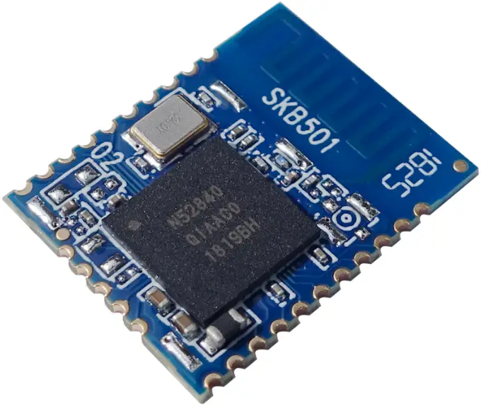
- Pin diagram
XY2612-T5 module has 3 rows of pins, a total of 33 pins, pin spacing 1.30mm.

Top view

Bottom view
(The above picture is for reference only, please refer to the actual object) - Pin definition
Interface pin definitions are shown in the following table:Pin number symbol IO type Feature 1 GND P Module power reference 2 D4 I/O Common I/O port, corresponding to PD4(Pin1) of the IC 3 B4 I/O Ordinary IO port, can do LED driverPWM output, corresponding to IC PB4 (Pin14) 4 B5 I/O Ordinary IO port, can do LED driver PWM output, corresponding to IC PB5 (Pin15) 5 B6 I/O Ordinary IO port, can do LED driver PWM output, corresponding to IC PB6 (Pin16) 6 C1 I/O Common I/O port, corresponding to PC1 of the IC (Pin21) 7 C0 I/O Common I/O port, corresponding to PC0 (Pin20) of the IC 8 NC – Hang in the air 9 GND P Module power reference 10 NC – Hang in the air 11 NC – Hang in the air 12 B1 I/O Serial port sending pin UART_TX, corresponding to PA0 (Pin6) of the IC 13 A0 I/O Serial port receiving pin UART_RX, corresponding to IC PA0 (Pin3) 14 VDD P Power supply pin of the module (typical supply voltage: 3.3V) 15 C2 I/O Ordinary IO port, can do LED driver PWM output, corresponding to IC PC2 (Pin22) 16 C3 I/O Ordinary IO port, can do LED driver PWM output, corresponding to IC PC3 (Pin23) 17 C4 AI Ordinary IO port, can be used as ADC port, 12bits ADC, corresponding to theIC PC4 (Pin24) 18 SWS I Module burn pin, corresponding to IC PA7 SWS (Pin5) 19 NC – Hang in the air 20 B1 I/O Serial port sending pin UART_TX, corresponding to PA0 (Pin6) of the IC 21 GND P Module power reference 22 GND P Module power reference 23 D2 I/O Ordinary IO port, can be used as LED driver PWM output, corresponding to IC PD2 (Pin31) 24 NC – Hang in the air 25 NC – Hang in the air 26 NC – Hang in the air 27 NC – Hang in the air 28 D3 I/O Common I/O port, corresponding to PD3 (Pin32) of the IC 29 B7 I/O Common I/O port, corresponding to PB7 (Pin17) of the IC 30 A1 I/O Common I/O port, corresponding to PA1 (Pin4) of the IC 31 D7 I/O Common I/O port, corresponding to PD7 (Pin2) of the IC 32 RST I Hardware reset pin (active low), corresponding to IC’s RESETB (Pin25) 33 GND P Module power reference lP indicates the power supply pin, I/O indicates the input and output pins, AI indicates the analog input pin, andI indicates the input pin
Electrical parameters
| Parameter entry | Detailed description |
| Operating frequency | 2402~2480MHz |
| Wireless standard | Bluetooth 5.3 |
| Data transfer rate | 1Mbps, 2Mbps |
| Antenna type | Board PCB antenna or IPX antenna interface |
| Supply voltage | 1.8-3.6V (Typical supply voltage: 3.3V) |
| Electrostatic release voltage (mannequin) | TAMB-25℃ 2KV |
| Electrostatic release voltage (machine model) | TAMB-25℃ 0.5KV |
| Operating temperature | -40℃ ~ +85℃ |
| Storage temperature | -65℃ ~ +150℃ |
RF parameters
| argument | Minimum value | Typical value | Maximum value | unit |
| Transmitting power | ||||
| RF average output power | -0.1 | dBm | ||
| 20dB modulated signal bandwidth (1M) | – | 2500 | – | KHz |
| 20dB modulated signal bandwidth (2M) | – | 1400 | – | KHz |
| Receiving sensitivity | ||||
| RX sensitivity 1Mbps | – | -96 | dBm | |
| RX sensitivity 2Mbps | – | -93 | – | dBm |
| The frequency offset error is 1Mbps | -250 | – | +300 | KHz |
| The frequency offset error is 2Mbps | -300 | – | +200 | KHz |
| Co-channel interference suppression | – | -10 | – | dB |
Power consumption in working mode
| Working condition | Maximum value (typical)) | unit |
| Continuous transmission, 10dBm output power | 21 | mA |
| Continuous reception | 6.1 | mA |
| Average value in Mesh networking state | 6.7 | mA |
| Peak value in Mesh networking state | 24.9 | mA |
| Deep Sleep mode (16KBRAM reserved) | 1.2 | μA |
| Deep Sleep mode (no RAM reserved) | 0.4 | μA |
Antenna information
- Antenna type
The XY2612-T5 module uses either an onboard PCB antenna or an IPEX antenna interface.
XY2612-T5 module default PCB onboard antenna. IPEX is used as a generation antenna base with the following structural
dimensions:
- Reduce antenna interference
To ensure optimal RF performance, it is recommended that the distance between theantenna part of the module and other metal parts be at least 15mm. If metal materials areused around the antenna in the environment, the wireless signal will be greatly attenuated, and the RF performance will be deteriorated. When designing the finishedproduct, be careful to reserve enough space for the antenna area.

Module encapsulation
XY2612-T5 module size: 13.8±0.35mm(W)×23.8±0.35mm(L)×3.0±0.15mm(H), PCBthickness 1.0mm± 0.1mm, package as shown:
Top view:

Note : The default module dimension tolerance is ±0.35mm, and the critical dimension tolerance is ±0.1mm
The round pad on the upper right of the module is the RF test point of the module, and this part of thepad is not drawn in the package library
Recommended furnace temperature curve
Please apply the SMT patch according to the reflow soldering curve. The peaktemperature is 245℃, and the reflow soldering temperature curve is shown in the figurebelow:
Refer to IPC/JEDEC standard;Peak Temperature:<250℃;Number of Times:≤2times

Module MOQ and packaging information
| Product model | antenna | MOQ(PCS) | Shipping package way | Per reel Number of packagingmodules | Each case packing Number of reels |
| XY2612-T5 | Onboardantenna | 3600 | Carrying reel | 900 | 4 |
| XY2612-T5-IPEX | Externalantenna | 3600 | Carrying reel | 900 | 4 |
List of applicable FCC rules FCC Part 15 Subpart C 15.247&15.209
Specific operational use conditions.
The module can be used for mobile applications with a maximum 0.13dBi antenna. The manufacturer installing this module into their product must ensure that the final compos it product complies with the FCC requirements by a technical assessment or evaluation to the FCC rules , including the transmitter operation . The host manufacturer has to be aware not to provide information to the end user regarding how to install or remove this RF module in the users manual of the end product which integrates this module . The end user manual shall include all required regulatory information / warming as show in this manual.
Limited module procedures. Not applicable.
The module is a Single module and complies with the requirement of FCC part 15.212.
Trace antenna designs .Not applicable .
The module as its ow antenna,and doesn’t need a host sprinted board micros trip trace antenna etc RF exposure considerations.
The module must be installed in the host equipment such that at least 20cm is maintained between the antenna and users ” body,and if RF exposure statement or module layout is changed , then the host product
manufacturer required to take responsibility of the module through a change in FCC ID or new application
. The FCC ID of the module cannot be used on the final product In these circumstance , the host manufacturer will be responsible for evaluating the end product ( including the transmitter ) and obtaining a separate FCC
authorization
Antennas : Antenna Specification are as follows :
Type : PCB Antenna
Gain : 3.5dBi Max
This device is intended only for host manufacturers under the following conditions:The module shall be only used with the PCB antennas ) that has been originally tested and certified with this module . The antenna must be either permanently attached or employ a unique antenna coupler.As long as the conditions above are met , further transmitter test will not be required However , the host manufacturer is still responsible for testing their end-product for any additional compliance requirements required with his module installed for example , digital device emissions , PC peripheral requirements , etc : )
Label and compliance information Host product manufacturers need to provide a physical or e-label stating ” Contains FCC ID:2A9TO-XY2612-T5 with their finished product.
Information on the modes and additional testing requirements Host manacor mspaorms of aiad & oced mission and spurious emission a in ac test modes for a stand – along modular transmitter inhost , as well as for multi silanus ramming modules or other transmitters in a host product.
Only when all the test results of test modes comply with FCC requirements , then the end product can be sold legally.
Additional testing,Part 15 subpart B disclaimer.The modular transmitter is only FCC authorized for FCC Part 15 Subpart C 15.247 & 15. 209 and that the host product manufacturer is responsible for compliance to any other FCC rules that apply to the host not covered by the modular transmitter grant of certification.
If the grantee markets their product as being art 15 Subpart B compliant when it also contains unintentional radiator digital circuity , then the grantee shall provide a notice stating that the final host product still requires art 15 Subpart B compliance testing
CAUTION: Any changes or modifications not expressly approved could void the user’s authority to operate the equipment.
This equipment complies with FCC radiation exposure limits set forth for an uncontrolled environment. This equipment should be installed and operated with a minimum distance of 20cm between the radiator & your body
. This transmitter must not be co-located or operating in conjunction with any other antenna or transmitter.
Any changes or modifications not expressly approved by the party responsible for compliance could void the user’s authority to operate the equipment. This device complies with Part 15 of the FCC Rules. Operation is
subject to the following two conditions: (1) this device may not cause harmful interference, and(2) this device must accept any interference received , including interference that may cause undesired operation.
Note: This equipment has been tested and found to comply with the limits for a digital device, pursuant to Part 15 of the FCC Rules. These limits are designed to provide reasonable protection against harmful interference in a residential installation. This equipment generates, uses, and can radiate radio frequency energy, and if not installed and used in accordance with the instructions, may cause harmful interference to radio communications.
However, there is no guarantee that interference will not occur in a particular installation. If this equipment does cause harmful interference to radio or television reception, which can be determined by turning the equipment off and on, the user is encouraged to try to correct the interference by one or more of the following measures:
- Reorient or relocate the receiving antenna.
- Increase the separation between the equipment and receiver.
- Connect the equipment into an outlet on a circuit different from that to which the receiver is connected.
- Consult the dealer or an experienced radio/TV technician for help.

Documents / Resources
 |
RINO XY2612-T5 Bluetooth Low Power Module [pdf] User Manual XY2612-T5 Bluetooth Low Power Module, XY2612-T5, Bluetooth Low Power Module, Low Power Module, Power Module, Module |