
NXP UM12262 Development Board User Manual
Document information

1 FRDM-IMX91 overview
The FRDM i.MX 91 development board (FRDM-IMX91 board) is a low-cost platform designed to show the most commonly used features of the i.MX 91 Applications Processor in a small and low-cost package. The FRDMIMX91 board is an entry-level development board, which helps developers to get familiar with the processor before investing a large amount of resources in more specific designs.
This document includes system setup and configurations, and provides detailed information on the overall design and usage of the FRDM board from a hardware system perspective.
1.1 Block diagram
Figure 1 shows the FRDM-IMX91 block diagram.

1.2 Board features
Table 1 lists the features of FRDM-IMX91.
Table 1. FRDM-IMX91 features


1.3 Board kit contents
Table 2 lists the items included in the FRDM-IMX91 board kit.
Table 2. Board kit contents

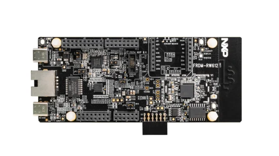
1.4 Board pictures
Figure 2 shows the top-side view of the FRDM-IMX91 board.

Figure 3 shows the connectors available on the top side of the FRDM-IMX91 board.

Figure 4 shows the onboard switches, buttons, and LEDs available on the FRDM-IMX91 board.

Figure 5 shows the bottom-side view, and also highlights the connectors available at the bottom side of the FRDM-IMX91 board.

1.5 Connectors
See Figure 3 and Figure 5 for connectors position on the board. Table 3 describes the FRDM-IMX91 board connectors.
Table 3. FRDM-IMX91 connectors


1.6 Push buttons
Figure 4 shows the push buttons available on the board.
Table 4 describes the push buttons available on FRDM-IMX91.
Table 4. FRDM-IMX91 push buttons

1.7 DIP switch
The following DIP switches are used on the FRDM-IMX91 board.
- 4-bit DIP switch – SW1
- 2-bit DIP switch – SW3
- 1-bit DIP switch – SW4
If a DIP switch pin is:
- OFF – pin value is 0
- ON – pin value is 1
The following list describes the description and configuration of the DIP switches available on the board.
• SW1 – Provides control for boot mode configuration. For detail, see Section 2.5.
• SW3 – Provides control for enabling or disabling the CAN interface signals, CAN_TXD (GPIO_IO25) and CAN_RXD (GPIO_IO27), on the board.

1.8 LEDs
The FRDM-IMX91 board has light-emitting diodes (LEDs) to monitor system functions, such as power-on and board faults. The information collected from LEDs can be used for debugging purposes.
Figure 4 shows the LEDs available on the board.
Table 7 describes the FRDM-IMX91 LEDs.
Table 7. FRDM-IMX91 LEDs

2 FRDM-IMX91 functional description
This chapter describes the features and functions of the FRDM-IMX91 board.
Note: For details of the i.MX 91 MPU features, see i.MX 91 Applications Processor Reference Manual.
The chapter is divided into the following sections:
• Section “Processor”
• Section “Power supply”
• Section “Clocks”
• Section “I2C interface”
• Section “Boot mode and boot device configuration”
• Section “PDM interface”
• Section “LPDDR4 DRAM memory”
• Section “SD card interface”
• Section “eMMC memory”
• Section “M.2 interface”
• Section “CAN interface”
• Section “USB interface”
• Section “Ethernet”
• Section “EXPI connector”
• Section “Debug interface”
• Section “Board errata”
2.1 Processor
The i.MX 91 applications processor includes single Arm Cortex-A55 processors with speeds up to 1.4 GHz.
Robust control networks are possible via the CAN-FD interface. Also, dual 1 Gbit/s Ethernet controllers, one supporting time sensitive networking (TSN), drive gateway applications with low latency.
The i.MX 91 is useful for applications such as:
• Smart home
• Building control
• Contactless HMI
• Commercial
• Healthcare
• Industrial
Each processor provides a 16-bit LPDDR4 memory interface and other interfaces for connecting peripherals, such as WLAN, Bluetooth, USB2.0, uSDHC, Ethernet, CAN, and multisensors.
For more detailed information about the processor, see the i.MX 91 data sheet and i.MX 91 Applications
Processor Reference Manual at https://www.nxp.com/imx91.
2.2 Power supply
The primary power supply to the FRDM-IMX91 board is VBUS_IN (12 V – 20 V) through USB Type-C PD connector (P1).
Three DC buck switching regulators are used:
• MP8759GD (U702) switches VBUS_IN supply to SYS_5V (5 V) power supply, which is input power supply for PCA9451AHNY PMIC (U701) and other devices on board.
• MP2147GD (U726) switches VDD_5V supply to VPCIe_3V3 (3.3 V / 4 A) for M.2 / NGFF module (P8).
• MP1605C (U730) switches VPCIe_3V3 supply to VEXT_1V8 (3.3 V / 500 mA) for onboard tri-radio module
MAYA-W476-00B (U731).
Figure 6 shows the FRDM-IMX91 power supply block diagram.

Table 8 describes different power sources available on the board.
Table 8. FRDM-IMX91 power supply devices

Table 8. FRDM-IMX91 power supply devices…continued


[2] PCA9451 BUCK1/3 dual phase default output voltage is 0.85 V.
For further details on the power sequence needed by the i.MX 91, see section “Power sequence” in the i.MX 91 Reference Manual.
2.3 Clocks
FRDM-IMX91 provides all the clocks required for the processor and peripheral interfaces. Table 9 summarizes the specifications of each clock and the component that provides it.
Table 9. FRDM-IMX91 clocks

2.4 I2C interface
The i.MX 91 processor supports a low-power inter-integrated circuit (I2C) module that supports an efficient interface to an I2C-bus as a master. The I2C provides a method of communication between a number of devices available on the FRDM-IMX91 board.
One 10-pin 2×5 2.54 mm connector P12 is provided on the board to support I2C, CAN, and ADC connections.
The developers can use the port for some specific application development.
Table 10 explains the I2C, CAN, and ADC header, P12, pinout.
Table 10. 10-pin 2×5 2.54mm I2C, CAN, and ADC header (P12) pinout

Table 11 describes the I2C devices and their I2C addresses (7-bit) on the board.
Table 11. I2C devices

2.5 Boot mode and boot device configuration
The i.MX 91 processor offers multiple boot configurations, selectable by SW1 on the FRDM-IMX91 board.
In addition, the i.MX 91 can download a program image from a USB connection when configured in serial download mode. The four dedicated BOOT MODE pins are used to select the various boot modes.
Figure 7 shows the boot mode selection switch.
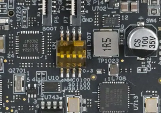
Figure 7. Boot mode selection switch
Table 12 describes the SW1 values used in different boot modes.
Table 12. Boot mode settings

On the FRDM-IMX91 board, the default boot mode is from the eMMC device. The other boot device is the microSD connector. Set SW1[3:0] as 0010 to choose uSDHC1 (eMMC) as boot device, set 0011 to choose uSDHC2 (SD), and set 0001 to enter USB serial download.
Note: For more information about the boot modes and boot device configuration, see chapter “System Boot” in the i.MX 91 Applications Processor Reference Manual.
Figure 8 shows the connection of SW1 and i.MX 91 boot mode signals.

2.6 PDM interface
The pulse density modulated (PDM) microphone interface of the processor provides PDM/MQS support on the FRDM-IMX91, and it connects to a 3.5 mm audio jack (P15).
Table 13. Audio jack

2.7 LPDDR4 DRAM memory
The FRDM-IMX91 board features one 512 M × 16 (1 channel ×16 I/O × 1 rank) LPDDR4 SDRAM chip (NT6AN512M16AV-J1) for a total of 1 GB of RAM memory. The LPDDR4 DRAM memory is connected to the i.MX 91 DRAM controller.
The ZQ calibration resistors (R209 and R2941) used by the LPDDR4 chip are 240 Ω 1% to LPD4/x_VDDQ and the ZQ calibration resistor DRAM_ZQ used at i.MX 91 SoC side is 120 Ω 1% to GND.
In the physical layout, the LPDDR4 chip is placed at the top side of the board. The data traces are not necessarily connected to the LPDDR4 chips in sequential order. Instead, the data traces are connected as best determined by the layout and other critical traces for the ease of routing.
2.8 SD card interface
The target processor has three ultra secured digital host controller (uSDHC) modules for SD/eMMC interface support. The uSDHC2 interface of the i.MX 91 processor connects to the MicroSD card slot (P13) on the FRDM-IMX91 board. This connector supports one 4-bit SD3.0 MicroSD card. To select it as the boot device of the board, see Section 2.5.
2.9 eMMC memory
The eMMC memory (at the SOM board) is connected to the uSDHC1 interface of the i.MX 91 processor, which can support eMMC 5.1 devices. It is the default boot device of the board. Table 12 describes the boot settings.
Table 14 describes the eMMC memory device that is supported by the uSDHC1 interface.
Table 14. Supported eMMC device

2.10 M.2 interface
The FRDM-IMX91 board supports the M.2/NGFF Key E mini card 75-pin connector, P8. The M.2 mini card connector supports USB, SDIO, SAI, UART, I2C, and GPIO connection. By default, these signals are connected with the onboard tri-radio MAYA-W476-00B module, however, to use this M.2 slot, the following resistors must be reworked.
Table 15. Resistors rework for M.2 slot usage

The M.2 connector can be used for Wi-Fi / Bluetooth card, IEEE 802.15.4 Radio, or 3G / 4G cards.
Table 16 describes the pinout of the M.2 mini card connector (P8).
Table 16. M.2 mini card connector (P8) pinout


2.11 Tri-radio module interface
The FRDM-IMX91 board features a Tri-radio (Wi-Fi 6, Bluetooth Low Energy 5.4, and 802.15.4) module based on the NXP IW612 that interfaces with the SD2, UART5, SAI1, and SPI3 controller of the target processor.
Table 17. Tri-radio module

The two antenna pins (RF_ANT0 and RF_ANT1) of the module connects to U.FL connectors P9 and P10 (DNP by default). The module is supplied with VPCIe_3V3, VEXT_1V8, and VDD_1V8.
The MAYA-W476-00B module and M.2 connector share several interface lines on the FRDM-IMX91 board.
Zero-ohm resistors enable signal selection between these components.
SD3 interface
The SD3 interface lines are shared between the MAYA-W476-00B module and the M.2 connector. Zero-ohm resistors select either the MAYA-W476-00B module (default setting) or the M.2 connector.
UART5 interface
Similarly, the UART5 interface lines are shared between the MAYA-W476-00B module and the M.2 connector.
Zero-ohm resistors select either the MAYA-W476-00B module (default setting) or the M.2 connector.
SAI1 interface
The SAI1 interface lines are shared between the MAYA-W476-00B module and the M.2 connector. Zero-ohm resistors select either the MAYA-W476-00B module (default setting) or the M.2 connector for 1.8 V translated signals, generated using the 74AVC4T3144 bidirectional voltage translator (U728).
SPI3 interface
The SPI3 signals (CLK, MOSI, MISO, and CS0) are multiplexed with GPIO_IO[08, 09, 10, 11] signals, respectively. These SPI3 signals are shared between the MAYA-W476-00B module and the M.2 connector.
Zero-ohm resistors select either the MAYA-W476-00B module (default setting) or the M.2 connector for 1.8 V translated signals, generated using the 74AVC4T3144 bidirectional voltage translator (U729).


2.12 CAN interface
The i.MX 91 processor supports a controller area network (CAN) module that is a communication controller implementing the CAN protocol according to the CAN with flexible data rate (CAN FD) protocol and the CAN 2.0B protocol specification. The processor supports two CAN FD controllers.
On the FRDM-IMX91 board, one of the controllers is connected to the high-speed CAN transceiver
TJA1051T/3. The high-speed CAN transceiver drives CAN signals between the target processor and a 10-pin 2×5 2.54 mm header (P12) to its physical two-wire CAN bus.
The CAN_TXD and CAN_RXD signals are multiplexed on GPIO_IO25 and GPIO_IO27, respectively. On the board, a 2-bit DIP switch (SW3) is used to control the CAN signals. For SW3 detail, see Section 1.7. The CAN_STBY signal from the IO expander PCAL6524HEAZ (U725, P2_7, I2C address: 22) enables / disables CAN standby mode.
The CAN interface circuit includes the split termination RC filter (62Ω + 56pF) for noise rejection and signal integrity. The switch SW4 is provided for enabling/disabling the RC filter. For SW4 detail, see Section 1.7.
The HS-CAN transceiver and header are described in Table 18.
Table 18. High-speed CAN transceiver and header

Note: For details about TJA1051, see TJA1051 data sheet at nxp.com.
2.13 USB interface
The i.MX 91 applications processor features two USB 2.0 controllers, with two integrated USB PHYs. On the FRDM-IMX91 board, one is used for the USB2.0 Type-C Port (P2) and the other is used for USB2.0 Type-A Port (P17).
Table 19 describes the USB ports available on the board.
Table 19. USB ports

2.14 Ethernet
The i.MX 91 processor supports two Gigabit Ethernet controllers (capable of simultaneous operation) with support for Energy-Efficient Ethernet (EEE), Ethernet AVB, and IEEE 1588.
The Ethernet subsystem of the board is provided by the Motorcomm YT8521SH-CA Ethernet transceivers (U713, U716) which support RGMII and connect to RJ45 connectors (P3, P4). The Ethernet transceivers (or PHYs) receive standard RGMII Ethernet signals from i.MX 91. The RJ45 connectors integrate Magnetic transformer inside, so they can be directly connected to Ethernet transceivers (or PHYs).
Each Ethernet port has a unique MAC address, which is fused into i.MX 91. The Ethernet connectors are labeled clearly on the board.
2.15 EXPI connector
One 2×20-pin EXPI connector (P11) is provided on the FRDM-IMX91 board to support I2S, UART, I2C, and GPIO connections. The header can be used to access various pins or to plug in accessory cards, such as the LCD display TM050RDH03-41, 8MIC-RPI-MX8 card, and MX93AUD-HAT.
The connector is shown in Figure 3.
Table 20. P11 pin definition

2.16 Debug interface
The FRDM-IMX91 board features two independent debug interfaces.
• Serial wire debug (SWD) header (Section 2.16.1)
• USB-to-dual UART debug port (Section 2.16.2)
2.16.1 SWD interface
The i.MX 91 applications processor has two serial wire debug (SWD) signals on dedicated pins, and those signals are directly connected to the standard 3-pin 2.54 mm connector P14. The two SWD signals used by the processor are:
• SWCLK (serial wire clock)
• SWDIO (serial wire data input / output)
The SWD connector P14 is shown in Figure 3.
2.16.2 USB debug interface
The i.MX 91 applications processor has six independent UART ports (UART1 – UART6). On the FRDM-IMX91 board, UART1 is used for Cortex-A55 core. A single chip USB to dual UART is used for the debug purpose. The part number is CH342F. You can download the driver from WCH Website.
After installing the CH342F driver, the PC / USB host enumerates two COM ports connected to the P16 connector through a USB cable:
- COM Port 1: Cortex-A55 system debugging
- COM Port 2: Reserved
You can use the following terminal tools for debugging purposes:
- Putty
- Tera Term
- Xshell
- Minicom>=2.9
To debug under Linux, make sure CH342F Linux driver is installed.
Table 21 describes the required settings.
Table 21. Terminal setting parameters

The USB debug connector P16 is shown in Figure 3.
2.17 Board errata
No board errata.
3 Working with accessories
This section describes how a connection can be established between with the FRDM-IMX91 board and compatible accessory boards.
3.1 5-inch Tianma LCD
TM050RDH03-41 is a 5” TFT LCD display with 800×480 resolution. This industrial-grade display uses an RGB interface without a touch panel. This display module connects to the FRDM-IMX91 through the EXPI 2×20-pin connector (P11).
3.1.1 Connection between Tianma panel and adapter board
Figure 11 shows the FPC connection between the 5-inch Tianma LCD panel and adapter board. Insert the FPC connector with the conductive side up (stiffener side down).

Figure 11. FPC connection between 5-inch Tianma LCD panel and adapter board
3.1.2 Connection between adapter board and FRDM-IMX91
Plug 5’’ Tianma LCD to FRDM-IMX91 through the EXPI 2×20-pin connector (P11) as shown in Figure 12

3.1.3 Software configuration update
The following steps specify how to replace the default dtb with the custom dtb (imx91-11×11-frdm-tianma-wvgapanel. dtb) that supports Tianma LCD.
1. Stop at U-Boot
2. Use the below commands to replace the default dtb:

3.2 Other accessory boards
There are other accessory boards also that can work with FRDM-IMX91 through EXPI 2×20-pin interface, such as 8MIC-RPI-MX8 and MX93AUD-HAT. To use any such board, check the schematic and layout to determine the direction of the connection between FRDM-IMX91 and the accessory board in advance. Also, choose the right dtb file in the U-Boot stage.

3.2.1 Software configuration update

4 PCB information
The FRDM-IMX91 is made with standard 10-layer technology. The material is FR-4, and the PCB stack-up information is described in Table 22.
Table 22. FRDM-IMX91 board stack up information


5 European Union regulatory compliance
Table 23 is provided as per Article 10.8 of the Radio Equipment Directive 2014/53/EU.
(a) Frequency bands in which the equipment operates.
(b) The maximum RF power transmitted.
Table 23. EU regulatory compliance

EUROPEAN DECLARATION OF CONFORMITY (Simplified DoC per Article 10.9 of the Radio Equipment Directive 2014/53/EU)
This apparatus, namely FRDM-IMX91 Freedom Development Platform, conforms to the Radio Equipment Directive 2014/53/EU. The full EU Declaration of Conformity for this apparatus can be found at the NXP website: FRDM-IMX91.
6 Acronyms
Table 24 lists and explains the acronyms and abbreviations used in this document.
Table 24. Acronyms


Table 25 lists and explains the additional documents and resources that you can refer to for more information on the FRDM-IMX91 board. Some of the documents listed below may be available only under a nondisclosure agreement (NDA). To request access to these documents, contact your local field applications engineer (FAE) or sales representative.
Table 25. Related documentation

8 Note about the source code in the document
The example code shown in this document has the following copyright and BSD-3-Clause license:
Copyright 2025 NXP Redistribution and use in source and binary forms, with or without modification, are permitted provided that the following conditions are met:
- Redistributions of source code must retain the above copyright notice, this list of conditions and the following disclaimer.
- Redistributions in binary form must reproduce the above copyright notice, this list of conditions and the following disclaimer in the documentation and/or other materials provided with the distribution.
- Neither the name of the copyright holder nor the names of its contributors may be used to endorse or promote products derived from this software without specific prior written permission.
THIS SOFTWARE IS PROVIDED BY THE COPYRIGHT HOLDERS AND CONTRIBUTORS “AS IS” AND ANY EXPRESS OR IMPLIED WARRANTIES, INCLUDING, BUT NOT LIMITED TO, THE IMPLIED WARRANTIES OF MERCHANTABILITY AND FITNESS FOR A PARTICULAR PURPOSE ARE DISCLAIMED. IN NO EVENT SHALL THE COPYRIGHT HOLDER OR CONTRIBUTORS BE LIABLE FOR ANY DIRECT, INDIRECT, INCIDENTAL, SPECIAL, EXEMPLARY, OR CONSEQUENTIAL DAMAGES (INCLUDING, BUT NOT LIMITED TO, PROCUREMENT OF SUBSTITUTE GOODS OR SERVICES; LOSS OF USE, DATA, OR PROFITS; OR BUSINESS INTERRUPTION) HOWEVER CAUSED AND ON ANY THEORY OF LIABILITY, WHETHER IN CONTRACT, STRICT LIABILITY, OR TORT (INCLUDING NEGLIGENCE OR OTHERWISE) ARISING IN ANY WAY OUT OF THE USE OF THIS SOFTWARE, EVEN IF ADVISED OF THE POSSIBILITY OF SUCH DAMAGE.
9 Revision history
Table 26 summarizes the revisions to this document.

Legal information
Definitions
Draft — A draft status on a document indicates that the content is still under internal review and subject to formal approval, which may result in modifications or additions. NXP Semiconductors does not give any representations or warranties as to the accuracy or completeness of information included in a draft version of a document and shall have no liability for the consequences of use of such information.
Disclaimers
Limited warranty and liability — Information in this document is believed to be accurate and reliable. However, NXP Semiconductors does not give any representations or warranties, expressed or implied, as to the accuracy or completeness of such information and shall have no liability for the consequences of use of such information. NXP Semiconductors takes no responsibility for the content in this document if provided by an information source outside of NXP Semiconductors.
In no event shall NXP Semiconductors be liable for any indirect, incidental, punitive, special or consequential damages (including – without limitation – lost profits, lost savings, business interruption, costs related to the removal or replacement of any products or rework charges) whether or not such damages are based on tort (including negligence), warranty, breach of contract or any other legal theory.
Notwithstanding any damages that customer might incur for any reason whatsoever, NXP Semiconductors’ aggregate and cumulative liability towards customer for the products described herein shall be limited in accordance with the Terms and conditions of commercial sale of NXP Semiconductors.
Right to make changes — NXP Semiconductors reserves the right to make changes to information published in this document, including without limitation specifications and product descriptions, at any time and without notice. This document supersedes and replaces all information supplied prior to the publication hereof.
Suitability for use — NXP Semiconductors products are not designed, authorized or warranted to be suitable for use in life support, life-critical or safety-critical systems or equipment, nor in applications where failure or malfunction of an NXP Semiconductors product can reasonably be expected to result in personal injury, death or severe property or environmental damage. NXP Semiconductors and its suppliers accept no liability for inclusion and/or use of NXP Semiconductors products in such equipment or applications and therefore such inclusion and/or use is at the customer’s own risk.
Applications — Applications that are described herein for any of these products are for illustrative purposes only. NXP Semiconductors makes no representation or warranty that such applications will be suitable for the specified use without further testing or modification.
Customers are responsible for the design and operation of their applications and products using NXP Semiconductors products, and NXP Semiconductors accepts no liability for any assistance with applications or customer product design. It is customer’s sole responsibility to determine whether the NXP Semiconductors product is suitable and fit for the customer’s applications and products planned, as well as for the planned application and use of customer’s third party customer(s). Customers should provide appropriate design and operating safeguards to minimize the risks associated with their applications and products.
NXP Semiconductors does not accept any liability related to any default, damage, costs or problem which is based on any weakness or default in the customer’s applications or products, or the application or use by customer’s third party customer(s). Customer is responsible for doing all necessary testing for the customer’s applications and products using NXP Semiconductors products in order to avoid a default of the applications and the products or of the application or use by customer’s third party customer(s). NXP does not accept any liability in this respect.
Terms and conditions of commercial sale — NXP Semiconductors products are sold subject to the general terms and conditions of commercial sale, as published at https://www.nxp.com/profile/terms, unless otherwise agreed in a valid written individual agreement. In case an individual agreement is concluded only the terms and conditions of the respective agreement shall apply. NXP Semiconductors hereby expressly objects to applying the customer’s general terms and conditions with regard to the purchase of NXP Semiconductors products by customer.
Export control — This document as well as the item(s) described herein may be subject to export control regulations. Export might require a prior authorization from competent authorities.
Suitability for use in non-automotive qualified products — Unless this document expressly states that this specific NXP Semiconductors product is automotive qualified, the product is not suitable for automotive use. It is neither qualified nor tested in accordance with automotive testing or application requirements. NXP Semiconductors accepts no liability for inclusion and/or use of non-automotive qualified products in automotive equipment or applications.
In the event that customer uses the product for design-in and use in automotive applications to automotive specifications and standards, customer (a) shall use the product without NXP Semiconductors’ warranty of the product for such automotive applications, use and specifications, and (b) whenever customer uses the product for automotive applications beyond NXP Semiconductors’ specifications such use shall be solely at customer’s own risk, and (c) customer fully indemnifies NXP Semiconductors for any liability, damages or failed product claims resulting from customer design and use of the product for automotive applications beyond NXP Semiconductors’ standard warranty and NXP Semiconductors’ product specifications.
Evaluation products — This evaluation product is intended solely for technically qualified professionals, specifically for use in research and development environments to facilitate evaluation purposes. It is not a finished product, nor is it intended to be a part of a finished product. Any software or software tools provided with an evaluation product are subject to the applicable license terms that accompany such software or software tools.
This evaluation product is provided on an “as is” and “with all faults” basis for evaluation purposes only and is not to be used for product qualification or production. If you choose to use these evaluation products, you do so at your risk and hereby agree to release, defend and indemnify NXP (and all of its affiliates) for any claims or damages resulting from your use.
NXP, its affiliates and their suppliers expressly disclaim all warranties, whether express, implied or statutory, including but not limited to the implied warranties of non-infringement, merchantability and fitness for a particular purpose. The entire risk as to the quality, or arising out of the use or performance, of this evaluation product remains with user.
In no event shall NXP, its affiliates or their suppliers be liable to user for any special, indirect, consequential, punitive or incidental damages (including without limitation damages for loss of business, business interruption, loss of use, loss of data or information, and the like) arising out the use of or inability to use the evaluation product, whether or not based on tort (including negligence), strict liability, breach of contract, breach of warranty or any other theory, even if advised of the possibility of such damages.
Notwithstanding any damages that user might incur for any reason whatsoever (including without limitation, all damages referenced above and all direct or general damages), the entire liability of NXP, its affiliates and their suppliers and user’s exclusive remedy for all of the foregoing shall be limited to actual damages incurred by user based on reasonable reliance up to the greater of the amount actually paid by user for the evaluation product or five dollars (US$5.00). The foregoing limitations, exclusions and disclaimers shall apply to the maximum extent permitted by applicable law, even if any remedy fails of its essential purpose and shall not apply in case of willful misconduct.
HTML publications — An HTML version, if available, of this document is provided as a courtesy. Definitive information is contained in the applicable document in PDF format. If there is a discrepancy between the HTML document and the PDF document, the PDF document has priority.
Translations — A non-English (translated) version of a document, including the legal information in that document, is for reference only. The English version shall prevail in case of any discrepancy between the translated and English versions.
Security — Customer understands that all NXP products may be subject to unidentified vulnerabilities or may support established security standards or specifications with known limitations. Customer is responsible for the design and operation of its applications and products throughout their lifecycles to reduce the effect of these vulnerabilities on customer’s applications and products. Customer’s responsibility also extends to other open and/or proprietary technologies supported by NXP products for use in customer’s applications. NXP accepts no liability for any vulnerability. Customer should regularly check security updates from NXP and follow up appropriately.
Customer shall select products with security features that best meet rules, regulations, and standards of the intended application and make the ultimate design decisions regarding its products and is solely responsible for compliance with all legal, regulatory, and security related requirements concerning its products, regardless of any information or support that may be provided by NXP.
NXP has a Product Security Incident Response Team (PSIRT) (reachable at PSIRT@nxp.com) that manages the investigation, reporting, and solution release to security vulnerabilities of NXP products.
NXP B.V. — NXP B.V. is not an operating company and it does not distribute or sell products.
Trademarks
Notice: All referenced brands, product names, service names, and trademarks are the property of their respective owners.
NXP — wordmark and logo are trademarks of NXP B.V.
AMBA, Arm, Arm7, Arm7TDMI, Arm9, Arm11, Artisan, big.LITTLE,
Cordio, CoreLink, CoreSight, Cortex, DesignStart, DynamIQ, Jazelle,
Keil, Mali, Mbed, Mbed Enabled, NEON, POP, RealView, SecurCore,
Socrates, Thumb, TrustZone, ULINK, ULINK2, ULINK-ME, ULINKPLUS, ULINKpro, μVision, Versatile — are trademarks and/or registered trademarks of Arm Limited (or its subsidiaries or affiliates) in the US and/or elsewhere. The related technology may be protected by any or all of patents, copyrights, designs and trade secrets. All rights reserved.
Bluetooth — the Bluetooth wordmark and logos are registered trademarks owned by Bluetooth SIG, Inc. and any use of such marks by NXP Semiconductors is under license.
UM12262
Please be aware that important notices concerning this document and the product(s) described herein, have been included in section ‘Legal information’.
© 2025 NXP B.V.
For more information, please visit: https://www.nxp.com
All rights reserved.
For more information, please visit: https://www.nxp.com Document feedback
Date of release: 22 April 2025
Document identifier: UM12262
Read More About This Manual & Download PDF:
Documents / Resources
 |
NXP UM12262 Development Board [pdf] User Manual i.MX 91, FRDM-IMX91, UM12262, UM12262 Development Board, UM12262, Development Board, Board |