ALPHA DATA FMC-PLUS-QSFP-DD Compatible Digital Input Output Board
Product Information
The FMC-PLUS-QSFP-DD is a high-speed serial IO (HSSIO) module designed by Alpha Data Parallel Systems Ltd. It provides users with the ability to connect and communicate with QSFP-DD connectors. The module offers various features and functionalities to enhance data transmission and connectivity.
Specifications
- Revision: 1.1
- Publication Date: 22nd March 2023
- Copyright: Protected by Copyright Law
- Manufacturer: Alpha Data Parallel Systems Ltd.
- Head Office Address: Suite L4A, 160 Dundee Street, Edinburgh, EH11 1DQ, UK
- Head Office Telephone: +44 131 558 2600
- Head Office Fax: +44 131 558 2700
- Head Office Email: sales@alpha-data.com
- Head Office Website: http://www.alpha-data.com
- US Office Address: 10822 West Toller Drive, Suite 250 Littleton, CO 80127
- US Office Telephone: (303) 954 8768
- US Office Toll-Free Telephone: (866) 820 9956
- US Office Email: sales@alpha-data.com
- US Office Website: http://www.alpha-data.com
Product Usage Instructions
Introduction
The FMC-PLUS-QSFP-DD module is designed to enhance high-speed serial IO capabilities. It is important to refer to the user manual for detailed instructions on installation and usage.
References & Specifications
For detailed references and specifications, please refer to the user manual provided with the module.
High-Speed Serial IO (HSSIO)
The FMC-PLUS-QSFP-DD module supports high-speed serial IO connections. It allows users to transmit data at high speeds for various applications.
User Clock
The module provides a user clock feature that enables synchronization and timing control for data transmission. Refer to the user manual for instructions on utilizing the user clock functionality.
Connectors
The module is equipped with QSFP-DD connectors for seamless and reliable connectivity. Ensure proper cable mating for optimal performance.
Mating Cables
Refer to the user manual for recommended mating cables to ensure compatibility and reliable data transmission.
Installation
Proper installation of the FMC-PLUS-QSFP-DD module is crucial for optimal performance and functionality.
Handling Instructions
Follow the handling instructions provided in the user manual to prevent damage to the module during installation or maintenance.
IO Voltage Selection
Refer to the user manual for instructions on selecting the appropriate IO voltage for your specific application.
Appendix A: FMC+ Pin Assignments
For detailed pin assignments, refer to Appendix A in the user manual.
A.1 Clock Signals
Appendix A provides information on the pin assignments related to clock signals. Ensure proper configuration for accurate timing control.
A.2 High-Speed Serial IO
Refer to Appendix A for pin assignments related to high-speed serial IO connections. This information is crucial for proper data transmission and connectivity.
Appendix B: Alpha Data GPIO Pin Assignments
For detailed GPIO pin assignments, refer to Appendix B in the user manual. This information is useful for configuring GPIO functionality.
List of Tables
- Table 1: FMC-PLUS-QSFP-DD Image
- Table 2: FMC-PLUS-QSFP-DD Block Diagram
- Table 3: FMC-PLUS-QSFP-DD Top Side Features
List of Figures
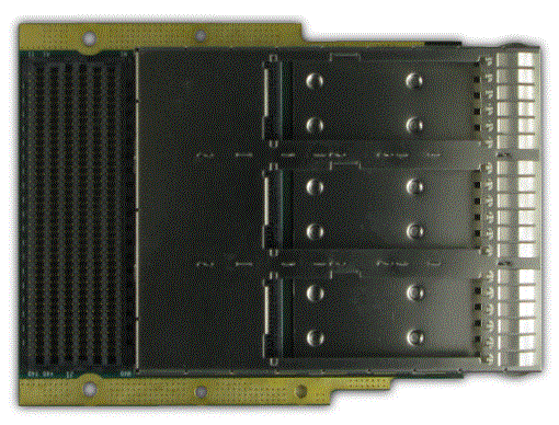
- Figure 1: FMC-PLUS_QSFP-DD Image
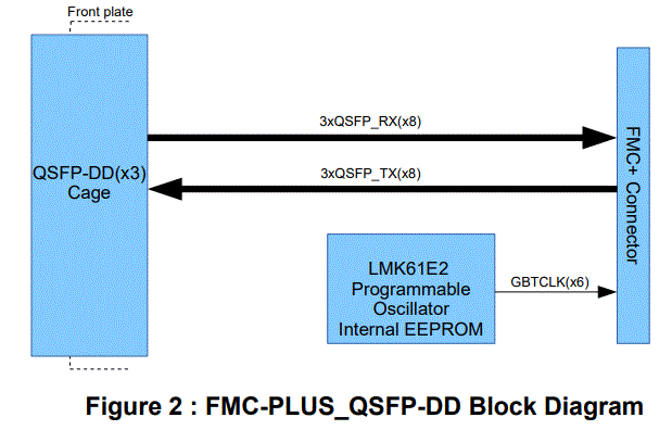
- Figure 2: FMC-PLUS_QSFP-DD Block Diagram
- Figure 3: FMC-PLUS-QSFP-DD Top Side Features
© 2023 Copyright Alpha Data Parallel Systems Ltd.
All rights reserved.
This publication is protected by Copyright Law, with all rights reserved. No part of this publication may be reproduced, in any shape or form, without prior written consent from Alpha Data Parallel Systems Ltd.
Head Office
Address: Suite L4A, 160 Dundee Street,
Edinburgh, EH11 1DQ, UK
Telephone: +44 131 558 2600
Fax: +44 131 558 2700
email: sales@alpha-data.com
website: http://www.alpha-data.com
US Office
10822 West Toller Drive, Suite 250 Littleton, CO 80127
(303) 954 8768
(866) 820 9956 – toll free sales@alpha-data.com
http://www.alpha-data.com
All trademarks are the property of their respective owners.
Introduction
The FMC-PLUS-QSFP-DD is a VITA 57.4 compliant Single Width HSPC FMC Plus module, designed for use with Alpha Data’s VITA 57.4 compliant carrier cards. It provides the user with the connectivity to implement high-speed serial IO communication applications. This adapter board provides the connection between the FPGA card and industry-standard 3xQSFP Double Density connectors. Maximum total bandwidth = 600Gbps (28Gbps per channel per direction)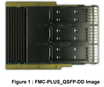
Key Features
- FMC (VITA 57.4) electrically compliant
- The FMC-PLUS-QSFP-DD module is based on VITA 57.4 but does not adhere to the mechanical specification(Region 1 of VITA 57.4 is extended to 7.1mm from 5.2mm and the IO Area is extended both in width and depth to be able to fit the 3xQSFP-DD connectors)
- Air-cooled compatible
- Each cage has 8 lanes of up to 28Gbps Series capable of 2x100GE, or 8x10GE, and many other signaling standards
- Operating temperature ranges from 0 to 55 degrees Celsius
- Compatible with active optical cables
References & Specifications

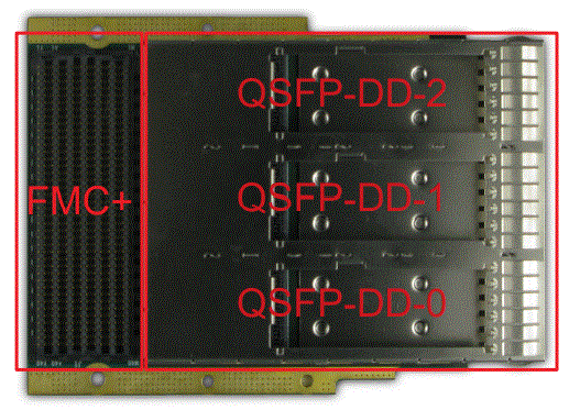 Figure 3 : FMC-PLUS-QSFP-DD Top Side Features
High Speed Serial IO
(HSSIO)
User Clock
The user can specify a custom clock frequency from the on-board Programmable Oscillator With Internal EEPROM(LMK61E2) that is directed to the FPGA banks associated with the high speed serial signals from this module. This enables support for a multitude of high speed serial IO communication protocols.
Connectors
The QSFP DD connectors on the FMC-PLUS-QSFP-DD offers the user a wide selection of interconnect schemes that break out the multi-gigabit transceivers on the FPGA.
Receptacle
- QSFP-DD connector/cage system: Molex part number 202718-0100
Mating Cables
Below is a list of possible mating cables for the QSFP-DD receptacle/cage: Cable Solutions
- For passive cables use Molex 2015911005 or similar
Installation
The FMC-PLUS-QSFP-DD is designed to plug into the FMC+ front panel connector on a compatible carrier. The retaining screws should be tightened to secure the FMC+.
The FMC-PLUS-QSFP-DD it should be removed in a certain way for the FMC+ connector not to be damaged. Here is a video from Samtec showing the removal procedure of this kind of connectors: see https://vimeo.com/158484280
Note:
This operation should not be performed while the host carrier is powered.
Handling instructions
Observe precautions for preventing damage to components by electrostatic discharge. Personnel handling the board should take SSD precautions and avoid flexing the board.
IO Voltage Selection
The required IO voltage range (VADJ) for the FMC+ is 1.2V to 3.3V. This is stored in a ROM on the FMC+, as per VITA 57.4 for automatic configuration of supplies. The carrier is responsible for detecting and setting the IO voltage accordingly.
Appendix A: FMC+ Pin Assignments
Appendix A.1: Clock Signals
| FMC Signal | FMC (J1) | Function | | | Function | FMC (J1) | FMC Signal |
| GBTCLK0_M2C_P* | D4 | USER_CLK_P | | | USER_CLK_N | D5 | GBTCLK0_M2C_N* |
| GBTCLK1_M2C_P* | B20 | USER_CLK_P | | | USER_CLK_N | B21 | GBTCLK1_M2C_N* |
| GBTCLK2_M2C_P* | L12 | USER_CLK_P | | | USER_CLK_N | L13 | GBTCLK2_M2C_N* |
| GBTCLK3_M2C_P* | L8 | USER_CLK_P | | | USER_CLK_N | L9 | GBTCLK3_M2C_N* |
| GBTCLK4_M2C_P* | L4 | USER_CLK_P | | | USER_CLK_N | L5 | GBTCLK4_M2C_N* |
| GBTCLK5_M2C_P* | Z20 | USER_CLK_P | | | USER_CLK_N | Z21 | GBTCLK5_M2C_N* |
Appendix A.2: High Speed Serial IO
| FMC Signal | FMC (J1) | Function | | | Function | FMC (J1) | FMC Signal |
| DP0_M2C_P | C6 | QSFP_0_RX_P0 | | | QSFP_0_TX_P0 | C2 | DP0_C2M_P |
| DP0_M2C_N | C7 | QSFP_0_RX_N0 | | | QSFP_0_TX_N0 | C3 | DP0_C2M_N |
| DP1_M2C_P | A2 | QSFP_0_RX_P1 | | | QSFP_0_TX_P1 | A22 | DP1_C2M_P |
| DP1_M2C_N | A3 | QSFP_0_RX_N1 | | | QSFP_0_TX_N1 | A23 | DP1_C2M_N |
| DP2_M2C_P | A6 | QSFP_0_RX_P2 | | | QSFP_0_TX_P2 | A26 | DP2_C2M_P |
| DP2_M2C_N | A7 | QSFP_0_RX_N2 | | | QSFP_0_TX_N2 | A27 | DP2_C2M_N |
| DP3_M2C_P | A10 | QSFP_0_RX_P3 | | | QSFP_0_TX_P3 | A30 | DP3_C2M_P |
| DP3_M2C_N | A11 | QSFP_0_RX_N3 | | | QSFP_0_TX_N3 | A31 | DP3_C2M_N |
| DP4_M2C_P | A14 | QSFP_0_RX_P4 | | | QSFP_0_TX_P4 | A34 | DP4_C2M_P |
| DP4_M2C_N | A15 | QSFP_0_RX_N4 | | | QSFP_0_TX_N4 | A35 | DP4_C2M_N |
| DP5_M2C_P | A18 | QSFP_0_RX_P5 | | | QSFP_0_TX_P5 | A38 | DP5_C2M_P |
| DP5_M2C_N | A19 | QSFP_0_RX_N5 | | | QSFP_0_TX_N5 | A39 | DP5_C2M_N |
| DP6_M2C_P | B16 | QSFP_0_RX_P6 | | | QSFP_0_TX_P6 | B36 | DP6_C2M_P |
| DP6_M2C_N | B17 | QSFP_0_RX_N6 | | | QSFP_0_TX_N6 | B37 | DP6_C2M_N |
| DP7_M2C_P | B12 | QSFP_0_RX_P7 | | | QSFP_0_TX_P7 | B32 | DP7_C2M_P |
| DP7_M2C_N | B13 | QSFP_0_RX_N7 | | | QSFP_0_TX_N7 | B33 | DP7_C2M_N |
| DP8_M2C_P | B8 | QSFP_1_RX_P0 | | | QSFP_1_TX_P0 | B28 | DP8_C2M_P |
| DP8_M2C_N | B9 | QSFP_1_RX_N0 | | | QSFP_1_TX_N0 | B29 | DP8_C2M_N |
| DP9_M2C_P | B4 | QSFP_1_RX_P1 | | | QSFP_1_TX_P1 | B24 | DP9_C2M_P |
| DP9_M2C_N | B5 | QSFP_1_RX_N1 | | | QSFP_1_TX_N1 | B25 | DP9_C2M_N |
| DP10_M2C_P | Y10 | QSFP_1_RX_P2 | | | QSFP_1_TX_P2 | Z24 | DP10_C2M_P |
| DP10_M2C_N | Y11 | QSFP_1_RX_N2 | | | QSFP_1_TX_N2 | Z25 | DP10_C2M_N |
Table 3 : Serial Channel Locations (continued on next page)
| FMC Signal | FMC (J1) | Function | | | Function | FMC (J1) | FMC Signal |
| DP11_M2C_P | Z12 | QSFP_1_RX_P3 | | | QSFP_1_TX_P3 | Y26 | DP11_C2M_P |
| DP11_M2C_N | Z13 | QSFP_1_RX_N3 | | | QSFP_1_TX_N3 | Y27 | DP11_C2M_N |
| DP12_M2C_P | Y14 | QSFP_1_RX_P4 | | | QSFP_1_TX_P4 | Z28 | DP12_C2M_P |
| DP12_M2C_N | Y15 | QSFP_1_RX_N4 | | | QSFP_1_TX_N4 | Z29 | DP12_C2M_N |
| DP13_M2C_P | Z16 | QSFP_1_RX_P5 | | | QSFP_1_TX_P5 | Y30 | DP13_C2M_P |
| DP13_M2C_N | Z17 | QSFP_1_RX_N5 | | | QSFP_1_TX_N5 | Y31 | DP13_C2M_N |
| DP14_M2C_P | Y18 | QSFP_1_RX_P6 | | | QSFP_1_TX_P6 | M18 | DP14_C2M_P |
| DP14_M2C_N | Y19 | QSFP_1_RX_N6 | | | QSFP_1_TX_N6 | M19 | DP14_C2M_N |
| DP15_M2C_P | Y22 | QSFP_1_RX_P7 | | | QSFP_1_TX_P7 | M22 | DP15_C2M_P |
| DP15_M2C_N | Y23 | QSFP_1_RX_N7 | | | QSFP_1_TX_N7 | M23 | DP15_C2M_N |
| DP16_M2C_P | Z32 | QSFP_2_RX_P0 | | | QSFP_2_TX_P0 | M26 | DP16_C2M_P |
| DP16_M2C_N | Y33 | QSFP_2_RX_N0 | | | QSFP_2_TX_N0 | M27 | DP16_C2M_N |
| DP17_M2C_P | Y34 | QSFP_2_RX_P1 | | | QSFP_2_TX_P1 | M30 | DP17_C2M_P |
| DP17_M2C_N | Y35 | QSFP_2_RX_N1 | | | QSFP_2_TX_N1 | M31 | DP17_C2M_N |
| DP18_M2C_P | Z36 | QSFP_2_RX_P2 | | | QSFP_2_TX_P2 | M34 | DP18_C2M_P |
| DP18_M2C_N | Z37 | QSFP_2_RX_N2 | | | QSFP_2_TX_N2 | M35 | DP18_C2M_N |
| DP19_M2C_P | Y38 | QSFP_2_RX_P3 | | | QSFP_2_TX_P3 | M38 | DP19_C2M_P |
| DP19_M2C_N | Y39 | QSFP_2_RX_N3 | | | QSFP_2_TX_N3 | M39 | DP19_C2M_N |
| DP20_M2C_P | M14 | QSFP_2_RX_P4 | | | QSFP_2_TX_P4 | Z8 | DP20_C2M_P |
| DP20_M2C_N | M15 | QSFP_2_RX_N4 | | | QSFP_2_TX_N4 | Z9 | DP20_C2M_N |
| DP21_M2C_P | M10 | QSFP_2_RX_P5 | | | QSFP_2_TX_P5 | Y6 | DP21_C2M_P |
| DP21_M2C_N | M11 | QSFP_2_RX_N5 | | | QSFP_2_TX_N5 | Y7 | DP21_C2M_N |
| DP22_M2C_P | M6 | QSFP_2_RX_P6 | | | QSFP_2_TX_P6 | Z4 | DP22_C2M_P |
| DP22_M2C_N | M7 | QSFP_2_RX_N6 | | | QSFP_2_TX_N6 | Z5 | DP22_C2M_N |
| DP23_M2C_P | M2 | QSFP_2_RX_P7 | | | QSFP_2_TX_P7 | Y2 | DP23_C2M_P |
| DP23_M2C_N | M3 | QSFP_2_RX_N7 | | | QSFP_2_TX_N7 | BY3 | DP23_C2M_N |
Table 3 : Serial Channel Locations
Note:
The function names match the QSFP-DD connectors name
Appendix B: Alpha Data GPIO Pin Assignments
| FMC Signal | FMC (J1) | Function |
| LA02_P | H7 | QSFP_0_SCL |
| LA03_P | G9 | QSFP_0_SDA |
| LA04_P | H10 | QSFP_0_RST_L |
| LA05_P | D11 | QSFP_0_LPMODE |
| LA06_P | C10 | QSFP_0_INT_L |
| LA07_P | H13 | QSFP_0_MODPRS_L |
| LA08_P | G12 | QSFP_1_SCL |
| LA09_P | D14 | QSFP_1_SDA |
| LA010_P | C14 | QSFP_1_RST_L |
| LA011_P | G15 | QSFP_1_LPMODE |
| LA012_P | H16 | QSFP_1_INT_L |
| LA013_P | D17 | QSFP_1_MODPRS_L |
| LA014_P | C18 | QSFP_2_SCL |
| LA015_P | H19 | QSFP_2_SDA |
| LA016_P | G18 | QSFP_2_RST_L |
| LA019_P | H22 | QSFP_2_LPMODE |
| LA020_P | G21 | QSFP_2_INT_L |
| LA021_P | H25 | QSFP_2_MODPRS_L |
| LA022_P | G23 | FPGA_SCL |
| LA023_P | D24 | FPGA_SDA |
| FMC_SCL | C30 | FMC_SCL |
| FMC_SDA | C31 | FMC_SDA |
Table 4 : GPIO Locations
Revision History
| Date | Revision | Changed By | Nature of Change |
| 20 Jul 2021 | 1.0 | A. Kapouranis | Initial Release |
| 22 Mar 2023 | 1.1 | A. Kapouranis | Changed Top Side Features image to show QSFP-DD 0-2 |
Address: Suite L4A, 160 Dundee Street,
Edinburgh, EH11 1DQ, UK
Telephone: +44 131 558 2600
Fax: +44 131 558 2700
email: sales@alpha-data.com
website: http://www.alpha-data.com
Address: 10822 West Toller Drive, Suite 250
Littleton, CO 80127
Telephone: (303) 954 8768
Fax: (866) 820 9956 – toll free
email: sales@alpha-data.com
website: http://www.alpha-data.com
Documents / Resources
 |
ALPHA DATA FMC-PLUS-QSFP-DD Compatible Digital Input Output Board [pdf] User Manual FMC-PLUS-QSFP-DD Compatible Digital Input Output Board, FMC-PLUS-QSFP-DD, Compatible Digital Input Output Board, Digital Input Output Board, Input Output Board, Output Board, Board |