RENESAS DA14535MOD SmartBond TINY Bluetooth LE Module

Product Information
Specifications:
- Model: DA14535MOD
- Standards Conformance:
- Europe (CE/RED)
- UK (UKCA)
- US (FCC)
- Canada (IC)
- Japan (MIC)
- South Korea (KCC)
- Taiwan (NCC)
- Brazil (Anatel)
- South Africa (ICASA)
- China (SRRC)
- Thailand (NBTC)
- India (WPC)
- Australia/ New Zealand (ACMA)
- Revision: 1.5-DRAFT
- Date: 28-Sept-2023
Key Features:
- Confidential
- Target: Beacons, Remote Controls, Proximity tags, Low Power Sensors, Commissioning/Provisioning, RF pipe, Toys, Industrial applications, Data acquisition, Wellness, Infotainment, IoT, Robotics, Gaming
Applications:
- Beacons
- Remote Controls
- Proximity tags
- Low Power Sensors
- Commissioning/Provisioning
- RF pipe
- Toys
- Industrial applications
- Data acquisition
- Wellness
- Infotainment
- IoT
- Robotics
- Gaming
Product Usage Instructions
- References
The references section provides additional information and resources related to the product. Please refer to this section for further guidance. - Block Diagram
The block diagram illustrates the internal components and connections of the DA14535MOD. Use this diagram to understand the overall structure of the product. - Pinout
The pinout diagram displays the pin assignments and functions of the DA14535MOD. Refer to this diagram when connecting external devices or components to the product. - Packaging Information
This section provides details about the packaging of the product, including information about tape and reel packaging, as well as labeling instructions. Follow these guidelines when handling and storing the product. - Application Information
The application information section contains valuable instructions and guidelines for using the product in various applications. Refer to this section for specific usage instructions and recommendations. - Soldering
This section outlines the soldering requirements and recommendations for the DA14535MOD. Follow these guidelines when soldering or reworking the product to ensure proper functionality and reliability. - Ordering Information
The ordering information section provides details on how to place orders for the DA14535MOD, including part numbers and quantities. Use this information when ordering or requesting additional units of the product.
FAQ:
Q: What are the standards of conformance of the DA14535MOD?
The DA14535MOD conforms to the following standards:
- Europe (CE/RED)
- UK (UKCA)
- US (FCC)
- Canada (IC)
- Japan (MIC)
- South Korea (KCC)
- Taiwan (NCC)
- Brazil (Anatel)
- South Africa (ICASA)
- China (SRRC)
- Thailand (NBTC)
- India (WPC)
- Australia/ New Zealand (ACMA)
Q: What are the key features of the DA14535MOD?
The key features of the DA14535MOD include:
- Confidential
- Support for beacons, remote controls, proximity tags, low-power sensors, commissioning/provisioning, RF pipe, toys, industrial applications, data acquisition, wellness, infotainment, IoT, robotics, and gaming.
Key Features
Standards Conformance
- Europe (CE/RED)
- UK (UKCA)
- US (FCC)
- Canada (IC)
- Japan (MIC)
- South Korea (KCC)
- Taiwan (NCC)
- Brazil (Anatel)
- South Africa (ICASA)
- China (SRRC)
- Thailand (NBTC)
- India (WPC)
- Australia/ New Zealand (ACMA)
Applications
- Beacons
- Remote Controls
- Proximity tags
- Low Power Sensors
- Commissioning/Provisioning
- RF pipe
- Toys
- Industrial applications
- Data acquisition
- Wellness
- Infotainment
- IoT
- Robotics
- Gaming
References
- DA14535, Datasheet.
- DA14585/DA14531 SW Platform Reference Manual
Pinout

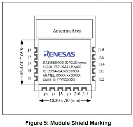
Note that J1 has no internal connection. J1 should be connected to ground.
Table 1: Pin Description
| Pin # | Pin Name | Type | Reset State | Description |
| J1 | n.c | Not internally connected. Recommended to be connected to ground externally | ||
| J2 | GND | GND | Ground | |
| J3 | GND | GND | Ground | |
| J4 | GND | GND | Ground | |
| J5 | P0_6 | DIO
(Type A) Note 1 |
I-PD | INPUT/OUTPUT with selectable pull- up/down resistors. Pull-down enabled during and after reset. General purpose I/O port bit or alternate function nodes. Contains a state retention mechanism during power down |
| J6 | GND | GND | Ground | |
| J7 | VBAT | PWR | POWER. Battery connection. IO supply | |
| J8 | P0_11 | DIO | I-PD | INPUT/OUTPUT with selectable pull- |
| (Type A) | up/down resistors. Pull-down enabled during and after reset. General purpose I/O port bit or alternate function nodes. Contains a state retention mechanism during power down | |||
| J9 | P0_10 | DIO (Type A) | I-PD | INPUT/OUTPUT with selectable pull- up/down resistors. Pull-down enabled during and after reset. General purpose I/O port bit or alternate function nodes. Contains a state retention mechanism during power down |
| SWDIO | INPUT/OUTPUT. SWI Data input/output. Bidirectional data and control communication (by default) | |||
| J10 | P0_2 | DIO
(Type B) |
I-PD | INPUT/OUTPUT with selectable pull- up/down resistors. Pull-down enabled during and after reset. General purpose I/O port bit or alternate function nodes. Contains a state retention mechanism during power-down |
| SWCLK | INPUT SWI clock signal (by default) | |||
| J11 | GND | GND | Ground | |
| J12 | P0_0 | DIO
(Type B) Note 2 |
I-PD | INPUT/OUTPUT with selectable pull- up/down resistors. Pull-down enabled during and after reset. General purpose I/O port bit or alternate function nodes. Contains a state retention mechanism during power-down |
| RST | RST active high hardware reset (default) | |||
| J13 | P0_7 | DIO
(Type A) |
I-PD | INPUT/OUTPUT with selectable pull- up/down resistors. Pull-down enabled during and after reset. General purpose I/O port bit or alternate function nodes. Contains a state retention mechanism during power down |
| J14 | P0_5 | DIO
(Type B) |
I-PD | INPUT/OUTPUT with selectable pull- up/down resistors. Pull-down enabled during and after reset. General purpose I/O port bit or alternate function nodes. Contains a state retention mechanism during power down |
| J15 | P0_9 | DIO
(Type A) |
I-PD | INPUT/OUTPUT with selectable pull- up/down resistors. Pull-down enabled during and after reset. General purpose I/O port bit or alternate function nodes. Contains a state retention mechanism during power down |
| J16 | P0_8 | DIO
(Type A) |
I-PD | INPUT/OUTPUT with selectable pull- up/down resistors. Pull-down enabled during and after reset. General purpose I/O port bit or alternate function nodes. Contains a state retention mechanism during power down |
Note 1
There are two types of pads, namely Type A and Type B. Type A is a normal IO pad with a Schmitt trigger on input while Type B has an extra RC Filter with a cutoff frequency of 100 kHz.
Note 2
This pin is also used for communication to the internal SPI FLASH.
- I-PD is Input-Pulled Down
- I-PU is Input-Pulled Up
- DIO is Digital Input-Output
- PWR is power
- GND is Ground
Characteristics
- All MIN/MAX specification limits are guaranteed by design, production testing, and/or statistical characterization. Typical values are based on characterization results at default measurement conditions and are informative only.
- Default measurement conditions (unless otherwise specified): VBAT= 3.0 V, TA = 25 oC. All radio measurements are done with standard RF measurement equipment.
Absolute Maximum Ratings
Stresses beyond those listed under Absolute Maximum Ratings may cause permanent damage to the device. These are stress ratings only, so functional operation of the device at these or any other conditions beyond those indicated in the operational sections of the specification are not implied. Exposure to Absolute Maximum Rating conditions for extended periods may affect device reliability.
Table 2: Absolute Maximum Ratings
| Parameter | Description | Conditions | Min | Max | Unit |
| VBAT_LIM | Limiting battery supply voltage | -0.2 | 3.6 | V |
Recommended Operating Conditions
Table 3: Recommended Operating Conditions
| Parameter | Description | Conditions | Min | Typ | Max | Unit |
|
VBAT |
Battery supply voltage enabling FLASH programming |
1.65 |
3.6 |
V |
||
|
VBAT_NOM |
Nominal battery supply voltage |
3 |
V |
|||
| VPIN | Voltage on a pin | -0.2 | 3.6 | V | ||
|
TA |
Ambient operating temperature |
-40 |
25 |
85 |
°C |
Device Characteristics
Table 4: DC Characteristics
| Parameter | Description | Conditions | Min | Typ | Max | Unit |
|
IBAT_ACTIVE |
Battery supply current with CPU running CoreMark from RAM at 16 MHz |
tbd |
mA |
|||
|
IBAT_BLE_ADV_ 100ms |
Average battery supply current with system in Advertising state (3 channels) every 100 ms and extended sleep with all RAM retained. TX output power at 3 dBm. FLASH is off. |
tbd |
μA |
|||
|
IBAT_BLE_CON |
Average battery supply current with system in a | tbd | μA |
|
N_30ms |
connection state with 30ms connection interval and extended sleep with all RAM retained. TX output power at 3 dBm. FLASH is off. | |||||
|
IBAT_FLASH |
Battery supply current with CPU fetching code from serial FLASH. RF is off. |
tbd |
mA |
|||
|
IBAT_HIBERN |
Battery supply current with system shut down (Hibernation or shipping mode). FLASH is off. |
tbd |
μA |
|||
|
IBAT_IDLE |
Battery supply current with CPU in Wait for Interrupt Mode. FLASH is off. |
tbd |
mA |
|||
|
IBAT_SLP_32KB |
Battery supply current with system in extended sleep mode and 32 kB RAM retained |
tbd |
μA |
|||
|
IBAT_SLP_64KB |
Battery supply current with system in extended sleep mode and all RAM retained |
tbd |
μA |
|||
|
IBAT_RF_RX |
Battery supply current |
Continuous RX; FLASH in sleep mode; DCDC converter is on; |
tbd |
mA |
||
|
IBAT_RF_TX_+3 dBm |
Battery supply current |
Continuous TX; FLASH in sleep mode; DCDC converter is on; Output power at 3 dBm; |
tbd |
mA |
||
|
IBAT_RF_TX_0d Bm |
Battery supply current |
Continuous TX;FLASH in sleep mode; DCDC converter is on; Output power at 0 dBm; |
tbd |
mA |
||
|
IBAT_RF_TX_- 3dBm |
Battery supply current |
Continuous TX;FLASH in sleep mode; DCDC converter is on; Output power at -3 dBm; |
tbd |
mA |
||
|
IBAT_RF_TX_- 7dBm |
Battery supply current |
Continuous TX;FLASH in sleep mode; DCDC converter is on; Output power at -7 dBm |
tbd |
mA |
||
|
IBAT_RF_TX_- 19dBm |
Battery supply current |
Continuous TX;FLASH in sleep mode; DCDC converter is on; Output power at -19.5 dBm |
tbd |
mA |
Table 5: XTAL32M – Recommended Operating Conditions
| Parameter | Description | Conditions | Min | Typ | Max | Unit |
| fXTAL(32M) | Crystal oscillator frequency | 32 | MHz | |||
|
ΔfXTAL(32M) |
Crystal frequency tolerance |
After optional trimming; including aging and temperature drift
Note 1 |
-20 |
20 |
ppm |
Note 1 Using the internal varicaps a wide range of crystals can be trimmed to the required tolerance.
Table 6: Digital I/O – Recommended Operating Conditions
| Parameter | Description | Conditions | Min | Typ | Max | Unit |
|
VIH |
HIGH level input voltage |
VDD=0.9V |
0.7*V DD |
V |
||
|
VIL |
LOW level input voltage |
VDD=0.9V |
0.3*V DD |
V |
Table 7: Digital I/O – DC Characteristics
| Parameter | Description | Conditions | Min | Typ | Max | Unit |
| IIH | HIGH level input current | VI=VBAT_HIGH=3.0V | -10 | 10 | μA | |
| IIL | LOW level input current | VI=VSS=0V | -10 | 10 | μA | |
| IIH_PD | HIGH level input current | VI=VBAT_HIGH=3.0V | 60 | 180 | μA | |
| IIL_PU | LOW level input current | VI=VSS=0V, VBAT_HIGH=3.0V | -180 | -60 | μA | |
|
VOH |
HIGH level output voltage |
IO=3.5mA, VBAT_HIGH=1.7V |
0.8*VB AT_HI GH |
V |
||
|
VOL |
LOW level output voltage |
IO=3.5mA, VBAT_HIGH=1.7V |
0.2*VB AT_HI GH |
V |
||
|
VOH_LOWDRV |
HIGH level output voltage |
IO=0.3mA, VBAT_HIGH=1.7V |
0.8*VB AT_HI GH |
V |
||
|
VOL_LOWDRV |
LOW level output voltage |
IO=0.3mA, VBAT_HIGH=1.7V |
0.2*VB AT_HI GH |
V |
Table 8: Radio – AC Characteristics
| Parameter | Description | Conditions | Min | Typ | Max | Unit |
| PSENS_CLEAN | sensitivity level | Dirty Transmitter disabled; | tbd | dBm |
| DC-DC converter disabled; PER = 30.8 %;
Note 1 |
||||||
|
PSENS_EPKT |
sensitivity level |
Extended packet size (255 octets) |
tbd |
dBm |
Note 1 Measured according to Bluetooth® Low Energy Test Specification RF-PHY.TS/4.0.1, section 6.4.1.
Mechanical Specifications
Dimensions
The module’s dimensions are shown in Figure 3.

PCB Footprint
The footprint for the PCB is shown in Figure 4.

Marking
Packaging Information
Tape and Reel

The actual reel specifications are presented in the following table:
Table 9: Reel Specifications
| Diameter | 13 inch |
| Reel tape width | 24 mm |
| Tape material | Antistatic |
| Qty/Reel | 100/1000 pcs |
| Leader | 400 mm + 10% |
| Trailer | 160 mm + 10% |
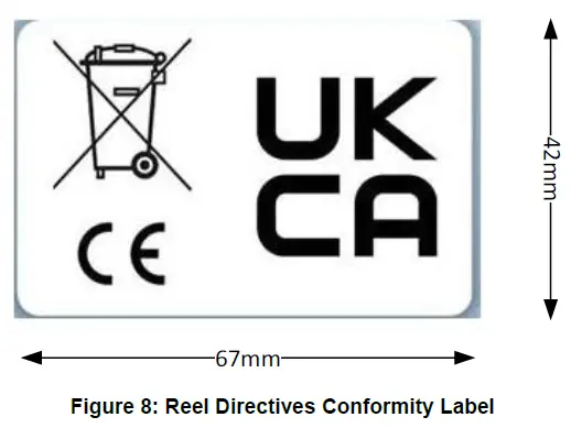
Labeling

The directives label shows information regarding directives conformity as in Figure 8.
Application Information
There are some special considerations for the use of the TINYTM module, namely:
- The RST signal is shared with the MOSI input of the NOR flash. For this reason, RST must not be driven to GND. When the internal Flash is in use, the reset functionality is not available
- The SPI Bus of DA14535 is used for the communication of the SoC with the NOR Flash at boot time. Three of the four signals are not driven to external module pins. For this reason, a sensor that utilizes the SPI bus must be assigned (by software) to the module pins to communicate with after the boot is completed and when NOR Flash is no longer in use. An example is given in Figure 12.

Note that the P0_0/RST pin (J12) should not be driven while the TINYTM module boots from its internal SPI FLASH.
Design Guidelines
- The DA14535 SmartBond TINY™ Module comes with an integrated PCB trace antenna. The antenna area is 12×4 mm. The antenna’s Voltage Standing Wave Ratio (VSWR) and efficiency depend on the installation location.
- The radiation performance of the PCB trace antenna depends on the host PCB layout. The maximum antenna gain is -0.5 dBi when installed on a 50×50 mm reference board, as shown in Figure 21. The radiation pattern is omnidirectional.
- The RF front end is optimized to achieve the maximum possible efficiency for various installation positions of the module on a host PCB. To obtain a similar performance, follow the guidelines described in the following sections.
Installation Location
- For optimum performance, install the module at the edge of a host PCB with the antenna edge facing out. The module can be located on either of the outer corners or the middle of the host PCB with equivalent performance.
- The antenna should have 4 mm free space in all directions. Copper or laminate in the proximity of the PCB trace antenna will affect the efficiency of the antenna. Laminate or copper under the antenna should be avoided as it severely affects the performance of the antenna. The antenna keep-out area can be seen in Figure 11.
- Metals close to the antenna will degrade the antenna’s performance. The amount of degradation depends on the host system’s characteristics.
- Table 10 summarizes the antenna efficiency at different installation locations on a host PCB as shown in Figure 10.
Table 10: Antenna Efficiency vs TINYTM Module Positions
| Position # 1 (Left) | Position # 2 (Middle) | Position # 3 (Right) | ||||
| Freq | Antenna efficiency | Antenna efficiency | Antenna efficiency | |||
| [MHz] | [%] | [dB] | [%] | [dB] | [%] | [dB] |
| 2405 | 52 | -2,8 | 40 | -4,0 | 40 | -4,0 |
| 2440 | 46 | -3,4 | 34 | -4,7 | 41 | -3,9 |
| 2480 | 50 | -3,0 | 40 | -4,0 | 52 | -2,8 |


The actual TINYTM module evaluation board layout that has been used to conduct measurements is shown in Figure 12.

Antenna Graphs
The antenna VSWR measurements for the three installation positions are shown in the following figures.

Radiation Pattern
The antenna radiation pattern measurements are carried out in an anechoic chamber. Radiation patterns are presented for three measurement planes: XY-, XZ-, and YZ- planes with horizontal and vertical polarization of the receiving antenna.
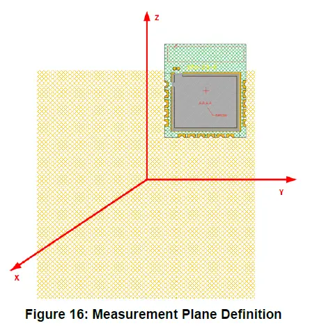
Measurements are carried out for the module installed in the upper right corner of the reference board with no laminate below the antenna trace.

Soldering
- The successful reflow soldering of the DA14535 TINYTM Module on a PCB depends on several parameters such as the thickness of the stencil, the pads solder paste aperture, the solder paste characteristics, the reflow soldering profile, size of the PCB, and so on.
- The volume of solder paste applied to the board is mainly determined by the aperture size and stencil thickness. An initial solder paste aperture for the pads is provided on the solder paste layer of the PCB footprint. This aperture is modified by the assembly process experts according to stencil thickness, solder paste, and available assembly equipment.
- The solder profile depends on the solder paste type used. For example, the soldering profile of a lead-free solder paste, Sn3Ag0.5Cu with no clean Flux (ROL0) and Solder Powder Type 4, is presented below.
- No clean flux is recommended because washing must not be applied after assembly to avoid moisture being trapped under the shield.

Table 11: Reflow Profile Specification
| Statistic Name | Low Limit | High Limit | Units |
| Slope1 (Target=2.0) Between 30.0 and 70.0 | 1 | 3 | Degrees/Second |
| Slope2 (Target=2.0) Between 70.0 and 150.0 | 1 | 3 | Degrees/Second |
| Slope3 (Target=-2.8) Between 220.0 and 150.0 | -5 | -0.5 | Degrees/Second |
| Preheat time 110-190°C | 60 | 120 | Seconds |
| Time above reflow @220°C | 30 | 65 | Seconds |
| Peak temperature | 235 | 250 | Degrees Celsius |
| Total time above @235°C | 10 | 30 | Second |
Solderability reflow check of five cycles was performed, applying the procedures mentioned in the JESD-A113E standard. The MSL is an indicator for the maximum allowable time period (floor lifetime) in which a moisture-sensitive plastic device, once removed from the dry bag, can be exposed to an environment with a maximum temperature of 30 °C and a maximum relative humidity of 60 % RH before the solder reflow process.
- DA14535 TINY Module is qualified for MSL 3.
Table 12: MSL Level vs Floor Lifetime
| MSL Level | Floor Lifetime |
| MSL 4 | 72 hours |
| MSL 3 | 168 hours |
| MSL 2A | 4 weeks |
| MSL 2 | 1 year |
| MSL 1 | Unlimited at 30 °C/85 %RH |
Ordering Information
The ordering number consists of the part number followed by a suffix that indicates the packing method. For details and availability, consult your Renesas local sales representative.
Table 13: Ordering Information (Samples)
| Part Number | Size (mm) | Shipment Form | Pack Quantity | MOQ |
| DA14535MOD- 00F0100C | 12.5
x 14.5 x 2.8 |
Reel | 100 | 3 |
Table 14: Ordering Information (Production)
| Part Number | Size (mm) | Shipment Form | Pack Quantity | MOQ |
| DA14535MOD- 00F01002 | 12.5 x
14.5 x 2.8 |
Reel | 1000 | 1 |
Regulatory Information
This section outlines the regulatory information for the DA14535 SmartBond TINYTM Module. The module is certified for the global market. This facilitates the market entry of the end product. Note that the end product would need to apply for the end product certification, however, the module certification listed below will facilitate that procedure.
When the user sends the end product to those markets, the end product may need to follow additional requirements according to the specific market regulation. For example, some markets have additional testing and/or certification like Korea EMC, South Africa SABS EMC and some have the requirement to put on the end product label a modular approval ID or mark that consists of an approved Bluetooth® Low Energy modular ID on host label directly, like Japan, Taiwan, Brazil.
A list of the Conformance Standards that the DA14535 SmartBond TINYTM Module meets is shown in Table 15.
Table 15: Standards Conformance
| Area | Item | Service | Standard | Certificate ID |
|
Global |
Safety for module |
CB |
IEC 62368-1:2018 |
CERTIFICATION IN PROGRESS
Note 1 |
|
Europe |
Wireless |
RED |
EN 300 328 v2.2.2
EN 62479:2010 |
CERTIFICATION IN PROGRESS |
| Safety for module | CE | EN IEC 62368-1:
2020+A11: 2020 |
||
|
EMC |
RED |
EN 301 489-1 v2.2.3
EN 301 489-17 v3.2.4 |
||
|
UK |
Wireless |
UKCA-RED |
EN 300 328 v2.2.2
EN 62479:2010 |
CERTIFICATION IN PROGRESS |
| Safety for module | UKCA-LVD | BS EN IEC 62368- 1: 2020+A11: 2020 | ||
|
EMC |
UKCA-RED |
EN 301 489-1 V2.2.3
EN 301 489-17 V3.2.4 |
||
|
US/CA |
Wireless |
FCC ID |
47 CFR PART 15
Subpart C: 2021 section 15.247 |
Y82-DA14535MOD |
|
IC ID |
RSS-247 Issue 2:
February 2017 RSS-Gen Issue 5: April 2018+A1: March 2019+A2: February 2021 |
9576A-DA14535MOD |
||
| Japan | Wireless | MIC | JRL | 012-230026 |
| Taiwan | Wireless | NCC | LP0002 | CERTIFICATION IN PROGRESS |
|
South Korea |
Wireless |
MSIP |
방송통신표준
KS X 3123 “무선 설비 적합성 평가 시험 방법” KN 301 489 |
R-R-8DL-DA14535MOD |
| South Africa | Wireless | ICASA | Based on RED | CERTIFICATION IN PROGRESS |
|
Brazil |
Wireless |
Anatel |
ATO No.14448/2017
Resolution No.680 |
CERTIFICATION IN PROGRESS |
| China | Wireless | SRRC | 信部无【2002】353 | CERTIFICATION IN PROGRESS |
| Thailand | Wireless | NBTC | NBTC TS 1035-
2562 |
CERTIFICATION IN PROGRESS |
| India | Wireless | WPC | Based on RED | CERTIFICATION IN PROGRESS |
| Australia/ New Zealand | Wireless | ACMA | Based on RED | CERTIFICATION IN PROGRESS |
Note 1
Include national differences of the US/Canada/Japan/China/Korea/Europe/Australia/South Africa/Taiwan/Brazil/Thailand.
CE (Radio Equipment Directive 2014/53/EU (RED)) – (Europe)
The DA14535 SmartBond TINYTM Module is a Radio Equipment Directive (RED) assessed radio that is CE marked. The module has been manufactured and tested with the intention of being a subassembly to a final product. The module has been tested to RED 2014/53/EU Essential Requirements for Health, Safety, and Radio. The applicable standards are:
- Radio: EN 300 328 V2.2.2 (2019-07)
- Health: (SAR) EN 62479:2010
- Safety: EN 62368-1
- EMC: EN 301 489-1 v2.2.3, EN 301 489-17 v3.2.4
End product will need to perform the radio EMC tests according to EN 301 489. The conducted tests can be inherited from the module test report. It is recommended to repeat the EN 300 328 radiated testing with the end product assembly.
FCC – (U.S.A.)
Model no. DA14535MOD-00F0100
FCC ID: Y82-DA14535MOD
List of Applicable FCC Rules
The module complies with FCC Part 15.247.
Summarize the Specific Operational Use Conditions
The module has been certified for Portable applications. This transmitter must not be co-located or operating in conjunction with any other antenna or transmitter.
Limited Module Procedures
- Not applicable.
Trace Antenna Designs
- Not applicable.
RF Exposure Considerations
This equipment complies with FCC’s RF radiation exposure limits set forth for an uncontrolled environment. The antenna(s) used for this transmitter must not be collocated or operating in conjunction with any other antenna or transmitter.
Antennas
| Type | Gain | Impedance | Application |
| PCB Antenna | -0.5 dBi | 50Ω | Fixed |
The antenna is permanently attached, can’t be replaced.
Label and Compliance Information
This device complies with part 15 of the FCC rules. Operation is subject to the following two conditions:
- This device may not cause harmful interference
Note 2 This device must accept any interference received, including interference that may cause undesired operation.
| Note |
| The manufacturer is not responsible for any radio or TV interference caused by unauthorized modifications or changes to this equipment. Such modifications or changes could void the user’s authority to operate the equipment. |
| Warning |
| Changes or modifications to this unit not expressly approved by the party responsible for compliance could void the user’s authority to operate the equipment. |
| Note |
| This equipment has been tested and found to comply with the limits for a Class B digital device, pursuant to part 15 of the FCC Rules. These limits are designed to provide reasonable protection against harmful interference in a residential installation. This equipment generates uses and can radiate radio frequency energy and, if not installed and used in accordance with the instructions, may cause harmful interference to radio communications. However, there is no guarantee that interference will not occur in a particular installation. If this equipment does cause harmful interference to radio or television reception, which can be determined by turning the equipment off and on, the user is encouraged to try to correct the interference by one or more of the following measures:
● Reorient or relocate the receiving antenna. ● Increase the separation between the equipment and receiver. ● Connect the equipment into an outlet on a circuit different from that to which the receiver is connected. ● Consult the dealer or an experienced radio/TV technician for help. |
The system integrator must place an exterior label on the outside of the final product housing the DA14535MOD-00F0100 Module. Below are the contents that must be included on this label.
OEM Labeling Requirements:
| Notice |
| The OEM must make sure that FCC labeling requirements are met. This includes a clearly visible exterior label on the outside of the final product housing that displays the contents shown in below: |
- Model: DA14535MOD-00F0100
- Contains FCC ID: Y82-DA14535MOD
Information on test modes and additional testing requirements:
When testing host product, the host manufacture should follow FCC KDB Publication 996369 D04 Module Integration Guide for testing the host products. The host manufacturer may operate their product during the measurements. In setting up the configurations, if the pairing and call box options for testing does not work, then the host product manufacturer should coordinate with the module manufacturer for access to test mode software.
Additional testing, Part 15 Subpart B disclaimer:
The modular transmitter is only FCC authorized for the specific rule parts (FCC Part 15.247) list on the grant, and that the host product manufacturer is responsible for compliance to any other FCC rules that apply to the host not covered by the modular transmitter grant of certification. The final host product still requires Part 15 Subpart B compliance testing with the modular transmitter installed when contains digital circuity.
IC (Canada)
- Model no. DA14535MOD-00F0100
- IC ID: 9576A-DA14535MOD
The DA14535 SmartBond TINYTM Module is certified for the IC as a single-modular transmitter. The module meets IC modular approval and labeling requirements. The IC follows the same testing and rules as the FCC regarding certified modules in authorized equipment.
The module has been tested according to the following standards:
- Radio: RSS-247 Issue 2: February 2017, RSS-Gen Issue 5: April 2018+A1: March 2019+A2: February 2021
- Health: RSS-102 Issue 5:2015
This device contains licence-exempt transmitter(s)/receiver(s) that comply with Innovation, Science and Economic Development Canada’s license-exempt RSS(s). Operation is subject to the following two conditions:
- This device may not cause interference.
- This device must accept any interference, including interference that may cause undesired operation of the device.
RF Exposure Statement
This device complies with IC radiation exposure limits set forth for an uncontrolled environment and meets RSS-102 of the IC radio frequency (RF) Exposure rules. This transmitter must not be co-located or operating in conjunction with any other antenna or transmitter.
OEM Responsibilities to comply with IC Regulations
OEM integrator is responsible for testing their end product for any additional compliance requirements needed for the module installation like IC ES003 (EMC). This can be combined with the FCC Part 15B test.
End product labeling
The DA14535 SmartBond TINYTM Module is labeled with its own IC ID: 9576A-DA14535MOD. If the IC ID is not visible when the module is installed inside another device, then the host product must be labelled to display the ISED certification number for the module, preceded by the word “contains” or similar wording expressing the same meaning, as follows: Contains IC: 9576A-DA14535MOD.”
UKCA (UK)
UKCA ID: CERTIFICATION PENDING
The module has been tested and found to comply with the standards harmonized with the regulations listed below according to UKCA-Radio Equipment Regulations 2017-CHAPTER 1 6(1)(a) Health, 6(1)(b) & 6(2).
The applicable standards are:
- Radio: EN 300 328 V2.2.2 (2019-07)
- Health: (SAR) EN 62479:2010
- Safety: EN 62368-1:2018, BS EN IEC 62368-1: 2020+A11: 2020
- EMC: EN 301 489-1 v2.2.3, EN 301 489-17 v3.2.4
End-product will need to perform the radio EMC tests according to EN 301 489. The conducted tests can be inherited from the module test report. It is recommended to repeat the EN 300 328 radiated testing with the end product assembly.

NCC (Taiwan)
NCC ID: CERTIFICATION PENDING
![]()
The DA14535 SmartBond TINYTM Module has received compliance approval in accordance with the Telecommunications Act. The module has been tested according to the following standard:
- Radio: Low Power Radio Frequency Devices Technical Regulations (LP0002)
End product may need to follow additional requirements according to the regulation EMC.
End product labeling
The NCC ID can be applied directly to the end product’s label.
MSIP (South Korea)
- Model no. DA14535MOD-00F0100
- MSIP ID: R-R-8DL-DA14535MOD
DA14535 SmartBond TINYTM Module has received certification of conformity in accordance with Radio Waves Act. The module has been tested according to the following standard:
- Radio: Ministry of Science and ICT Notice No. 2019-105
For the end product wireless test, you can refer to Renesas’ own certification report so that the lab knows the module itself has passed although it still needs to be tested.
- Additionally, EMC for wireless (KN301489).
End product labeling
The MSIP ID can be applied directly to the end product’s label. The ID should be clearly visible on the final end product. The integrator of the module should refer to the labeling requirements for Korea available on the Korea Communications Commission (KCC) website.
ICASA (South Africa)
South Africa certification is based on RED(CE) approval.

Approval is granted to print labels for the products as described below:
- For use as Label on the product size: 80 mm (W) X 40 mm (H). To be printed on the product.
- For use as Label on the package size: 80 mm (W) X 40 mm (H). To be printed on the package.
End product may need to follow additional requirements according to the regulation EMC.
ANATEL (Brazil)
- Model no. DA14535MOD-00F0100
- ANATEL ID: CERTIFICATION PENDING

The module has been tested and found to be compliant according to the following Category II standards:
- ATO (Act) No 14448/2017
End product may need to follow additional requirements according to the regulation EMC.
“Este equipamento não tem direito à proteção contra interferência prejudicial e não pode causar interferência em sistemas devidamente autorizados.
Translation of the text:
“This equipment is not entitled to protection against harmful interference and must not cause interference in duly authorized systems.”
SRRC (China)
Model no. DA14535MOD-00F0100
- CMIIT ID: CERTIFICATION PENDING
The module has been tested and found to be compliant according to the following standards:
End product may need to follow additional requirements according to the regulation EMC.
MIC (Japan)
- Model no. DA14535MOD-00F0100
- MIC ID: 012-230026

The DA14535 SmartBond TINYTM Module has received type certification as required to conform to the technical standards regulated by the Ministry of Internal Affairs and Communications (MIC) of Japan pursuant to the Radio Act of Japan.
The module has been tested according to the following standard:
- Radio: JRL “Article 49-20 and the relevant articles of the Ordinance Regulating Radio” Equipment End product may need to follow additional requirements according to the regulation EMC.
End product labeling
The MIC ID can be applied directly to the end product’s label. The end product may bear the GITEKI mark and certification number so that is clear that the end product contains a certified radio module. The following note may be shown next to, below, or above the GITEKI mark and certification number in order to indicate the presence of a certified radio module:
SmartBond TINY Bluetooth® LE Module
Translation of the text:
“This equipment contains specified radio equipment that has been certified to the Technical Regulation Conformity Certification under the Radio Law.”
NBTC (Thailand)
- Model no. DA14535MOD-00F0100
- NBTC SDoC ID: CERTIFICATION PENDING
- The DA14535 SmartBond TINYTM Module is compliant with NBTC requirements in Thailand.
- End product may need to follow additional requirements according to the regulation EMC.
End product labeling
End products will have their own ID and labeling requirements.
WPC (India)
- Model no. DA14535MOD-00F0100
- Registration No: CERTIFICATION PENDING
- India certification is based on RED(CE) approval/reports. There are no marking/labeling requirements.
- End product may need to follow additional requirements according to the regulation EMC.
Australia/ New Zealand
- Model no. DA14535MOD-00F0100
- Registration No: CERTIFICATION PENDING
Revision History
| Revision | Date | Description |
| 1.0 | 22-Jun-2023 | First release. |
| 1.1 | 09-Aug-2023 | Updated Key Features with maximum output power. |
| 1.2 | 09-Sept-2023 | Updated with regulatory information |
| 1.3 | 22-Sept-2023 | Updated regulatory information |
| 1.4 | 26-Sept-2023 | Updated regulatory information |
| 1.5 | 28-Sept-2023 | Updated marking with FCC, IC ID |
Status Definitions
RoHS Compliance
Renesas Electronic’s suppliers certify that its products are in compliance with the requirements of Directive 2011/65/EU of the European Parliament on the restriction of the use of certain hazardous substances in electrical and electronic equipment. RoHS certificates from our suppliers are available on request.
Important Notice and Disclaimer
RENESAS ELECTRONICS CORPORATION AND ITS SUBSIDIARIES (“RENESAS”) PROVIDES TECHNICAL SPECIFICATIONS AND RELIABILITY DATA (INCLUDING DATASHEETS), DESIGN RESOURCES (INCLUDING REFERENCE DESIGNS), APPLICATION OR OTHER DESIGN ADVICE, WEB TOOLS, SAFETY INFORMATION, AND OTHER RESOURCES “AS IS” AND WITH ALL FAULTS, AND DISCLAIMS ALL WARRANTIES, EXPRESS OR IMPLIED, INCLUDING, WITHOUT LIMITATION, ANY IMPLIED WARRANTIES OF MERCHANTABILITY, FITNESS FOR A PARTICULAR PURPOSE, OR NON-INFRINGEMENT OF THIRD PARTY INTELLECTUAL PROPERTY RIGHTS.
These resources are intended for developers skilled in the art of designing with Renesas products. You are solely responsible for (1) selecting the appropriate products for your application, (2) designing, validating, and testing your application, and (3) ensuring your application meets applicable standards, and any other safety, security, or other requirements. These resources are subject to change without notice. Renesas grants you permission to use these resources only for the development of an application that uses Renesas products. Other reproduction or use of these resources is strictly prohibited. No license is granted to any other Renesas intellectual property or to any third party intellectual property. Renesas disclaims responsibility for, and you will fully indemnify Renesas and its representatives against, any claims, damages, costs, losses, or liabilities arising out of your use of these resources. Renesas’ products are provided only subject to Renesas’ Terms and Conditions of Sale or other applicable terms agreed to in writing. No use of any Renesas resources expands or otherwise alters any applicable warranties or warranty disclaimers for these products.
© 2023 Renesas Electronics Corporation. All rights reserved.
Corporate Headquarters
- TOYOSU FORESIA, 3-2-24 Toyosu Koto-ku, Tokyo 135-0061, Japan
- www.renesas.com
Trademarks
Renesas and the Renesas logo are trademarks of Renesas Electronics Corporation. All trademarks and registered trademarks are the property of their respective owners.
Contact Information
For further information on a product, technology, the most up-to-date version of a document, or your nearest sales office, please visit: https://www.renesas.com/contact/.
© 2023 Renesas Electronics.
Documents / Resources
 |
RENESAS DA14535MOD SmartBond TINY Bluetooth LE Module [pdf] User Manual DA14535MOD SmartBond TINY Bluetooth LE Module, DA14535MOD, SmartBond TINY Bluetooth LE Module, TINY Bluetooth LE Module, Bluetooth LE Module, LE Module |


