RENESAS RA family, RX family 32-Bit Arm Cortex-M Microcontrollers Owner’s Manual

Summary
This guideline is intended to help those who are familiar with QFP (Quad Flat Package) and who are planning to use BGA (Ball Grid Array) packages for the first time. This document is a summary of points to note when designing a board that uses a BGA package.
Target Device
RA family, RX family
Characteristic of BGA packaging
What is BGA packaging
BGA package refers to a package in which solder balls are mounted on the back of the package (see Figure 1). BGA has the following characteristics compared to QFP.
Features of BGA package compared to QFP:
– A BGA package is typically smaller than an LQFP for the same number of pins.
– A BGA package typically has more pins than an LQFP for the same package size.
– BGA packages are better for heat dissipation as they have lower thermal resistance than QFP packages as there is a better heat dissipation path through the substrate.
– BGA packages are better low impedance and high transmission speeds because the package length can be shortened by miniaturization and the substrate (interposer) can be multilayered.
– BGA packages have an optimal ball arrangement when electrical characteristics are considered. However, if it is not necessary to consider the electrical characteristics, the ball can be placed anywhere.
Note: BGA with a plastic package material is called PBGA (Plastic BGA). In Renesas, BGA generally refers to PBGA.
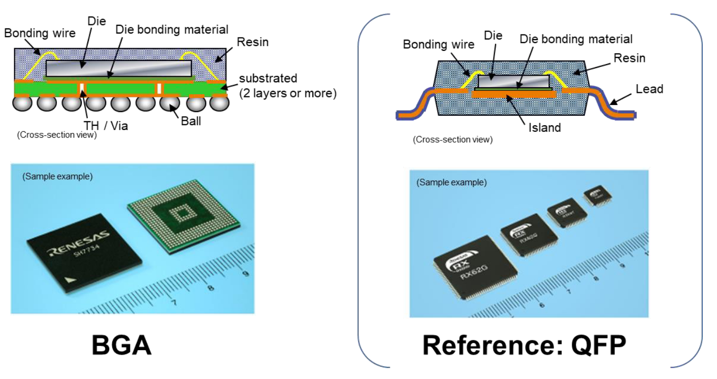
Figure 1, Cross-section view of BGA package and QFP and sample examples
Example of BGA ball arrangement
As shown in Figure 2, the number of signals that can be connected to QFP is almost fixed relative to the package size (See Figure 2, Case QFP), BGA packages can be roughly divided into three ball arrangements.
– The first is when the ball is placed on the outer periphery of the package (See Figure 2, Case BGA①). It is used when the number of signals is relatively small for the package size.
– The second is when a thermal ball is placed directly under the chip in addition to the outer circumference of the package (See Figure 2, Case BGA②). It is adopted when heat dissipation needs to be considered.
– The third is when the balls are placed across the entire surface of the package without gaps (See Figure 2, Case BGA③). It is used when the number of signals is large. In general, it is more difficult to design packages and boards with such a package, and both the package and the board it can be mounted on can become expensive.

Definition of BGA, FBGA and LGA
As shown in Figure 3, BGA and FBGA (Fine Pitch Ball Grid Array) have different terminal pitch specifications. A package with a terminal pitch of 1 mm or more is called BGA, and a package with a terminal pitch of 0.8 mm or less is called FBGA.

Figure 3, Definition of BGA and FBGA
As shown in Figure 4, BGA and LGA (Land Grid Array) differ in the presence or absence of solder ball terminals. A package with solder ball terminals is called BGA, and a package without solder ball terminals is called LGA.

Figure 4, Definition of BGA and LGA
Package name and code (JEITA code)
The package of our ICs is uniformly assigned a JEITA package code in accordance with the JEITA standard “EIAJ ED-7303C”. The structure of the JEITA package code is introduced below.
The package code consists of the following 6 items and is displayed in a maximum of 30 characters.

Package body material code:(1)
- The package body material code is displayed as a single character according to the classification in Table
Table 1, Package body material code

Package Appearance Feature Codes:(2)
The package appearance feature code is displayed in up to 3 characters as necessary according to the functional classification in Table 2.
Table 2, Package Appearance Feature Codes

Basic package name code:(3)
The basic package name code is displayed in three characters in principle according to the basic package name. The form classification of the package conforms to EIAJ ED-7300. As an exception, only the derived package name codes TSOP (1), TSOP (2), DTP (1), and DTP (2) corresponding to the basic package name code SOP and DTP are treated as basic package name codes, and 7 or 6 characters are allowed. At this time, TSOP (1) and TSOP (2) do not use conventional TSOP (I), TSOP (II), or the like. Further, in the case of TSOP (1), TSOP (2), DTP (1), and DTP (2), when the maximum number of digits of the package code exceeds 30 digits, the number of package terminals is omitted as shown in the example.
Package Terminal Number Codes:(4)
The number of terminal codes in the package is displayed in a maximum of 5 characters. The terminal is a general term for electrodes with different external connection methods, such as leads, pins, lands, bumps, and balls. Medium nuke indication is allowed for less than 100 pins, and 5 characters are specified. For example, in the case of a 28-pin package with 2 medium nukes, it is written as 28/26.
Package Nominal Dimension Codes:(5)
As shown in the example, the package nominal dimension code consists of “package body width (mm)” × “package body length (mm)” and is displayed in a maximum of 11 characters. However, if the decimal number is “x0” or “00”, “0” and “00” are not noted.
Terminal Linear Spacing Codes:(6)
The terminal linear spacing code is displayed in 4 characters. Terminal linear spacing in inches (inches) in millimeters (mm) is rounded according to ISO R370.
Properties of BGA Packaging
Thermal resistance(A value that expresses the difficulty of transmitting temperature)
Compared to QFP, BGA has the advantage of low thermal resistance because it increases the heat dissipation path through the substrate. In other words, BGAs have better heat dissipation characteristics than QFP (See Figure 5).
As shown in Figure 5, compared to QFP, BGA has lower thermal resistance than QFP because in addition to the heat dissipation path from the lead portion and resin indicated by the red arrow, the heat generated by the chip indicated by the purple arrow is dissipated from directly under the chip from the source of heat generation through vias and balls of the package.

Electrical characteristics
BGA packages can be made smaller than packages with pins such as QFP packages, which is better for low impedance and high transmission speed (See Figure 6).
– Compared to QFP packages, BGA can shorten the total length inside the package, so that the inductance and resistance components can be lowered.
– The bonding-wire length and trace length inside a BGA package can be further shortened, and the inductance and resistance components can be lowered by reducing the package size of BGA.
Example: Since the BGA can reduce the power supply impedance, it is possible to reduce the number of bypass capacitors (hereinafter referred to as CC: Chip Capacitor) in the power supply and contribute to the reduction of BOM cost.

Figure 6, Image of BGA package total length (compared with QFP) and electrical characteristics
Implementation of BGA packaging
RA/RX BGA lineup of microcontrollers
RA/RX microcontrollers offer the following packages mainly for small consumer devices (See Figure 7 and Table 3).

Figure 7, RA/RX BGA lineup of microcontrollers
Table 3, List of BGA lineup of RA/RX microcontrollers

Recommended board design rules with through hole (TH)
The recommended board design rules for boards using TH are shown below (See Figure 8). In order to maximize the benefits of BGA packages in terms of traces and characteristics, it is recommended to apply board design rules that allow trace to pass between balls. It is recommended that the trace width in the package mounting area be at least 100 um.
Note: The recommended rules may vary depending on the board manufacturer, and it is necessary to contact the board manufacturer for details.

Figure 8, Recommended board design rules with through hole
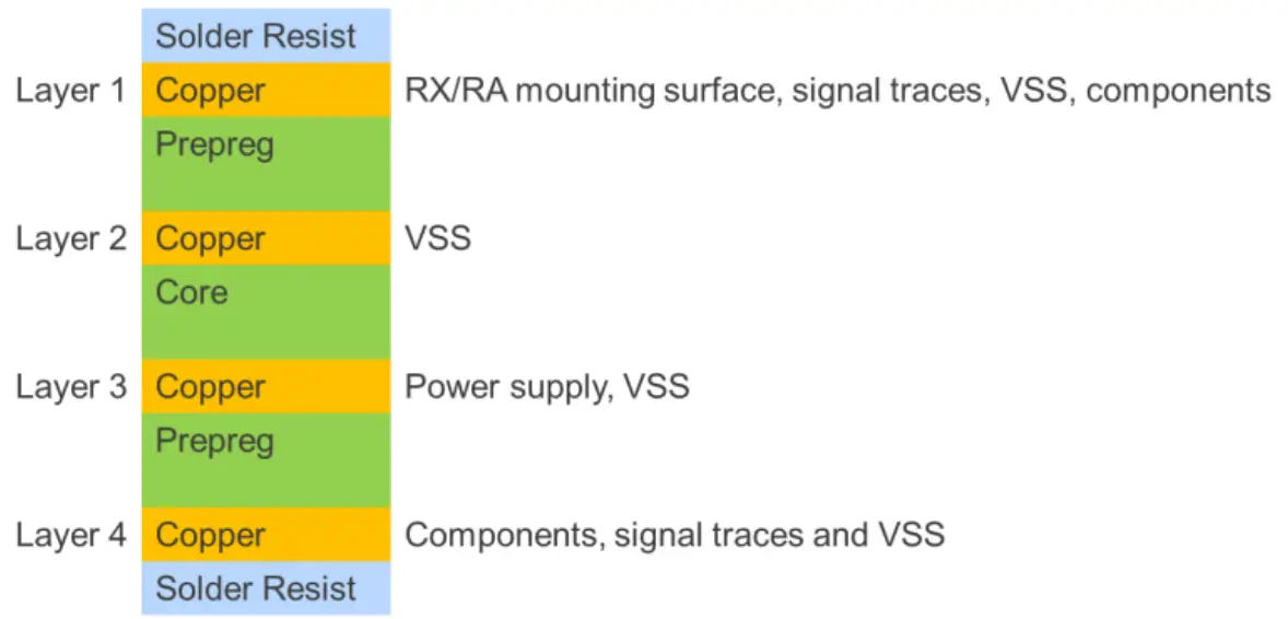
Recommended layer configuration
As for the layer configuration of the board, a 4-layer board is recommended (See Figure 9). It is recommended that the RA/RA microcontroller should be placed on Layer 1 along with the with signal trace, VSS, and other components, VSS planes should be routed on layer 2, the minimum necessary power supply plane and VSS plane should be routed on Layer 3, and with components, signal traces, and VSS on Layer 4. If it is necessary to further improve the electrical characteristics, it is recommended to add an additional two layers between the layer 2 and layer 3.
Basic board design concept
The basic idea of board design can be roughly divided into two steps. The 1st step (①) in which the outer circumference 2 Row is wired with a surface layer (Layer 1) where the RA/RX is mounted , and a 2nd step (②) in which the inner circumference 2 Row is wired on the back side (Layer 4) or an inner layer (2 or 3 layer) that is opposite the layer where the RA/RX through TH.
Figure 10 is an example of the layout of the basic concept of Layer 1 and Layer 4 of a full grid 64 BGA, and Figure 11 is a layout example of the basic concept of Layer 1 and Layer 4 of the outer circumference 4 Row-144 BGA. The red wire indicates the trace of Layer 1, the black circle indicates the ball, and the green wire and the green circle indicate the lead out line from the ball and TH. This example shows a case where one wire passes between the balls. If the trace does not pass between the balls, the trace layer increases by one, and depending on the trace situation of the other layers, the number of substrate layers may be 6 or more. The gray dotted circle indicates the ball passing through Layer 1, and the green circle indicates the TH and the callout line from TH. Although not shown, the capacitor is placed near TH. In addition, the TH position and trace withdrawal direction change depending on the specifications of the microcomputer mounted circuit.

Figure 10, Example of basic layout for Layer 1 and Layer 4 of a 64 (8×8) BGA full grid (Top View)
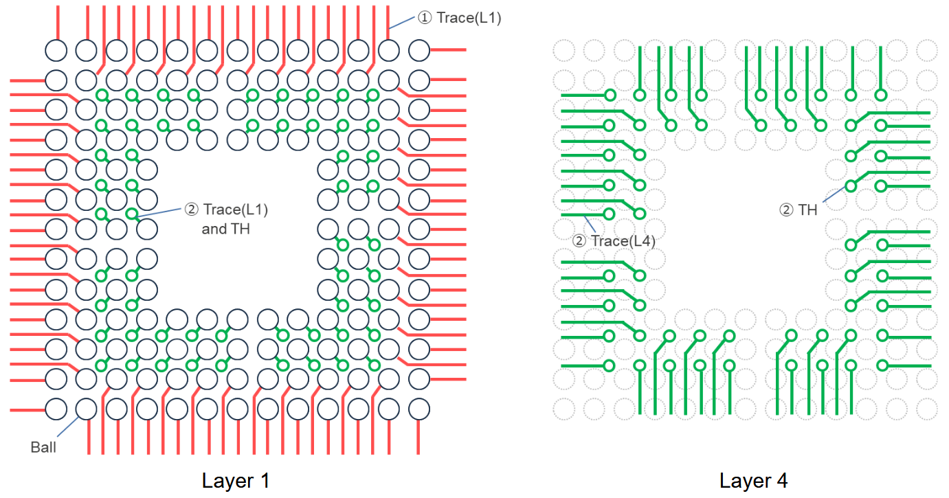
Figure 11, Example of basic layout for L1 and L 4 of 144(13×13)BGA outer perimeter 4 rows (Top View)
Recommended board design rules
Power Supply, VCL
– Connect a capacitor (a ceramic capacitor with good frequency characteristics) to the power supply pin with the shortest possible distance between the paired VSS. A capacitor is placed close to the IC/package and connected to the common plane after the capacitor (See Figure 12). The current is designed to flow through the IC/package, through the capacitors, and through the common power supply VSS plane in order (See Figure 13).
-,It is recommended that the capacitor is mounted on the same side as the IC/package when the power supply terminals are arranged in the outer circumference 2row, and on the opposite side (back side/Layer 4) from the IC/package when the power supply terminals are arranged in the 3row or later.
– If there are specifications such as the distance from the IC/package to the capacitor (resistance/inductance value of trace and THs), capacitor capacitance and insertion position, ferrite bead insertion position, merge position with other power supplies, etc., follow each specification.
– The trace width and the number of THs after passing through the capacitor should take into account the size of the current that could flow, and design the trace with a width and a TH that exceeds the required number. Separate these traces as much as possible from other power supply balls to reduce the amount of coupling (including adjacent layers).
– Shield with VSS as much as possible. If VSS shielding is not possible, increase the spacing (>2×h (thickness between adjacent layers)).

Figure 12, Image of recommended capacitor design for power supply and VCL (Layer 1 and 4, Top View)

Figure 13, Recommended capacitor design image for Power Supply and VCL
Reset
– When connecting directly to the reset IC, place the reset IC as close to the microcontroller as possible (See Figure 14).
– When suppressing noise, it is recommended to insert a low-pass filter. (VSS shielding is not required when inserting a low-pass filter.) (See Figure 14)
– Keep a distance from other signals (especially traces with large currents and high-speed signal traces), and shield them with a VSS that is wide and has multiple THs (See Figure 14).

Figure 14, Recommended Design Image for Reset (Top View)
Clock
– The traces for Clock input/output terminals such as EXATL, XTAL, XCIN, XOUT, X1, X2, etc. should be as short as possible, including peripheral circuits.
– Separate these from other traces (especially traces with large currents and high-speed signals) and shield them with VSS.
– The width of the VSS shield traces should be 0.3 mm or more, and the distance between the VSS shield traces and the clock traces should be 0.3~2 mm.
– The layer below the peripheral circuit of the crystal does not allow the trace of signals, power supplies, or VSS patterns (See Figure 15).
OSC
– For external components (capacitors, resistors, etc.) when using a quartz crystal, select the most suitable components for the crystal to be used.
– The power supply shall comply with the recommended rules for board design in Section 3.5.1.
– OSC signal trace is wired with a trace width of 0.1 mm on the microcontroller mounting surface, and VSS shielding is performed at the same layer and the bottom layer. There is nothing in the middle layer, including other signals. A distance of 0.3 mm should be maintained between OSC signal traces in the same layer and other signal traces (especially traces with large currents and high-speed signal patterns) and VSS shields. (See Figure 15)
– Place the crystal as close as possible to the terminals (within 10 mm). (See Figure 15)

Figure 15, Recommended design image of OSC
USB
– The power supply shall comply with the recommended rules for board design in Section 3.5.1. However, the USB VSS is separated from the others and shorted at one point.
– The RREF resistor is placed in the vicinity of the IC/package, but not in parallel with the capacitor.
– Trace including RREF resistors is shielded with USBAVSS across the same layer and adjacent layers. If it cannot be shielded, it should not be adjacent to other signals or paralleled. Do not cross as much as possible. Space out as much as possible.
– Differential signals (DP, DM) are designed with a differential impedance of 90 Ω ±10% and are wired in pairs (same length, parallel, same width, same number of bends, same number of THs). The approximate trace length difference is within 2 mm (See Figure 16). Shield with USB VSS. If it is not possible to shield, do not space it from other signals (especially traces with large currents or high-speed signal patterns) or parallel them. Do not cross as much as possible. Slots/slits in adjacent layers should also be avoided.

Figure 16, Recommended Design Diagram for Differential Signals
Analog
– The signal trace of the analog terminal is the same layer as the power supply/VSS/other signals (especially traces with large currents and high-speed signal patterns) with a Min trace width and /Space out adjacent layers, stop paralleling, and shield with analog VSS. The width of the analog VSS shield trace should be at least three times the width of the analog signal trace, and the distance between the analog signal trace and the analog VSS shield should be three times the trace width or three times that of the adjacent layers (See Figure 17).
– When inserting a low-pass filter, follow the specifications of the analog to be implemented.

Figure 17, Recommended design image: Example of shielded trace(Top View)
Example of board layout around BGA package
In accordance with the basic board layout concept in Section 3.4 and the recommended rules for board design in Section 3.5, examples of TH position and Layer 1 and Layer 4 layout that also take into account components placement (not shown) are shown in Figure 18 (example of RA6Mx/64BGA) and Figure 19 (example of RA6Mx/144BGA). For the power supply, it is recommended to consider the TH arrangement so that it is adjacent to the VSS so that the required number of capacitors can be mounted on the Layer 4 in the immediate vicinity of the ball. The magenta-colored circle in the figure is an example of a pair of TH of the power supply and VSS.
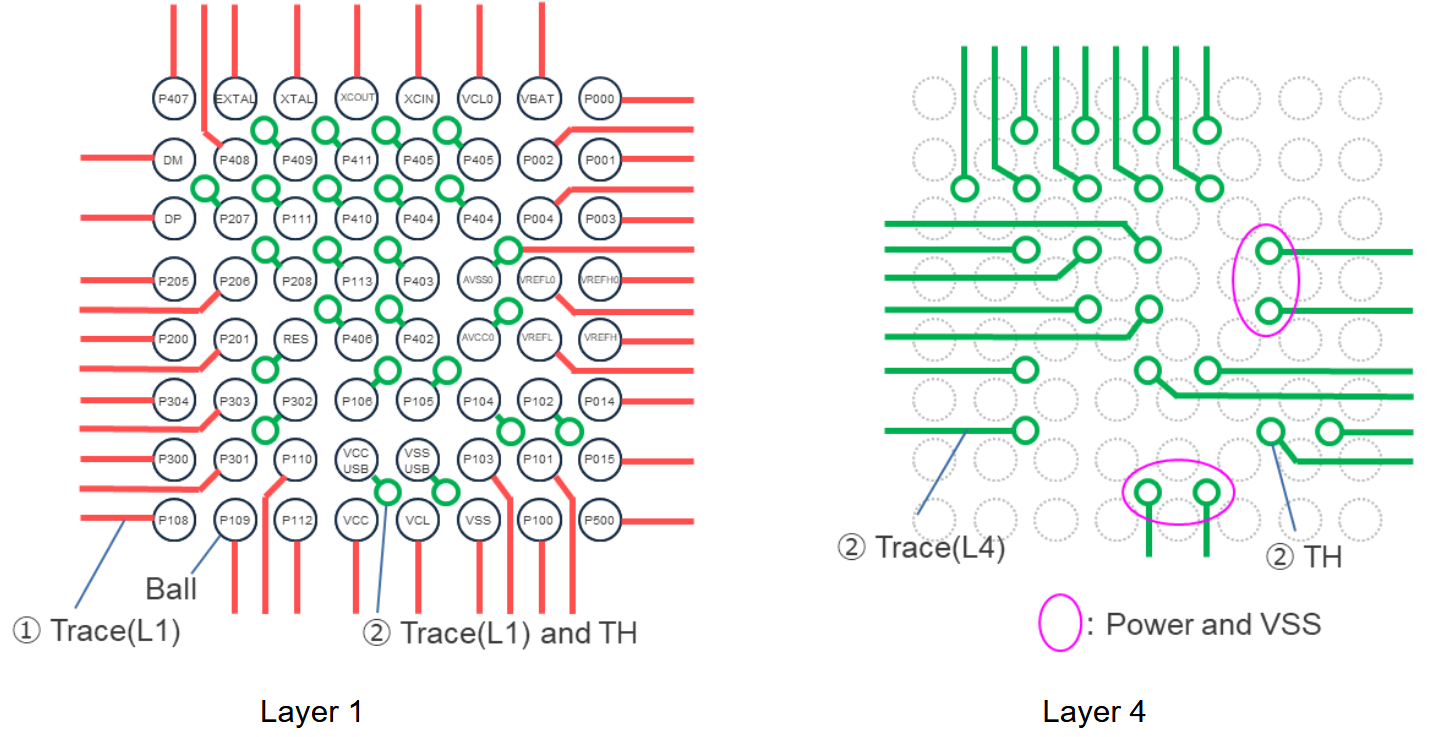
Figure 18, Example of layout for Layer 1 and Layer 4 of a 64 (8×8) BGA full grid (Top View)
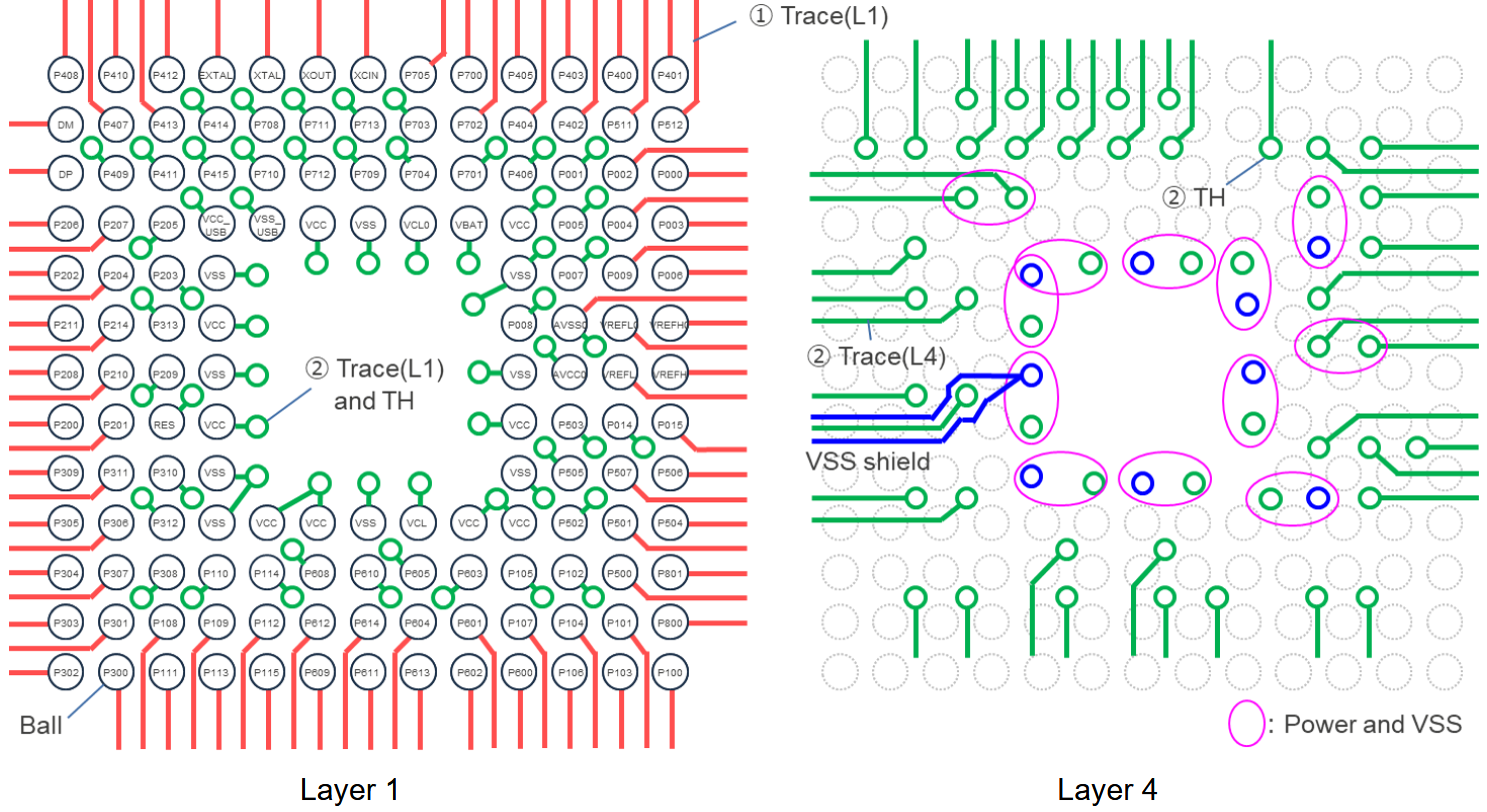
Figure 19, Example of layout for Layer 1 and 4 of a 144(13×13) BGA outer perimeter 4 rows (Top View)
Revision history

General Precautions in the Handling of Microprocessing Unit and Microcontroller Unit Products
The following usage notes are applicable to all Microprocessing unit and Microcontroller unit products from Renesas. For detailed usage notes on the products covered by this document, refer to the relevant sections of the document as well as any technical updates that have been issued for the products.
- Precaution against Electrostatic Discharge (ESD)
A strong electrical field, when exposed to a CMOS device, can cause destruction of the gate oxide and ultimately degrade the device operation. Steps must be taken to stop the generation of static electricity as much as possible, and quickly dissipate it when it occurs. Environmental control must be adequate. When it is dry, a humidifier should be used. This is recommended to avoid using insulators that can easily build up static electricity. Semiconductor devices must be stored and transported in an anti-static container, static shielding bag or conductive material. All test and measurement tools including work benches and floors must be grounded. The operator must also be grounded using a wrist strap. Semiconductor devices must not be touched with bare hands. Similar precautions must be taken for printed circuit boards with mounted semiconductor devices. - Processing at power-on
The state of the product is undefined at the time when power is supplied. The states of internal circuits in the LSI are indeterminate and the states of register settings and pins are undefined at the time when power is supplied. In a finished product where the reset signal is applied to the external reset pin, the states of pins are not guaranteed from the time when power is supplied until the reset process is completed. In a similar way, the states of pins in a product that is reset by an on-chip power-on reset function are not guaranteed from the time when power is supplied until the power reaches the level at which resetting is specified. - Input of signal during power-off state
Do not input signals or an I/O pull-up power supply while the device is powered off. The current injection that results from input of such a signal or I/O pull-up power supply may cause malfunction and the abnormal current that passes in the device at this time may cause degradation of internal elements. Follow the guideline for input signal during power-off state as described in your product documentation. - Handling of unused pins
Handle unused pins in accordance with the directions given under handling of unused pins in the manual. The input pins of CMOS products are generally in the high-impedance state. In operation with an unused pin in the open-circuit state, extra electromagnetic noise is induced in the vicinity of the LSI, an associated shoot-through current flows internally, and malfunctions occur due to the false recognition of the pin state as an input signal become possible. - Clock signals
After applying a reset, only release the reset line after the operating clock signal becomes stable. When switching the clock signal during program execution, wait until the target clock signal is stabilized. When the clock signal is generated with an external resonator or from an external oscillator during a reset, ensure that the reset line is only released after full stabilization of the clock signal. Additionally, when switching to a clock signal produced with an external resonator or by an external oscillator while program execution is in progress, wait until the target clock signal is stable. - Voltage application waveform at input pin
Waveform distortion due to input noise or a reflected wave may cause malfunction. If the input of the CMOS device stays in the area between Vɪɩ (Max.) and Vɪʜ (Min.) due to noise, for example, the device may malfunction. Take care to prevent chattering noise from entering the device when the input level is fixed, and also in the transition period when the input level passes through the area between Vɪɩ (Max.) and Vɪʜ (Min.).
Notice
- Descriptions of circuits, software and other related information in this document are provided only to illustrate the operation of semiconductor products and application examples. You are fully responsible for the incorporation or any other use of the circuits, software, and information in the design of your product or system. Renesas Electronics disclaims any and all liability for any losses and damages incurred by you or third parties arising from the use of these circuits, software, or information.
- Renesas Electronics hereby expressly disclaims any warranties against and liability for infringement or any other claims involving patents, copyrights, or other intellectual property rights of third parties, by or arising from the use of Renesas Electronics products or technical information described in this document, including but not limited to, the product data, drawings, charts, programs, algorithms, and application examples.
- No license, express, implied or otherwise, is granted hereby under any patents, copyrights or other intellectual property rights of Renesas Electronics or others.
- You shall be responsible for determining what licenses are required from any third parties, and obtaining such licenses for the lawful import, export, manufacture, sales, utilization, distribution or other disposal of any products incorporating Renesas Electronics products, if required.
- You shall not alter, modify, copy, or reverse engineer any Renesas Electronics product, whether in whole or in part. Renesas Electronics disclaims any and all liability for any losses or damages incurred by you or third parties arising from such alteration, modification, copying or reverse engineering.
- Renesas Electronics products are classified according to the following two quality grades: “Standard” and “High Quality”. The intended applications for each Renesas Electronics product depends on the product’s quality grade, as indicated below.
“Standard”: Computers; office equipment; communications equipment; test and measurement equipment; audio and visual equipment; home electronic appliances; machine tools; personal electronic equipment; industrial robots; etc.
“High Quality”: Transportation equipment (automobiles, trains, ships, etc.); traffic control (traffic lights); large-scale communication equipment; key financial terminal systems; safety control equipment; etc.
Unless expressly designated as a high reliability product or a product for harsh environments in a Renesas Electronics data sheet or other Renesas Electronics document, Renesas Electronics products are not intended or authorized for use in products or systems that may pose a direct threat to human life or bodily injury (artificial life support devices or systems; surgical implantations; etc.), or may cause serious property damage (space system; undersea repeaters; nuclear power control systems; aircraft control systems; key plant systems; military equipment; etc.). Renesas Electronics disclaims any and all liability for any damages or losses incurred by you or any third parties arising from the use of any Renesas Electronics product that is inconsistent with any Renesas Electronics data sheet, user’s manual or other Renesas Electronics document. - No semiconductor product is absolutely secure. Notwithstanding any security measures or features that may be implemented in Renesas Electronics hardware or software products, Renesas Electronics shall have absolutely no liability arising out of any vulnerability or security breach, including but not limited to any unauthorized access to or use of a Renesas Electronics product or a system that uses a Renesas Electronics product. RENESAS ELECTRONICS DOES NOT WARRANT OR GUARANTEE THAT RENESAS ELECTRONICS PRODUCTS, OR ANY SYSTEMS CREATED USING RENESAS ELECTRONICS PRODUCTS WILL BE INVULNERABLE OR FREE FROM CORRUPTION, ATTACK, VIRUSES, INTERFERENCE, HACKING, DATA LOSS OR THEFT, OR OTHER SECURITY INTRUSION (“Vulnerability Issues”). RENESAS ELECTRONICS DISCLAIMS ANY AND ALL RESPONSIBILITY OR LIABILITY ARISING FROM OR RELATED TO ANY VULNERABILITY ISSUES. FURTHERMORE, TO THE EXTENT PERMITTED BY APPLICABLE LAW, RENESAS ELECTRONICS DISCLAIMS ANY AND ALL WARRANTIES, EXPRESS OR IMPLIED, WITH RESPECT TO THIS DOCUMENT AND ANY RELATED OR ACCOMPANYING SOFTWARE OR HARDWARE, INCLUDING BUT NOT LIMITED TO THE IMPLIED WARRANTIES OF MERCHANTABILITY, OR FITNESS FOR A PARTICULAR PURPOSE.
- When using Renesas Electronics products, refer to the latest product information (data sheets, user’s manuals, application notes, “General Notes for Handling and Using Semiconductor Devices” in the reliability handbook, etc.), and ensure that usage conditions are within the ranges specified by Renesas Electronics with respect to maximum ratings, operating power supply voltage range, heat dissipation characteristics, installation, etc. Renesas Electronics disclaims any and all liability for any malfunctions, failure or accident arising out of the use of Renesas Electronics products outside of such specified ranges.
- Although Renesas Electronics endeavors to improve the quality and reliability of Renesas Electronics products, semiconductor products have specific characteristics, such as the occurrence of failure at a certain rate and malfunctions under certain use conditions. Unless designated as a high reliability product or a product for harsh environments in a Renesas Electronics data sheet or other Renesas Electronics document, Renesas Electronics products are not subject to radiation resistance design. You are responsible for implementing safety measures to guard against the possibility of bodily injury, injury or damage caused by fire, and/or danger to the public in the event of a failure or malfunction of Renesas Electronics products, such as safety design for hardware and software, including but not limited to redundancy, fire control and malfunction prevention, appropriate treatment for aging degradation or any other appropriate measures. Because the evaluation of microcomputer software alone is very difficult and impractical, you are responsible for evaluating the safety of the final products or systems manufactured by you.
- Please contact a Renesas Electronics sales office for details as to environmental matters such as the environmental compatibility of each Renesas Electronics product. You are responsible for carefully and sufficiently investigating applicable laws and regulations that regulate the inclusion or use of controlled substances, including without limitation, the EU RoHS Directive, and using Renesas Electronics products in compliance with all these applicable laws and regulations. Renesas Electronics disclaims any and all liability for damages or losses occurring as a result of your noncompliance with applicable laws and regulations.
- Renesas Electronics products and technologies shall not be used for or incorporated into any products or systems whose manufacture, use, or sale is prohibited under any applicable domestic or foreign laws or regulations. You shall comply with any applicable export control laws and regulations promulgated and administered by the governments of any countries asserting jurisdiction over the parties or transactions.
- It is the responsibility of the buyer or distributor of Renesas Electronics products, or any other party who distributes, disposes of, or otherwise sells or transfers the product to a third party, to notify such third party in advance of the contents and conditions set forth in this document.
- This document shall not be reprinted, reproduced or duplicated in any form, in whole or in part, without prior written consent of Renesas Electronics.
- Please contact a Renesas Electronics sales office if you have any questions regarding the information contained in this document or Renesas Electronics products.
(Note1) “Renesas Electronics” as used in this document means Renesas Electronics Corporation and also includes its directly or indirectly controlled subsidiaries.
(Note2) “Renesas Electronics product(s)” means any product developed or manufactured by or for Renesas Electronics.
Corporate Headquarters
TOYOSU FORESIA, 3-2-24 Toyosu,
Koto-ku, Tokyo 135-0061, Japan
www.renesas.com
Contact information
For further information on a product, technology, the most up-to-date version of a document, or your nearest sales office, please visit:
www.renesas.com/contact/
Trademarks
Renesas and the Renesas logo are trademarks of Renesas Electronics Corporation. All trademarks and registered trademarks are the property of their respective owners.
© 2021 Renesas Electronics Corporation. All rights reserved.
Documents / Resources
 |
RENESAS RA family, RX family 32-Bit Arm Cortex-M Microcontrollers [pdf] Owner's Manual R01AN7402EJ0100, RA family RX family 32-Bit Arm Cortex-M Microcontrollers, RA family RX family, 32-Bit Arm Cortex-M Microcontrollers, Arm Cortex-M Microcontrollers, Cortex-M Microcontrollers, Microcontrollers |