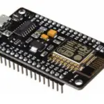
DEBIX Model A Single Board Computer User Guide

Version: V2.0 (2023-08)
Complied by: Polyhex Technology Company Limited (http://www.polyhex.net/)
DEBIX SOM A is the first System on Module in the DEBIX industrial computer family. Just likeDEBIX Model A single board computer, it is based on NXP i.MX 8M Plus processor withaNeural Processing Unit (NPU) operating at up to 2.3 TOPS, bringing us the samepowerful system performance.
Figure 1 DEBIX SOM A

| REVISION HISTORY | ||
| Rev. | Date | Description |
| 1.0 | 2022.12.01 | First edition |
| 1.1 | 2023.02.23 | Added Chapter 1.6 Accessories cable for DEBIX SOM A I/OBoard. |
| 1.2 | 2023.04.23 | Added eMMC formatting procedure and camera adapter boardcontents. |
| 2.0 | 2023.07.29 | Overall optimization of documentation, separate user manual foradd-on boards. |
Chapter 1 Security
Safety Precaution
This document inform how to make each cable connection. In most cases, you will simplyneed to connect a standard cable. Table 1 Terms and conventions
| Symbol | Meaning |
Warning! |
Always disconnect the power cord from the chassis whenever there is no workload required on it. Do not connect the power cable while the power is on. A sudden rush of power can damage sensitive electronic components. Only experienced electricians should open the chassis. |
Caution! |
Always ground yourself to remove any static electric charge before touching DEBIX product. Modern electronic devices are very sensitive to electric charges. Use a grounding wrist strap at all times. Place all electronic components on a static-dissipative surface or in a static-shielded bag. |
Safety Instruction
To avoid malfunction or damage to this product please observe the following:
- Disconnect the device from the DC power supply before cleaning. Use a damp cloth. Donot use liquid detergents or spray-on detergents.
- Keep the device away from moisture.
- During installation, set the device down on a reliable surface. Drops and bumps will leadtodamage.
- Before connecting the power supply, ensure that the voltage is in the required range, andthe way of wiring is correct.
- Carefully put the power cable in place to avoid stepping on it.
- If the device is not used for a long time, power it off to avoid damage caused by sudden
- Do not pour liquid into the venting holes of the enclosure, as this could cause fire or electric shock.
- For safety reasons, the device can only be disassembled by professional personnel.
- If one of the following situations occur, get the equipment checked by service personnel The power cord or plug is damaged. Liquid has penetrated into the equipment.
- The equipment has been exposed to moisture.
- The equipment does not work well, or you cannot get it to work according to the user’s manual.
- The equipment has been dropped and damaged.
- The equipment has obvious signs of breakage.
- Do not place the device outside the specified ambient temperature range. This will damage the machine. It needs to be kept in an environment at controlled temperature.
- Due to the sensitive nature of the equipment, it must be stored in a restricted access location, only accessible by qualified engineer
DISCLAIMER: Polyhex disclaims all responsibility for the accuracy of any statement of thisinstructional document
Declaration of Compliance
This product has passed the following certifications:
Table 2 Compliance Certification
| Symbol | Meaning |
 |
This equipment has passed CE certified. |
 |
This equipment is manufactured in compliance with RoHS regulations. |
 |
This equipment has passed UKCA certified. |
 |
This equipment has passed FCC certified. |
 |
This equipment has passed PSE certified. |
 |
This equipment has passed C-Tick certified. |
 |
This equipment is manufactured in compliance with RCM regulations. |
Technical Support
- Visit DEBIX website https://www.debix.io/ where you can find the latest information about the product.
- Contact your distributor, sales representative or Polyhex’s customer service center for technical support if you need additional assistance. Please have the following infoready before you call:
- Product name and memory size
- Description of your peripheral attachments
- Description of your software(operating system, version, application software, etc.)
- A complete description of the problem
- The exact wording of any error messages
Discord Community (recommended): https://discord.com/invite/adaHHaDkH2
Email: info@polyhex.net
Chapter 2 DEBIX SOMAIntroduction
DEBIX SOM A is an embedded SOM (system on module) board based on NXP i.MX8MPlus, with commercial-grade and industrial-grade CPU options, it can be widely used inmachinevision and machine learning, advanced multimedia, smart city, edge Computing andother scenarios that require high reliability
- Main features:
- Powerful quad-core Arm® Cortex®-A53 CPU with a neural processing unit (NPU) withacomputing speed up to 2.3TOPS
- Two vision signal processors (ISP) and two camera inputs for efficient vision system
- In terms of multimedia, video codec (including H.265, H.264), 3D/2D image accelerationand various audio and voice functions
- Real-time control of Cortex-M7.
- Powerful network control provided by CAN FD, supporting dual Gigabit Ethernet, oneof which supports TSN
- High industrial reliability with DRAM inline ECC
- Specially designed for harsh environmental conditions and temperature changes, thewide temperature range of the CPU from -40°C to 105°C makes it suitable for extremeindustrial environments, transportation, industrial control and other fields.
- Support for Ubuntu, Android, Yocto, Windows 10 IoT
Overview
Figure 2 DEBIX SOM A Front

Figure 3 DEBIX SOM A Back

DEBIX SOM A utilizes NXP i.MX 8M Plus as Soc, supports dual Gigabit Ethernet, dual imagesignal processor and dual camera input, the data specifications are as follows:
Table 3 DEBIX SOM A specification
| System | |
| CPU | i.MX 8M Plus, 4 x Cortex-A53 up to 1.8GHz, with 2.3TOPS computingpower NPU, and C520L 3D GPU and GC7000UltraLite 3D GPU |
| Memory | 2GB LPDDR4 (1GB/4GB/8BG optional) |
| Storage |
|
| OS | Ubuntu,Android11,Yocto-L5.10.72_2.2.0,Windows 10 IoT EnterpriseNOTE Only 8GB LPDDR4 supports Windows 10 IoT Enterprise. |
| Communication | |
| Gigabit Network | 2 x Gigabit Ethernet controller, one of which supports Time SensitiveNetworking (TSN) |
| Video & Audio | |
| HDMI | 1 x HDMI 2.0a, supports 3840 x 2160 @30Hz, 1920 x 1080 @120Hz,1920 x 1080 @60Hz |
| LVDS | 1 x LVDS, supports 4Lane and 8Lane |
| MIPI DSI | 1 x MIPI DSI, supports 2560 x 1080 @60Hz |
| MIPI CSI | 2 x MIPI CSI |
| Audio | Up to 6 x SAI (Simultaneous Audio Interface), HiFi4 DSP, 1 x SPDIFIN, 1 x SPDIF OUTNOTE1 x SAI 8 TX and 8 RX channels, 1 x SAI 4 TX and 4 RX channels, 2 x SAI 2 TX and 2 RX channels, 2x SAI 1 TX and 1RX channels, each SAI supports I2S and AC97 |
| External I/O Interface | |
| USB | 2 x USB 3.0 |
| UART | Up to 4 x UART |
| I2C | Up to 6 x I2C, leading to five I2C, i.e. I2C2~I2C6 (2 of them aremultiplexed as SD1), I2C1 can’t be configured. |
| SDIO | 2 x SDIO 3.0 |
| SPI | Up to 3 x ECSPI |
| PCIe | 1 x PCIe Gen3 |
| CAN | 2 x CAN |
| GPIO | Default 13 x GPIO, other function pins can be configured as GPIOthrough software |
| Power Supply | |
| Power Input | 3.5V~5V |
| Mechanical & Environmental | |
| Connector | 4 x double-sided contact board-to-board Plug connectors (model BB51024A-R80-10-32), 2 x 40pin/0.5mm pitch, matching varioussocket heights |
| Size (L x W x H) | 60.0mm x 40.0mm x 5.6mm |
| Weight | 23g |
| OperatingTemperature | 1) Industrial grade: -20°C~70°C2) Industrial grade: -40°C~85°C |
Composition
DEBIX SOM A consists of different computer components. The most important component isthe “brain” of the computer, the system-on-chip (SoC) in the center of the motherboard. The SoC contains most of the components of the computer, often containing both thecentra processing unit (CPU) and the graphics processing unit (GPU). DEBIX SOMAhas RandomMemory (RAM), eMMC, and PMIC (PCA9450C), which is used to manage the power devicesof the host machine, as shown in the figure figure:
Figure 4 DEBIX SOM A

Interface
DEBIX SOM A has 4 external board-to-board Plug connectors, the model isBB51024A-R80-10-32, 2x 40pin/0.5mm pitch, matching 4 socket connectors of different heights, the model is BB51024W-R80- 30-32, BB51024W-R80-35-32, BB51024W-R80-40-32, BB51024W-R80-45-32, used to connect DEBIX SOM A I/O Board.
Figure 5

The table below lists the pinouts of the four connectors of DEBIX SOMA, and lists thepinnames of the CPU corresponding to each pin.
Table 4 Header description of
| Table Column Name | Meaning |
| Default | The function pin definition we are using now (the definition given in the schematic diagram) |
| BALL_NAME | The pin name of the corresponding CPU |
| BALL | CPU pin number |
J3 Pinout
Table 5 J3 Pinout
| Pin | Default | BALL_NAME | BALL | NOTE |
| Pin1 | GND | |||
| Pin2 | GND |
| Pin3 | GPIO1_IO06 | GPIO1_IO06 | A3 | NVCC_GPIO, 1V8, Input with PD |
| Pin4 | GPIO1_IO15 | GPIO1_IO15 | B5 | NVCC_GPIO, 1V8, Input with PD |
| Pin5 | GPIO1_IO05 | GPIO1_IO05 | B4 | NVCC_GPIO, 1V8, Output high during reset, input with PU after reset |
| Pin6 | GPIO1_IO14 | GPIO1_IO14 | A4 | NVCC_GPIO, 1V8, Input with PD |
| Pin7 | GPIO1_IO01 | GPIO1_IO01 | E8 | NVCC_GPIO, 1V8, Output low during reset, input with PD after reset |
| Pin8 | GPIO1_IO13 | GPIO1_IO13 | A6 | NVCC_GPIO, 1V8, Input with PD |
| Pin9 | GPIO1_IO00 | GPIO1_IO00 | A7 | NVCC_GPIO, 1V8, Input with PD |
| Pin10 | GPIO1_IO12 | GPIO1_IO12 | A5 | NVCC_GPIO, 1V8, Input with PD |
| Pin11 | GND | |||
| Pin12 | GPIO1_IO11 | GPIO1_IO11 | D8 | NVCC_GPIO, 1V8, Input with PD |
| Pin13 | USB1_RXN | USB1_RX_N | B9 | VDD_USB_3P3, 3V3, Input |
| Pin14 | GPIO1_IO10 | GPIO1_IO10 | B7 | NVCC_GPIO, 1V8, Input with PD |
| Pin15 | USB1_RXP | USB1_RX_P | A9 | VDD_USB_3P3, 3V3, Input |
| Pin16 | GPIO1_IO09 | GPIO1_IO09 | B8 | NVCC_GPIO, 1V8, Input with PD |
| Pin17 | GND | |||
| Pin18 | GPIO1_IO08 | GPIO1_IO08 | A8 | NVCC_GPIO, 1V8, Input with PD |
| Pin19 | USB1_TXN | USB1_TX_N | B10 | VDD_USB_3P3, 3V3, Output |
| Pin20 | GPIO1_IO07 | GPIO1_IO07 | F6 | NVCC_GPIO, 1V8, Input with PD |
| Pin21 | USB1_TXP | USB1_TX_P | A10 | VDD_USB_3P3, 3V3, Output |
| Pin22 | GND | |||
| Pin23 | GND | |||
| Pin24 | USB1_DN | USB1_D_N | E10 | VDD_USB_3P3, 3V3, Input |
| Pin25 | USB2_RXN | USB2_RX_N | B12 | VDD_USB_3P3, 3V3, Input |
| Pin26 | USB1_DP | USB1_D_P | D10 | VDD_USB_3P3, 3V3, Input |
| Pin27 | USB2_RXP | USB2_RX_P | A12 | VDD_USB_3P3, 3V3, Input |
| Pin28 | GND | |||
| Pin29 | GND | |||
| Pin30 | USB2_DN | USB2_D_N | E14 | VDD_USB_3P3, 3V3, Input |
| Pin31 | USB2_TXN | USB2_TX_N | B13 | VDD_USB_3P3, 3V3, Output |
| Pin32 | USB2_DP | USB2_D_P | D14 | VDD_USB_3P3, 3V3, Input |
| Pin33 | USB2_TXP | USB2_TX_P | A13 | VDD_USB_3P3, 3V3, Output |
| Pin34 | GND | |||
| Pin35 | GND | |||
| Pin36 | USB1_VBUS_3V 3 | USB1_VBUS | A11 | VDD_USB_3P3, 3.3V, Input |
| Pin37 | PCIE_CLKN | PCIE_REF_PAD_CLK_ N | E16 | VDD_PCI_1P8, 1V8, High-Z |
| Pin38 | USB2_VBUS_3V 3 | USB2_VBUS | D12 | VDD_USB_3P3, 3.3V, Input |
| Pin39 | PCIE_CLKP | PCIE_REF_PAD_CLK_ P | D16 | VDD_PCI_1P8, 1V8, High-Z |
| Pin40 | JTAG_TMS | JTAG_TMS | G14 | NVCC_JTAG, 1V8, Input with PU |
| Pin41 | GND | |||
| Pin42 | JTAG_TDO | JTAG_TDO | F14 | NVCC_JTAG, 1V8, Input with PU |
| Pin43 | PCIE_RXN | PCIE_RXN_N | B14 | VDD_PCI_1P8, 1V8, Input, High-Z |
| Pin44 | JTAG_TDI | JTAG_TDI | G16 | NVCC_JTAG, 1V8, Input with PU |
| Pin45 | PCIE_RXP | PCIE_RXN_P | A14 | VDD_PCI_1P8, 1V8, Input, High-Z |
| Pin46 | JTAG_MOD | JTAG_MOD | G20 | NVCC_JTAG, 1V8, Input with PD |
| Pin47 | GND | |||
| Pin48 | JTAG_TCK | JTAG_TCK | G18 | NVCC_JTAG, 1V8, Input with PU |
| Pin49 | PCIE_TXN | PCIE_TXN_N | B15 | VDD_PCI_1P8, 1V8, Output, High-Z |
| Pin50 | GND |
| Pin51 | PCIE_TXP | PCIE_TXN_P | A15 | VDD_PCI_1P8, 1V8, Output, High-Z |
| Pin52 | CSI1_DN0 | MIPI_CSI1_D0_N | E18 | VDD_MIPI_1P8, 1V8, Input |
| Pin53 | GND | |||
| Pin54 | CSI1_DP0 | MIPI_CSI1_D0_P | D18 | VDD_MIPI_1P8, 1V8, Input |
| Pin55 | DSI_DN0 | MIPI_DSI1_D0_N | B16 | VDD_MIPI_1P8, 1V8, Output low |
| Pin56 | GND | |||
| Pin57 | DSI_DP0 | MIPI_DSI1_D0_P | A16 | VDD_MIPI_1P8, 1V8, Output low |
| Pin58 | CSI1_DN1 | MIPI_CSI1_D1_N | E20 | VDD_MIPI_1P8, 1V8, Input |
| Pin59 | DSI_DN1 | MIPI_DSI1_D1_N | B17 | VDD_MIPI_1P8, 1V8, Output low |
| Pin60 | CSI1_DP1 | MIPI_CSI1_D1_P | D20 | VDD_MIPI_1P8, 1V8, Input |
| Pin61 | DSI_DP1 | MIPI_DSI1_D1_P | A17 | VDD_MIPI_1P8, 1V8, Output low |
| Pin62 | GND | |||
| Pin63 | GND | |||
| Pin64 | CSI1_CKN | MIPI_CSI1_CLK_N | E22 | VDD_MIPI_1P8, 1V8, Input |
| Pin65 | DSI_CKN | MIPI_DSI1_CLK_N | B18 | VDD_MIPI_1P8, 1V8, Output low |
| Pin66 | CSI1_CKP | MIPI_CSI1_CLK_P | D22 | VDD_MIPI_1P8, 1V8, Input |
| Pin67 | DSI_CKP | MIPI_DSI1_CLK_P | A18 | VDD_MIPI_1P8, 1V8, Output low |
| Pin68 | GND | |||
| Pin69 | GND | |||
| Pin70 | CSI1_DN2 | MIPI_CSI1_D2_N | E24 | VDD_MIPI_1P8, 1V8, Input |
| Pin71 | DSI_DN2 | MIPI_DSI1_D2_N | B19 | VDD_MIPI_1P8, 1V8, Output low |
| Pin72 | CSI1_DP2 | MIPI_CSI1_D2_P | D24 | VDD_MIPI_1P8, 1V8, Input |
| Pin73 | DSI_DP2 | MIPI_DSI1_D2_P | A19 | VDD_MIPI_1P8, 1V8, Output low |
| Pin74 | GND | |||
| Pin75 | DSI_DN3 | MIPI_DSI1_D3_N | B20 | VDD_MIPI_1P8, 1V8, Output low |
| Pin76 | CSI1_DN3 | MIPI_CSI1_D3_N | E26 | VDD_MIPI_1P8, 1V8, Input |
| Pin77 | DSI_DP3 | MIPI_DSI1_D3_P | A20 | VDD_MIPI_1P8, 1V8, Output low |
| Pin78 | CSI1_DP3 | MIPI_CSI1_D3_P | D26 | VDD_MIPI_1P8, 1V8, Input |
| Pin79 | GND | |||
| Pin80 | GND |
J4 Pinout
Table 6 J4 Pinout
| Pin | Default | BALL_NAME | BALL | NOTE |
| Pin1 | GND | |||
| Pin2 | GND | |||
| Pin3 | LVDS1_TX0_P | LVDS1_D0_P | A26 | VDD_LVDS_1P8, 1V8 |
| Pin4 | CSI2_DN3 | MIPI_CSI2_D3_N | B21 | VDD_MIPI_1P8, 1V8, Input |
| Pin5 | LVDS1_TX0_N | LVDS1_D0_N | B26 | VDD_LVDS_1P8, 1V8 |
| Pin6 | CSI2_DP3 | MIPI_CSI2_D3_P | A21 | VDD_MIPI_1P8, 1V8, Input |
| Pin7 | GND | |||
| Pin8 | GND | |||
| Pin9 | LVDS1_TX1_P | LVDS1_D1_P | A27 | VDD_LVDS_1P8, 1V8 |
| Pin10 | CSI2_DN2 | MIPI_DSI2_D2_N | B22 | VDD_MIPI_1P8, 1V8, Input |
| Pin11 | LVDS1_TX1_N | LVDS1_D1_N | B27 | VDD_LVDS_1P8, 1V8 |
| Pin12 | CSI2_DP2 | MIPI_DSI2_D2_P | A22 | VDD_MIPI_1P8, 1V8, Input |
| Pin13 | GND | |||
| Pin14 | GND | |||
| Pin15 | LVDS1_CLK_P | LVDS1_CLK_P | A28 | VDD_LVDS_1P8, 1V8 |
| Pin16 | CSI2_CKN | MIPI_CSI2_CLK_N | B23 | VDD_MIPI_1P8, 1V8, Input |
| Pin17 | LVDS1_CLK_N | LVDS1_CLK_N | B28 | VDD_LVDS_1P8, 1V8 |
| Pin18 | CSI2_CKP | MIPI_CSI2_CLK_P | A23 | VDD_MIPI_1P8, 1V8, Input |
| Pin19 | GND |
| Pin20 | GND | |||
| Pin21 | LVDS1_TX2_P | LVDS1_D2_P | B29 | VDD_LVDS_1P8, 1V8 |
| Pin22 | CSI2_DN1 | MIPI_CSI2_D1_N | B24 | VDD_MIPI_1P8, 1V8, Input |
| Pin23 | LVDS1_TX2_N | LVDS1_D2_N | C28 | VDD_LVDS_1P8, 1V8 |
| Pin24 | CSI2_DP1 | MIPI_CSI2_D1_P | A24 | VDD_MIPI_1P8, 1V8, Input |
| Pin25 | GND | |||
| Pin26 | GND | |||
| Pin27 | LVDS1_TX3_P | LVDS1_D3_P | C29 | VDD_LVDS_1P8, 1V8 |
| Pin28 | CSI2_DN0 | MIPI_CSI2_D0_N | B25 | VDD_MIPI_1P8, 1V8, Input |
| Pin29 | LVDS1_TX3_N | LVDS1_D3_N | D28 | VDD_LVDS_1P8, 1V8 |
| Pin30 | CSI2_DP0 | MIPI_CSI2_D0_P | A25 | VDD_MIPI_1P8, 1V8, Input |
| Pin31 | GND | |||
| Pin32 | GND | |||
| Pin33 | LVDS0_TX0_P | LVDS0_D0_P | D29 | VDD_LVDS_1P8, 1V8 |
| Pin34 | NAND_DQS | NAND_DQS | R26 | NVCC_NAND, 1V8, Input with PD |
| Pin35 | LVDS0_TX0_N | LVDS0_D0_N | E28 | VDD_LVDS_1P8, 1V8 |
| Pin36 | ONOFF | ONOFF | G22 | NVCC_SNVS, 1V8, Input with PU |
| Pin37 | GND | |||
| Pin38 | POR_B | POR_B | J29 | NVCC_SNVS, 1V8, Input with PU |
| Pin39 | LVDS0_TX1_P | LVDS0_D1_P | E29 | VDD_LVDS_1P8, 1V8 |
| Pin40 | PMIC_ON_REQ | LVDS0_D1_P | F22 | NVCC_SNVS, 1V8, Output high with PU |
| Pin41 | LVDS0_TX1_N | LVDS0_D1_N | F28 | VDD_LVDS_1P8, 1V8 |
| Pin42 | GND | |||
| Pin43 | GND | |||
| Pin44 | BOOT_MODE0 | BOOT_MODE0 | G10 | NVCC_JTAG, 1V8, Input with PD |
| Pin45 | LVDS0_CLK_P | LVDS0_CLK_P | F29 | VDD_LVDS_1P8, 1V8 |
| Pin46 | BOOT_MODE1 | BOOT_MODE1 | F8 | NVCC_JTAG, 1V8, Input with PD |
| Pin47 | LVDS0_CLK_N | LVDS0_CLK_N | G28 | VDD_LVDS_1P8, 1V8 |
| Pin48 | BOOT_MODE2 | BOOT_MODE2 | G8 | NVCC_JTAG, 1V8, Input with PD |
| Pin49 | GND | |||
| Pin50 | BOOT_MODE3 | BOOT_MODE3 | G12 | NVCC_JTAG, 1V8, Input with PD |
| Pin51 | LVDS0_TX2_P | LVDS0_D2_P | G29 | VDD_LVDS_1P8, 1V8 |
| Pin52 | WDOG_B | GPIO1_IO02 | B6 | NVCC_GPIO, 1V8, Input with PU |
| Pin53 | LVDS0_TX2_N | LVDS0_D2_N | H28 | VDD_LVDS_1P8, 1V8 |
| Pin54 | GND | |||
| Pin55 | GND | |||
| Pin56 | CLKIN1 | CLKIN1 | K28 | NVCC_CLK, 1V8, Input with PD |
| Pin57 | LVDS0_TX3_P | LVDS0_D3_P | H29 | VDD_LVDS_1P8, 1V8 |
| Pin58 | GND | |||
| Pin59 | LVDS0_TX3_N | LVDS0_D3_N | J28 | VDD_LVDS_1P8, 1V8 |
| Pin60 | CLKOUT1 | CLKOUT1 | K29 | NVCC_CLK, 1V8, Output low |
| Pin61 | GND | |||
| Pin62 | GND | |||
| Pin63 | SD1_STROBE | SD1_STROBE | W26 | NVCC_SD1, 1V8, Input with PD |
| Pin64 | CLKIN2 | CLKIN2 | L28 | NVCC_CLK, 1V8, Input with PD |
| Pin65 | SD1_RESET_B | SD1_RESET_B | W25 | NVCC_SD1, 1V8, Input with PD |
| Pin66 | GND | |||
| Pin67 | SD1_CLK | SD1_CLK | W28 | NVCC_SD1, 1V8, Input with PD |
| Pin68 | CLKOUT2 | CLKOUT2 | L29 | NVCC_CLK, 1V8, Output low |
| Pin69 | SD1_CMD | SD1_CMD | W29 | NVCC_SD1, 1V8, Input with PD |
| Pin70 | GND | |||
| Pin71 | SD1_DATA0 | SD1_DATA0 | Y29 | NVCC_SD1, 1V8, Input with PD |
| Pin72 | SD1_DATA4 | SD1_DATA4 | U26 | NVCC_SD1, 1V8, Input with PD |
| Pin73 | SD1_DATA1 | SD1_DATA1 | Y28 | NVCC_SD1, 1V8, Input with PD |
| Pin74 | SD1_DATA5 | SD1_DATA5 | AA29 | NVCC_SD1, 1V8, Input with PD |
| Pin75 | SD1_DATA2 | SD1_DATA2 | V29 | NVCC_SD1, 1V8, Input with PD |
| Pin76 | SD1_DATA6 | SD1_DATA6 | AA28 | NVCC_SD1, 1V8, Input with PD |
| Pin77 | SD1_DATA3 | SD1_DATA3 | V28 | NVCC_SD1, 1V8, Input with PD |
| Pin78 | SD1_DATA7 | SD1_DATA7 | U25 | NVCC_SD1, 1V8, Input with PD |
| Pin79 | GND | |||
| Pin80 | GND |
J5 Pinout
Table 7 J5 Pinout
| Pin | Default | BALL_NAME | BALL | NOTE |
| Pin1 | GND | |||
| Pin2 | GND | |||
| Pin3 | I2C2_SCL | I2C2_SCL | AH6 | NVCC_I2C_UART, 1V8, Input with PD |
| Pin4 | UART1_TXD | UART1_TXD | AJ3 | NVCC_I2C_UART, 1V8, Input with PD |
| Pin5 | I2C2_SDA | I2C2_SDA | AE8 | NVCC_I2C_UART, 1V8, Input with PD |
| Pin6 | UART1_RXD | UART1_RXD | AD6 | NVCC_I2C_UART, 1V8, Input with PD |
| Pin7 | I2C3_SCL | I2C3_SCL | AJ7 | NVCC_I2C_UART, 1V8, Input with PD |
| Pin8 | UART1_CTS | UART3_RXD | AE6 | NVCC_I2C_UART, 1V8, Input with PD |
| Pin9 | I2C3_SDA | I2C3_SDA | AJ6 | NVCC_I2C_UART, 1V8, Input with PD |
| Pin10 | UART1_RTS | UART3_TXD | AJ4 | NVCC_I2C_UART, 1V8, Input with PD |
| Pin11 | I2C4_SCL | I2C4_SCL | AF8 | NVCC_I2C_UART, 1V8, Input with PD |
| Pin12 | UART2_TXD | UART2_TXD | AH4 | NVCC_I2C_UART, 1V8, Input with PD |
| Pin13 | I2C4_SDA | I2C4_SDA | AD8 | NVCC_I2C_UART, 1V8, Input with PD |
| Pin14 | UART2_RXD | UART2_RXD | AF6 | NVCC_I2C_UART, 1V8, Input with PD |
| Pin15 | GND |
| Pin16 | UART4_TXD | UART4_TXD | AH5 | NVCC_I2C_UART, 1V8, Input with PD |
| Pin17 | SAI1_TXC | SAI1_TXC | AJ12 | NVCC_SAI1_SAI5, 1V8, Input with PD |
| Pin18 | UART4_RXD | UART4_RXD | AJ5 | NVCC_I2C_UART, 1V8, Input with PD |
| Pin19 | SAI1_TXD0 | SAI1_TXD0 | AJ11 | NVCC_SAI1_SAI5, 1V8, Input with PD |
| Pin20 | GND | |||
| Pin21 | SAI1_TXD1 | SAI1_TXD1 | AJ10 | NVCC_SAI1_SAI5, 1V8, Input with PD |
| Pin22 | SAI1_RXFS | SAI1_RXFS | AJ9 | NVCC_SAI1_SAI5, 1V8, Input with PD |
| Pin23 | SAI1_TXD2 | SAI1_TXD2 | AH11 | NVCC_SAI1_SAI5, 1V8, Input with PD |
| Pin24 | SAI1_RXC | SAI1_RXC | AH8 | NVCC_SAI1_SAI5, 1V8, Input with PD |
| Pin25 | SAI1_TXD3 | SAI1_TXD3 | AD12 | NVCC_SAI1_SAI5, 1V8, Input with PD |
| Pin26 | SAI1_RXD0 | SAI1_RXD0 | AC10 | NVCC_SAI1_SAI5, 1V8, Input with PD |
| Pin27 | SAI1_TXD4 | SAI1_TXD4 | AH13 | NVCC_SAI1_SAI5, 1V8, Input with PD |
| Pin28 | SAI1_RXD1 | SAI1_RXD1 | AF10 | NVCC_SAI1_SAI5, 1V8, Input with PD |
| Pin29 | SAI1_TXD5 | SAI1_TXD5 | AH14 | NVCC_SAI1_SAI5, 1V8, Input with PD |
| Pin30 | SAI1_RXD2 | SAI1_RXD2 | AH9 | NVCC_SAI1_SAI5, 1V8, Input with PD |
| Pin31 | SAI1_TXD6 | SAI1_TXD6 | AC12 | NVCC_SAI1_SAI5, 1V8, Input with PD |
| Pin32 | SAI1_RXD3 | SAI1_RXD3 | AJ8 | NVCC_SAI1_SAI5, 1V8, Input with PD |
| Pin33 | SAI1_TXD7 | SAI1_TXD7 | AJ13 | NVCC_SAI1_SAI5, 1V8, Input with PD |
| Pin34 | SAI1_RXD4 | SAI1_RXD4 | AD10 | NVCC_SAI1_SAI5, 1V8, Input with PD |
| Pin35 | SAI1_TXFS | SAI1_TXFS | AF12 | NVCC_SAI1_SAI5, 1V8, Input with PD |
| Pin36 | SAI1_RXD5 | SAI1_RXD5 | AE10 | NVCC_SAI1_SAI5, 1V8, Input with PD |
| Pin37 | GND | |||
| Pin38 | SAI1_RXD6 | SAI1_RXD6 | AH10 | NVCC_SAI1_SAI5, 1V8, Input with PD |
| Pin39 | SAI5_RXD0 | SAI5_RXD0 | AE16 | NVCC_SAI1_SAI5, 1V8, Input with PD |
| Pin40 | SAI1_RXD7 | SAI1_RXD7 | AH12 | NVCC_SAI1_SAI5, 1V8, Input with PD |
| Pin41 | SAI5_RXD1 | SAI5_RXD1 | AD16 | NVCC_SAI1_SAI5, 1V8, Input with PD |
| Pin42 | SAI1_MCLK | SAI1_MCLK | AE12 | NVCC_SAI1_SAI5, 1V8, Input with PD |
| Pin43 | SAI5_RXD2 | SAI5_RXD2 | AF16 | NVCC_SAI1_SAI5, 1V8, Input with PD |
| Pin44 | GND | |||
| Pin45 | SAI5_RXD3 | SAI5_RXD3 | AE14 | NVCC_SAI1_SAI5, 1V8, Input with PD |
| Pin46 | SAI5_RXFS | SAI5_RXFS | AC14 | NVCC_SAI1_SAI5, 1V8, Input with PD |
| Pin47 | SAI2_TXC | SAI2_TXC | AH15 | NVCC_SAI2_SAI3_SPDIF, 1V8, Input with PD |
| Pin48 | SAI5_RXC | SAI5_RXC | AD14 | NVCC_SAI1_SAI5, 1V8, Input with PD |
| Pin49 | SAI2_TXFS | SAI2_TXFS | AJ17 | NVCC_SAI2_SAI3_SPDIF, 1V8, Input with PD |
| Pin50 | SAI5_MCLK | SAI5_MCLK | AF14 | NVCC_SAI1_SAI5, 1V8, Input with PD |
| Pin51 | SAI2_TXD | SAI2_TXD0 | AH16 | NVCC_SAI2_SAI3_SPDIF, 1V8, Input with PD |
| Pin52 | SAI2_RXFS | SAI2_RXFS | AH17 | NVCC_SAI1_SAI5, 1V8, Input with PD |
| Pin53 | SAI2_RXD | SAI2_RXD0 | AJ14 | NVCC_SAI2_SAI3_SPDIF, 1V8, Input with PD |
| Pin54 | SAI2_RXC | SAI2_RXC | AJ16 | NVCC_SAI1_SAI5, 1V8, Input with PD |
| Pin55 | SAI3_TXC | SAI3_TXC | AH19 | NVCC_SAI2_SAI3_SPDIF, 1V8, Input with PD |
| Pin56 | SAI2_MCLK | SAI2_MCLK | AJ15 | NVCC_SAI2_SAI3_SPDIF, 1V8, Input with PD |
| Pin57 | SAI3_TXFS | SAI3_TXFS | AC16 | NVCC_SAI2_SAI3_SPDIF, 1V8, Input with PD |
| Pin58 | SAI3_MCLK | SAI3_MCLK | AJ20 | NVCC_SAI2_SAI3_SPDIF, 1V8, Input with PD |
| Pin59 | SAI3_TXD | SAI3_TXD | AH18 | NVCC_SAI2_SAI3_SPDIF, 1V8, Input with PD |
| Pin60 | SAI3_RXC | SAI3_RXC | AJ18 | NVCC_SAI2_SAI3_SPDIF, 1V8, Input with PD |
| Pin61 | GND | |||
| Pin62 | SAI3_RXFS | SAI3_RXFS | AJ19 | NVCC_SAI2_SAI3_SPDIF, 1V8, Input with PD |
| Pin63 | ECSPI2_SCLK | ECSPI2_SCLK | AH21 | NVCC_ECSPI_HDMI, 1V8, Input with PD |
| Pin64 | SAI3_RXD | SAI3_RXD | AF18 | NVCC_SAI2_SAI3_SPDIF, 1V8, Input with PD |
| Pin65 | ECSPI2_SS0 | ECSPI2_SS0 | AJ22 | NVCC_ECSPI_HDMI, 1V8, Input with PD |
| Pin66 | SPDIF_TX | SPDIF_TX | AE18 | NVCC_SAI2_SAI3_SPDIF, 1V8, Input with PD |
| Pin67 | ECSPI2_MOSI | ECSPI2_MOSI | AJ21 | NVCC_ECSPI_HDMI, 1V8, Input with PD |
| Pin68 | SPDIF_RX | SPDIF_RX | AD18 | NVCC_SAI2_SAI3_SPDIF, 1V8, Input with PD |
| Pin69 | ECSPI2_MISO | ECSPI2_MISO | AH20 | NVCC_ECSPI_HDMI, 1V8, Input with PD |
| Pin70 | SPDIF_EXT_CL K | SPDIF_EXT_CLK | AC18 | NVCC_SAI2_SAI3_SPDIF, 1V8, Input with PD |
| Pin71 | HDMI_DDC_SCL | HDMI_DDC_SCL | AC22 | NVCC_ECSPI_HDMI, 1V8, Input with PD |
| Pin72 | UART3_CTS | ECSPI1_MISO | AD20 | NVCC_ECSPI_HDMI, 1V8, Input with PD |
| Pin73 | HDMI_DDC_SD A | HDMI_DDC_SDA | AF22 | NVCC_ECSPI_HDMI, 1V8, Input with PD |
| Pin74 | UART3_RTS | ECSPI1_SS0 | AE20 | NVCC_ECSPI_HDMI, 1V8, Input with PD |
| Pin75 | HDMI_HPD | HDMI_HPD | AE22 | NVCC_ECSPI_HDMI, 1V8, Input with PD |
| Pin76 | UART3_TXD | ECSPI1_MOSI | AC20 | NVCC_ECSPI_HDMI, 1V8, Input with PD |
| Pin77 | HDMI_CEC | HDMI_CEC | AD22 | NVCC_ECSPI_HDMI, 1V8, Input with PD |
| Pin78 | UART3_RXD | ECSPI1_SCLK | AF20 | NVCC_ECSPI_HDMI, 1V8, Input with PD |
| Pin79 | GND | |||
| Pin80 | GND |
J6 Pinout
Table 8 J6 Pinout
| Pin | Default | BALL_NAME | BALL | NOTE |
| Pin1 | GND | |||
| Pin2 | GND | |||
| Pin3 | EARC_N_HPD | EARC_N_HPD | AH22 | VDD_EARC_1P8, 1V8, Output |
| Pin4 | ENET_MDC | ENET_MDC | AH28 | NVCC_ENET, 1V8, Input with PD |
| Pin5 | EARC_P_UTIL | EARC_P_UTIL | AJ23 | VDD_EARC_1P8, 1V8, Output |
| Pin6 | ENET_MDIO | ENET_MDIO | AH29 | NVCC_ENET, 1V8, Input with PD |
| Pin7 | GND | |||
| Pin8 | ENET_TX_CTL | ENET_TX_CTL | AF24 | NVCC_ENET, 1V8, Input with PD |
| Pin9 | HDMI_TXCN | HDMI_TXC_N | AJ24 | VDD_HDMI_1P8, 1V8 |
| Pin10 | ENET_TXC | ENET_TXC | AE24 | NVCC_ENET, 1V8, Input with PD |
| Pin11 | HDMI_TXCP | HDMI_TXC_P | AH24 | VDD_HDMI_1P8, 1V8 |
| Pin12 | ENET_TD0 | ENET_TD0 | AC25 | NVCC_ENET, 1V8, Input with PD |
| Pin13 | GND | |||
| Pin14 | ENET_TD1 | ENET_TD1 | AE26 | NVCC_ENET, 1V8, Input with PD |
| Pin15 | HDMI_TXN0 | HDMI_TX0_N | AJ25 | VDD_HDMI_1P8, 1V8 |
| Pin16 | ENET_TD2 | ENET_TD2 | AF26 | NVCC_ENET, 1V8, Input with PD |
| Pin17 | HDMI_TXP0 | HDMI_TX0_P | AH25 | VDD_HDMI_1P8, 1V8 |
| Pin18 | ENET_TD3 | ENET_TD3 | AD24 | NVCC_ENET, 1V8, Input with PD |
| Pin19 | GND | |||
| Pin20 | ENET_RX_CTL | ENET_RX_CTL | AE28 | NVCC_ENET, 1V8, Input with PD |
| Pin21 | HDMI_TXN1 | HDMI_TX1_N | AJ26 | VDD_HDMI_1P8, 1V8 |
| Pin22 | ENET_RXC | ENET_RXC | AE29 | NVCC_ENET, 1V8, Input with PD |
| Pin23 | HDMI_TXP1 | HDMI_TX1_P | AH26 | VDD_HDMI_1P8, 1V8 |
| Pin24 | ENET_RD0 | ENET_RD0 | AG29 | NVCC_ENET, 1V8, Input with PD |
| Pin25 | GND | |||
| Pin26 | ENET_cRD1 | ENET_RD1 | AG28 | NVCC_ENET, 1V8, Input with PD |
| Pin27 | HDMI_TXN2 | HDMI_TX2_N | AJ27 | VDD_HDMI_1P8, 1V8 |
| Pin28 | ENET_RD2 | ENET_RD2 | AF29 | NVCC_ENET, 1V8, Input with PD |
| Pin29 | HDMI_TXP2 | HDMI_TX2_P | AH27 | VDD_HDMI_1P8, 1V8 |
| Pin30 | ENET_RD3 | ENET_RD3 | AF28 | NVCC_ENET, 1V8, Input with PD |
| Pin31 | GND | |||
| Pin32 | GND | |||
| Pin33 | SD2_DATA0 | SD2_DATA0 | AC28 | NVCC_SD2, 1V8, Input with PD |
| Pin34 | SD2_WP | SD2_WP | AC26 | NVCC_SD2, 1V8, Input with PD |
| Pin35 | SD2_DATA1 | SD2_DATA1 | AC29 | NVCC_SD2, 1V8, Input with PD |
| Pin36 | SD2_nCD | SD2_CD_B | AD29 | NVCC_SD2, 1V8, Input with PD |
| Pin37 | SD2_DATA2 | SD2_DATA2 | AA26 | NVCC_SD2, 1V8, Input with PD |
| Pin38 | SD2_CLK | SD2_CLK | AB29 | NVCC_SD2, 1V8, Input with PD |
| Pin39 | GND | |||
| Pin40 | SD2_CMD | SD2_CMD | AB28 | NVCC_SD2, 1V8, Input with PD |
| Pin41 | QSPIA_SCLK | NAND_ALE | N25 | NVCC_NAND, 1V8, Input with PD |
| Pin42 | SD2_DATA3 | SD2_DATA3 | AA25 | NVCC_SD2, 1V8, Input with PD |
| Pin43 | PMIC_32K_OUT | |||
| Pin44 | QSPIA_nSS0 | NAND_CE0_B | L26 | NVCC_NAND, 1V8, Input with PD |
| Pin45 | SYS_nRST | |||
| Pin46 | QSPIA_DATA0 | NAND_DATA00 | R25 | NVCC_NAND, 1V8, Input with PD |
| Pin47 | VSD_3V3 | |||
| Pin48 | QSPIA_DATA1 | NAND_DATA01 | L25 | NVCC_NAND, 1V8, Input with PD |
| Pin49 | VSD_3V3 | |||
| Pin50 | QSPIA_DATA2 | NAND_DATA02 | L24 | NVCC_NAND, 1V8, Input with PD |
| Pin51 | VSD_3V3 |
| Pin52 | QSPIA_DATA3 | NAND_DATA03 | N24 | NVCC_NAND, 1V8, Input with PD |
| Pin53 | VDD_3V3 | |||
| Pin54 | VDD_1V8 | |||
| Pin55 | VDD_3V3 | |||
| Pin56 | VDD_1V8 | |||
| Pin57 | VDD_3V3 | |||
| Pin58 | VDD_1V8 | |||
| Pin59 | VDD_3V3 | |||
| Pin60 | VDD_1V8 | |||
| Pin61 | GND | |||
| Pin62 | GND | |||
| Pin63 | GND | |||
| Pin64 | GND | |||
| Pin65 | GND | |||
| Pin66 | GND | |||
| Pin67 | GND | |||
| Pin68 | GND | |||
| Pin69 | GND | |||
| Pin70 | GND | |||
| Pin71 | VSYS_5V | |||
| Pin72 | VSYS_5V | |||
| Pin73 | VSYS_5V | |||
| Pin74 | VSYS_5V | |||
| Pin75 | VSYS_5V | |||
| Pin76 | VSYS_5V | |||
| Pin77 | VSYS_5V | |||
| Pin78 | VSYS_5V |
| Pin79 | VSYS_5V | |||
| Pin80 | VSYS_5V |
Packing List
- DEBIX SOM A Singer Board
Chapter 3 DEBIX SOMAI/OBoard
DEBIX SOM A I/O Board is a carrier board designed for DEBIX SOM A, which connectstoDEBIX SOM A through 4 double-sided board-to-board socket connectors on its front side. It’sall about full-featured interfaces supported by the core board based on i.MX 8MPlus, andprovides a perfect solution combining the functions required for industrial control, IoTconnection and multimedia.
For details of the interface and usage of DEBIX SOM A I/O board, please refer to DEBIXSOMA I/O BoardUser Manual.
Figure 6 DEBIX SOM A I/O Board

Chapter 4 Camera Adapter BoardforDEBIX
SOM A I/O Board
Camera Adapter Board is an add-on board designed for DEBIX SOM A I/OBoard to allow the connection with DEBIX Camera Modules. It has a FPC connector for the flexible flat cableof the camera module and a 2 x 10Pin connector for the CSI connection cable. For details of the interface and usage of Camera Adapter Board, please refer to Camera Adapter Board User Manual
Figure 7 Camera Adapter Board for DEBIX SOM A I/O Board

Documents / Resources
 |
DEBIX Model A Single Board Computer [pdf] User Guide Model A, Model A Single Board Computer, Single Board Computer, Board Computer, Computer |