FEASYCOM FSCBT9104DI Bluetooth Module

Copyright © 2013-2024 Shenzhen Feasycom Co., Ltd. All Rights Reserved.
Shenzhen Feasycom Co., Ltd reserves the right to make corrections, modifications, and other changes to its products, documentation, and services at any time. Customers are advised to obtain the latest relevant information before placing orders. In order to minimize product risks, customers should implement sufficient design and operational safeguards. Reproduction, transfer, distribution, or storage of any part or all of the contents in this document, in any form, without written permission from Shenzhen Feasycom Co., Ltd, is strictly prohibited
Revision History
| Version | Data | Notes | Author |
| V1.0 | 2024-10-25 | Initial Version | Liu |
INTRODUCTION
Overview
The FSC-BT9104DI module supports Bluetooth dual-mode V5.3 (BR/EDR/BLE) and comes equipped with Feasycom’s powerful, easy-to-use firmware. It’s easy to use and completely encapsulated, allowing access to Bluetooth functionality through simple ASCII commands over a serial interface, much like a Bluetooth modem.
The FSC-BT9104DI module is an ideal solution for developers who want to integrate Bluetooth wireless technology into their designs.
Features
Supporting feature
- Standard configurable RF transmission power -20dBm~10dBm, Class-2, Class-3 transmit output power
- Low Power
- Supports 1Mbps/2Mbps/3Mbps BR/EDR
- Supports 1Mbps/2Mbps LE
- Supports long-distance transmission of LE 125Kbps/500Kbps
- RSSI is supported
- Dynamic TX power control
- Bluetooth host protocol stack implemented by another MCU or host AP
RF Specification
- RX Receiving sensitivity -88dBm (BR 1Mbps)
- RX Receiving sensitivity -90dBm (EDR 2Mbps)
- RX Receive sensitivity -82dBm (EDR 3Mbps)
- RX Receive sensitivity -93dBm (LE 1Mbps)
- RX Receiving sensitivity -90dBm (LE 2Mbps)
- RX Receiving sensitivity -95dBm (LE LR2 1Mbps)
- RX Receiving sensitivity -97dBm (LE LR8 1Mbps)
- TX Transmit power -20 dBm ~ 10dBm
Application
- Bluetooth KEY
- OBU
- Smart home
- data transmission module
- Dual-mode Bluetooth HCI controller
- High security and reliability of Bluetooth MCU applications
General Specification
Table 2-1:General Specifications
| Categories | Features | Implementation |
| Bluetooth | ||
| Bluetooth Standard | Bluetooth V5.3 | |
| Frequency Band | 2402MHz ~ 2480MHz | |
| Interface | UART/PIO | |
| Transmit Power | +10 dBm (Max.) | |
| Receiver | -90dBm(EDR 2Mbps) | |
| Size | 10.8mm × 13.5mm × 2.3mm | |
| Operating temperature | -40°C ~+85°C | |
| Storage temperature | -40°C ~+85°C | |
| Supply Voltage | 2.5V~3.6V | |
|
Miscellaneous |
Lead Free Warranty | Lead-free and RoHS compliant One Year |
| Humidity | 10% ~ 90% non-condensing | |
| MSL grade: | MSL 3 | |
|
ESD grade: |
Human Body Model: Pass ±2000 V, Charge device model: Pass ±500 V, |
HARDWARE SPECIFICATION
Block Diagram and PIN Diagram 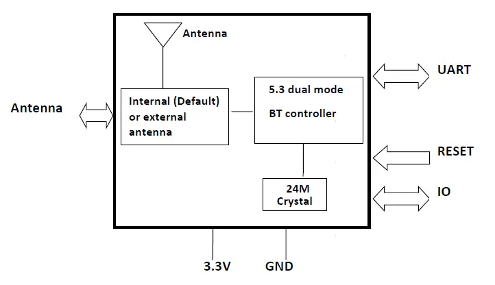
Figure 3-1-1: FSC-BT9104DI Block Diagram 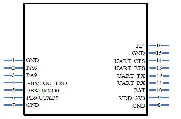
Figure 3-1-2: FSC-BT9104DI PIN Diagram (Top View)
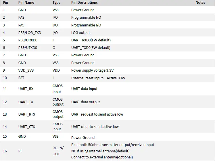
PIN Definition Descriptions
Table 3-2:Pin definition
PHYSICAL INTERFACE
UART Interface\
Table 4-1:Possible UART Settings
| Parameter | Possible Values |
| Minimum – | |
| Baudrate | default 921600bps |
| Flow control | – |
| Parity | None, Odd or Even |
| Number of stop bits | 1 |
| Bits per channel | 8 |
MSL & ESD
Table 5-1: MSL and ESD
| Parameter | Value |
| MSL grade: | MSL 3 |
| ESD grade | Electrostatic discharge |
| ESD – Human-body model (HBM) rating, JESD22-A114-F (Total samples from one wafer lot) | Pass ±2000 V, all pins |
| ESD – Charge-device model (CDM) rating, JESD22-C101-D (Total samples from one wafer lot) | Pass ±500 V, all pins |
RECOMMENDED TEMPERATURE REFLOW PROFILE
Prior to any reflow, it is important to ensure the modules were packaged to prevent moisture absorption. New packages contain desiccate (to absorb moisture) and a humidity indicator card to display the level maintained during storage and shipment. If directed to bake units on the card, please check the below and follow instructions specified by IPC/JEDEC J-STD-033.
Note: The shipping tray cannot be heated above 65°C. If baking is required at the higher temperatures displayed in the below, the modules must be removed from the shipping tray.
Any modules not manufactured before exceeding their floor life should be re-packaged with fresh desiccate and a new humidity indicator card. Floor life for MSL (Moisture Sensitivity Level) 3 devices is 168 hours in ambient environment 30°C/60%RH.
Feasycom module must use Step-Stencil, suggestion using the stencil thickness about 0.16-0.2mm,it could be modify with the product.
Table 6-1: Recommended baking times and temperatures
| MSL | 125°C Baking Temp. | 90°C/≤ 5%RH Baking Temp. | 40°C/ ≤ 5%RH Baking Temp. | |||
| Saturated @ 30°C/85% | Floor Life Limit +72 hours @ 30°C/60% | Saturated @ 30°C/85% | Floor Life Limit +72 hours @ 30°C/60% | Saturated @ 30°C/85% | Floor Life Limit +72 hours @ 30°C/60% | |
| 3 | 9 hours | 7 hours | 33 hours | 23 hours | 13 days | 9 days |
Feasycom surface mount modules are designed to be easily manufactured, including reflow soldering to a PCB. Ultimately it is the responsibility of the customer to choose the appropriate solder paste and to ensure oven temperatures during reflow meet the requirements of the solder paste. Feasycom surface mount modules conform to J-STD-020D1 standards for reflow temperatures.
The soldering profile depends on various parameters necessitating a set up for each application. The data here is given only for guidance on solder reflow.
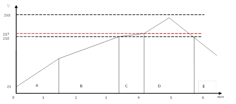
Figure 6-1:Typical Lead-free Re-flow
- Pre-heat zone (A) — This zone raises the temperature at a controlled rate, typically 0.5 – 2 °C/s. The purpose of this zone is to preheat the PCB board and components to 120 ~ 150 °C. This stage is required to distribute the heat uniformly to the PCB board and completely remove solvent to reduce the heat shock to components.
- Equilibrium Zone 1 (B) — In this stage the flux becomes soft and uniformly encapsulates solder particles and spread over PCB board, preventing them from being re-oxidized. Also with elevation of temperature and liquefaction of flux, each activator and rosin get activated and start eliminating oxide film formed on the surface of each solder particle and PCB board. The temperature is recommended to be 150° to 210° for 60 to 120 second for this zone.
- Equilibrium Zone 2 (C) (optional) — In order to resolve the upright component issue, it is recommended to keep the temperature in 210 – 217 ° for about 20 to 30 second.
- Reflow Zone (D) — The profile in the figure is designed for Sn/Ag3.0/Cu0.5. It can be a reference for other lead-free solder. The peak temperature should be high enough to achieve good wetting but not so high as to cause component discoloration or damage. Excessive soldering time can lead to intermetallic growth which can result in a brittle joint. The recommended peak temperature (Tp) is 230 ~ 250 °C. The soldering time should be 30 to 90 second when the temperature is above 217 °C.
- Cooling Zone (E) — The cooling ate should be fast, to keep the solder grains small which will give a longer-lasting joint. Typical cooling rate should be 4 °C.
MECHANICAL DETAILS
Mechanical Details
- Dimension: 10.8mm(W) x 13.5mm(L) x 2.3 mm(H) Tolerance: ±0.2mm
- Module size: 10.8mm X 13.5mm Tolerance: ±0.2mm
- Pad size: 1mmX0.6mm Tolerance: ±0.1mm
- Pad pitch: 1.0mm Tolerance: ±0.1mm
- (Residual plate edge error: < 0.5mm)

Figure 7-1:FSC-BT9104DI footprint Layout Guide (Top View)
HARDWARE INTEGRATION SUGGESTIONS
Soldering Recommendations
The FSC-BT9104DI is compatible with industrial standard reflow profile for Pb-free solders. The reflow profile used is dependent on the thermal mass of the entire populated PCB, heat transfer efficiency of the oven and particular type of solder paste used. Consult the datasheet of particular solder paste for profile configurations.
Feasycom will give following recommendations for soldering the module to ensure reliable solder joint and operation of the module after soldering. Since the profile used is process and layout dependent, the optimum profile should be studied case by case. Thus following recommendation should be taken as a starting point guide.
Layout Guidelines (Internal Antenna)
It is strongly recommended to use good layout practices to ensure proper operation of the module. Placing copper or any metal near antenna deteriorates its operation by having effect on the matching properties. Metal shield around the antenna will prevent the radiation and thus metal case should not be used with the module. Use grounding vias separated max 3 mm apart at the edge of grounding areas to prevent RF penetrating inside the PCB and causing an unintentional resonator. Use GND vias all around the PCB edges.
The mother board should have no bare conductors or vias in this restricted area, because it is not covered by stop mask print. Also no copper (planes, traces or vias) are allowed in this area, because of mismatching the on-board antenna.

Figure 8-2:Restricted Area (Design schematic, for reference only. Unit: mm)
Following recommendations helps to avoid EMC problems arising in the design. Note that each design is unique and the following list do not consider all basic design rules such as avoiding capacitive coupling between signal lines.
Following list is aimed to avoid EMC problems caused by RF part of the module. Use good consideration to avoid problems arising from digital signals in the design.
Ensure that signal lines have return paths as short as possible. For example if a signal goes to an inner layer through a via, always use ground vias around it. Locate them tightly and symmetrically around the signal vias. Routing of any sensitive signals should be done in the inner layers of the PCB. Sensitive traces should have a ground area above and under the line. If this is not possible, make sure that the return path is short by other means (for example using a ground line next to the signal line).
Layout Guidelines (External Antenna)
Placement and PCB layout are critical to optimize the performances of a module without on-board antenna designs. The trace from the antenna port of the module to an external antenna should be 50Ω and must be as short as possible to avoid any interference into the transceiver of the module. The location of the external antenna and RF-IN port of the module should be kept away from any noise sources and digital traces. A matching network might be needed in between the external antenna and RF-IN port to better match the impedance to minimize the return loss.
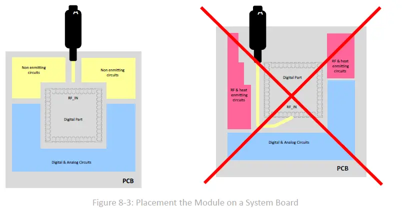
As indicated in below, RF critical circuits of the module should be clearly separated from any digital circuits on the system board. All RF circuits in the module are close to the antenna port. The module, then, should be placed in this way that module digital part towards your digital section of the system PCB.
Antenna Connection and Grounding Plane Design

General design recommendations include
- The length of the trace or connection line should be kept as short as possible.
- Distance between connection and ground area on the top layer should at least be as large as the dielectric thickness.
- Routing the RF close to digital sections of the system board should be avoided.
- To reduce signal reflections, sharp angles in the routing of the micro strip line should be avoided .Chamfers or fillets are preferred for rectangular routing; 45-degree routing is preferred over Manhattanstyle 90-degree routing.

- Routing of the RF-connection underneath the module should be avoided. The distance of the micro stripline to the ground plane on the bottom side of the receiver is very small and has huge tolerances.Therefore, the impedance of this part of the trace cannot be controlled.
- Use as many vias as possible to connect the ground planes.
PRODUCT PACKAGING INFORMATION
Default Packing
Packing box (Optional) 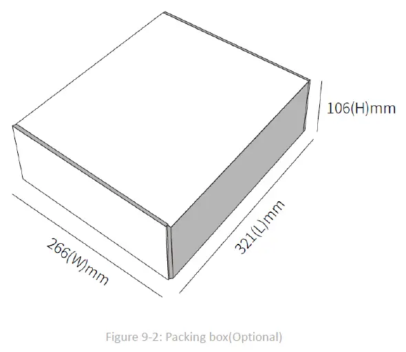
- If other packing is required, please confirm with the customer
- Packing: 1000pcs per carton (Minimum packing quantity)
- The outer packing size is for reference only, please refer to the actual size
APPLICATION SCHEMATIC

FCC Statement BT
FCC Statement
FCCID: 2AMWO-FSCBT9104DI
FCC standards: FCC CFR Title 47 Part 15 Subpart C Section 15.247
Integral antenna with antenna gain 2dBi
This device complies with part 15 of the FCC Rules. Operation is subject to the following two conditions:
- This device may not cause harmful interference, and
- This device must accept any interference received, including interference that may cause undesired operation.
Any Changes or modifications not expressly approved by the party responsible for compliance could void the user’s authority to operate the equipment.
Note: This equipment has been tested and found to comply with the limits for a Class B digital device, pursuant to part 15 of the FCC Rules. These limits are designed to provide reasonable protection against harmful interference in a residential installation. This equipment generates, uses and can radiate radio frequency energy and, if not installed and used in accordance with the instructions, may cause harmful interference to radio communications. However, there is no guarantee that interference will not occur in a particular installation. If this equipment does cause harmful interference to radio or television reception, which can be determined by turning the equipment off and on, the user is encouraged to try to correct the interference by one or more of the following measures:
- Reorient or relocate the receiving antenna.
- Increase the separation between the equipment and receiver.
- Connect the equipment into an outlet on a circuit different from that to which the receiver is connected.
- Consult the dealer or an experienced radio/TV technician for help.
FCC Radiation Exposure Statement
This modular complies with FCC RF radiation exposure limits set forth for an uncontrolled environment. This transmitter must not be co-located or operating in conjunction with any other antenna or transmitter.
If the FCC identification number is not visible when the module is installed inside another device, then the outside of the device into which the module is installed must also display a label referring to the enclosed module. This exterior label can use wording such as the following: “Contains Transmitter Module FCC ID: 2AMWO-FSCBT9104DI Or Contains FCC ID: 2AMWOFSCBT9104DI” When the module is installed inside another device, the user manual of the host must include warning statement as paragraphs A, B and C above.
The devices must be installed and used in strict accordance with the manufacturer’s instructions as described in the user documentation that comes with the product.
Any company of the host device which install this modular with modular approval should perform the test of radiated & conducted emission and spurious emission, etc. according to FCC part 15C : 15.247 and 15.209 & 15.207 ,15B Class B requirement, Only if the test result comply with FCC part 15C : 15.247 and 15.209 & 15.207 ,15B Class B requirement then the host can be sold legally.
FAQ
- Q: What is the default baud rate for the UART interface?
- A: The default baud rate for the UART interface is 921.6k baud.
- Q: Can the module be controlled using ASCII commands?
- A: Yes, the module can be controlled using simple ASCII commands over a serial interface.
Documents / Resources
 |
FEASYCOM FSCBT9104DI Bluetooth Module [pdf] Owner's Manual FSCBT9104DI, FSCBT9104DI Bluetooth Module, Bluetooth Module, Module |


