![]() DG0441
DG0441
Guida Demo
SmartFusion2 SoC FPGA Adaptive FIR Filter – Libero
SoC v11.8 SP1
Guida d'usu
DG0441 SmartFusion2 SoC FPGA Adaptive FIR Filter Libero
Microsemi ùn dà alcuna garanzia, rapprisentazione, o guaranzia in quantu à l'infurmazioni cuntenuti quì o l'adattabilità di i so prudutti è servizii per un scopu particulare, nè Microsemi assume alcuna responsabilità chì deriva da l'applicazione o l'usu di qualsiasi pruduttu o circuitu. I prudutti venduti quì sottu è qualsiasi altri prudutti venduti da Microsemi sò stati sottumessi à una prova limitata è ùn deve micca esse aduprati in cunjunzione cù l'equipaggiu o l'applicazioni critichi per a missione. Ogni specificazione di prestazione hè ritenuta affidabile, ma ùn hè micca verificata, è u Cumpratore deve fà è compie tutte e prestazioni è altre teste di i prudutti, solu è inseme cù, o installati in qualsiasi prudutti finali. L'Acquirente ùn s'appoghjanu micca nantu à e specifiche di dati è di prestazione o parametri furniti da Microsemi. Hè a rispunsabilità di u Cumparatore di determinà indipindentamente l'adattabilità di qualsiasi pruduttu è di pruvà è verificà u listessu. L'infurmazioni furnite da Microsemi quì sottu sò furnite "cum'è, induve hè" è cù tutti i difetti, è tuttu u risicu assuciatu cù tali informazioni hè interamente cù u Cumpratore. Microsemi ùn cuncede, esplicitamente o implicitamente, à alcuna parte alcunu diritti di patenti, licenze, o qualsiasi altri diritti IP, sia in quantu à tali infurmazione stessa o qualcosa descritta da tali informazioni. L'infurmazione furnita in stu documentu hè di proprietà di Microsemi, è Microsemi si riserva u dirittu di fà qualsiasi cambiamenti à l'infurmazioni in stu documentu o à qualsiasi prudutti è servizii in ogni mumentu senza avvisu.
À propositu di Microsemi
Microsemi Corporation (Nasdaq: MSCC) offre una cartera cumpleta di soluzioni di semiconduttori è sistemi per l'aerospaziale è a difesa, a cumunicazione, i centri di dati è i mercati industriali. I prudutti includenu circuiti integrati di signali mixti analogici d'alta prestazione è radiazioni, FPGA, SoC è ASIC; prudutti di gestione di energia; i dispusitivi di timing è di sincronizazione è suluzione di u tempu precisu, chì stabiliscenu u standard di u mondu per u tempu; dispusitivi di trasfurmazioni di voce; suluzione RF; cumpunenti discreti; suluzioni di almacenamento è cumunicazione impresa, tecnulugia di sicurità è anti-t scalabileampi prudutti; suluzioni Ethernet; Power-over-Ethernet IC è midspans; cume capacità è servizii di cuncepimentu persunalizati. Microsemi hà a sede in Aliso Viejo, California, è hà circa 4,800 impiegati in u mondu. Sapete più à www.microsemi.com.
Storia di rivisione
A storia di rivisione descrive i cambiamenti chì sò stati implementati in u documentu. I cambiamenti sò listati per rivisione, cuminciendu cù a publicazione attuale.
1.1 Revisione 7.0
In revision 7.0, the document is updated for Libero v11.8 SP1 software release.
1.2 Revisione 6.0
Aghjurnatu u documentu per a liberazione di u software Libero v11.7.
1.3 Revisione 5.0
Aghjurnatu u documentu per a liberazione di u software Libero v11.6.
1.4 Revisione 4.0
Aghjurnatu u documentu per a liberazione di u software Libero v11.5.
1.5 Revisione 3.0
Aghjurnatu u documentu per a liberazione di u software Libero v11.4.
1.6 Revisione 2.0
The following changes are made in revision 2.0 of this document
- Aghjurnatu u documentu per a liberazione di u software Libero v11.3.
- The Theory of Operation section is updated.
1.7 Revisione 1.0
A rivisione 1.0 hè stata a prima publicazione di stu documentu.
SmartFusion2 SoC FPGA – Adaptive FIR Filter Demo
2.1 Introduzione
The SmartFusion® 2 SoC FPGA devices integrate a fourth generation flash-based FPGA fabric and an ARM Cortex-M3 processor. The SmartFusion2 SoC FPGA fabric includes embedded mathblocks, which are optimized specifically for digital signal processing (DSP) applications such as, finite impulse response (FIR) filters, infinite impulse response (IIR) filters, and fast fourier transform (FFT) functions.
Adaptive filter automatically adjusts the filter coefficients according to the underlying adaptive algorithm and the input signal characteristics. Due to its self adjustment of transfer function of an unknown system and computational requirements, adaptive filters are widely used in different areas of DSP application such as communication, biomedical instrumentation, audio processing, and video processing.
The least mean square (LMS) is a basic adaptive algorithm used in adaptive filters to update the filter coefficients. The LMS algorithm has advantages over other algorithms because of its simplicity, less computations, and best performance in terms of the number of iterations required for convergence.
In this demo, an Adaptive FIR filter application, the suppression of a narrow band signal interference on a wide band signal is implemented using an SmartFusion2 device. Refer to Figure 1, page 2.
The LMS algorithm is implemented in the FPGA fabric to adjust the filter weights/coefficients based on mean square error (MSE) approach. CoreFIR IP is used to perform the filtering operation and CoreFFT IP is used to generate the output spectrum to observe that the narrow band interfering signal component is suppressed. The host interface is implemented in microcontroller subsystem (MSS) to communicate with the Host PC. A user friendly SF2_Adaptive_FIR_Filter.exe generates input signals (narrow band signal and wide band signal), and also plots the input or output waveforms and the required spectrum.

2.2 Teoria di u funziunamentu
Adaptive filters are mainly categorized into four basic architectures:
- Identificazione di u sistema
- Cancellazione di u rumore
- Linear prediction
- Inverse modeling
In this demo, linear prediction architecture is used to implement adaptive filter. The LMS algorithm uses a gradient search technique to determine the filter coefficients that minimize the mean square prediction error. The estimate of the gradient is based on the sample values of the tap-input vector and the error signal. The algorithm iterates over each coefficient in the filter, moving it in the direction of the approximated gradient. After reaching the optimal filter coefficients, the error signal e(n) consists of the wideband signal. The following figure shows the linear prediction based adaptive filter architecture.

The input signal x(n) consists of a desired wideband signal corrupted by narrow band signals that are not required, refer to Figure 3, page 4. In a linear prediction architecture, the desired signal d(n) is same as the input signal x(n) and delayed input x(n-△) is fed to the adaptive filter as shown in Figure 2, page 3.
The delay factor △ (delta) de-correlates the wideband component and correlates the narrow band component of the desired signal d(n) with the delayed input signal x(n-△).
The adaptive filter tries to estimate the narrow band component y(n), and forms an equivalent transfer function, which is similar to that of narrow band filters centered at the frequencies of the narrow band components of the input signal. At the summing junction, the filtered input signal subtracted with delayed input signal produces an error signal. The error signal is used by the LMS algorithm to adjust the filter coefficients. After some iterations, the error signal converges to a wide band component.
The following equations describe computing the coefficients using LMS algorithm.

induve,
According to the above equation, narrowband component y(n), is the adaptive filter output h(n) indicates the filter weights/coefficients x(n-△) is the input signal to adaptive filter
l is length of the filter (number of taps)
k is the index variable.
The error is computed using the following equation:
e(n)= d(n)- y(n)
induve,
e(n) is the error signal
d(n) is desired signal
The filter weights/coefficients are updated using the following equation:
h(n+1)=h(n)+µ*e(n)*x(n-△)
induve,
h(n+1) indicates the estimated filter weights
h(n) is present filter weights
µ is the step size factor
Figure 3 • Input Spectrum of Narrow Band Signal + Wide Band Signal

Figure 4 • Output Spectrum of Wide Band Signal

2.3 Requisiti di Design
Table 1 • Requisiti di Design
| Requisiti di Design | Descrizzione |
| Requisiti Hardware | |
| SmartFusion2 Starter Kit • FlashPro4 programmer • USB A to Mini-B cable |
SF2-484-STARTER-KIT (M2S010-FGG484) |
| Kit di valutazione di sicurezza SmartFusion2 • FlashPro4 programmer • USB A to Mini-B cable |
Rev D or later (M2S090TS-FGG484) |
| Host PC o Laptop | Windows 7, 64-bit Operating System |
| Requisiti di u Software | |
| Libero® System-on-Chip (SoC) | v11.8 SP1 |
| SoftConsole | v 4.0 |
| Software di prugrammazione FlashPro | v11.8 SP1 |
| Drivers di PC Host | Drivers USB à UART |
| Framework | Cliente Microsoft.NET Framework 4 per lanciare GUI demo |
2.4 Demo Design
U disignu files are available for download from the following path in the Microsemi® websitu:
- SmartFusion2 Starter Kit:
http://soc.microsemi.com/download/rsc/?f=m2s_dg0441_starter_liberov11p8_sp1_df - Kit di valutazione di sicurezza SmartFusion2:
http://soc.microsemi.com/download/rsc/?f=m2s_dg0441_eval_liberov11p8_sp1_df
Disegnu files include:
- Disegnu files
- Prugrammazione files
- GUI eseguibile
- Leggimi file
The following figure shows the top-level structure of the SmartFusion2 Starter kit design files. Per più infurmazioni, fate riferimentu à u readme.txt file.
Figure 5 • SmartFusion2 Starter Kit Demo Design Files Struttura di primu livellu

The following figure shows the top-level structure of the SmartFusion2 Security Evaluation kit design files. Per più infurmazioni, fate riferimentu à u readme.txt file.
Figure 6 • SmartFusion2 Security Evaluation Kit Demo Design Files Struttura di primu livellu

2.4.1 Demo Design Description
Stu disignu demo usa i seguenti blocchi:
- MSS block
- Control logic (user RTL)
- LMS_FIR_TOP (Smart Design)
- TPSRAM (IPcore)
- CoreFFT (IPcore)
Figure 7 • Adaptive FIR Filter Demo Block Diagram

2.4.1.1 MSS Block
The MSS block sends and receives the data between the Host PC (GUI interface) and FPGA fabric logic.
The MMUART interface is used to communicate with the Host PC. FIC_0 interface (advanced peripheral bus (APB) master) is used to communicate with the fabric user logic.
2.4.1.2 Lògica di cuntrollu
This is the user logic that is implemented in the fabric and consists of the following two finite-state machines (FSM)s:
- Data Handling: Implements and controls operations like loading the filter input data to the corresponding input data buffer, reading of processed data, and FFT data values. An APB bus slave is implemented to communicate with the MSS APB master.
- Filter Control: Controls the FIR filter and FFT operations. Loads the filtered data to the corresponding output buffer and moves the FFT output data to the corresponding output data buffer.
2.4.1.3 LMS_FIR_TOP
This is a SmartDesign block implemented in the fabric. It consists of the following blocks:
- LMS_CONTROL_FSM: This FSM is implemented in the register-transfer level (RTL) to provide the control signals to the LMS_ALGO block.
- LMS_ALGO: This LMS algorithm is implemented in the RTL to compute the error signal, correction factor, filter coefficients, and to send the filter coefficients to the Core FIR filter.
- CoreFIR: CoreFIR IP is used in the re-loadable coefficient mode to configure its coefficients on the fly. CoreFIR IP configuration is as follows:
- Tipu di filtru: Tariffa unica cumplettamente enumerata
- No of taps: 16
- Coefficients type: Reloadable
- Coefficients bit width: 16 (signed)
- Data bit width: 16 (signed)
- Filter structure: Transposed with no symmetry
2.4.1.4 TPSRAM IP
TPSRAM IP uses the following configurations:
- Input signal data buffer (depth: 1024, width: 16)
- Output signal buffer (depth: 1024, width: 16)
- Output signal FFT real data buffer (depth: 1024, width: 16)
- Output signal FFT imaginary data buffer (depth: 1024, width: 16)
2.4.1.5 CoreFFT
CoreFFT IP is used to generate the frequency spectrum of the filtered data. CoreFFT IP configuration is as follows:
- FFT Architecture: In u locu
- FFT type: Forward
- Scaling FFT: Conditional
- Dimensione di Trasformazione FFT: 256
- Larghezza: 16
For detailed SmartDesign implementation and resource usage summary, refer to Appendix: SmartDesign Implementation, page 25.
2.5 Setting Up the Demo Design for SmartFusion2 Starter Kit
The following steps describe how to setup the hardware demo for SmartFusion2 Starter kit:
- Connect the jumpers on the SmartFusion2 Starter kit board as shown in the following table.
Table 2 • SmartFusion2 Starter Kit Jumper SettingsJumper Cunfigurazione Cumenti JP1 1-2 Close, 3-4 Open Enable power on the M2S-FG484 SOM (VCC3). JP2 1-2 Open, 3-4 Close Select appropriate JTAG è attivate l'alimentazione à u SmartFusion2 JTAG controller. JP3 1-3 Open, 2-4 Close Use the mini-USB port as the power source. - Connect the FlashPro4 programmer to the P5 connector of the SmartFusion2 Starter kit board.
- Connect the Host PC USB port to the P1 Mini USB connector on the SmartFusion2 Starter kit board using the USB Mini-B cable.
The following figure shows the board setup for running the Adaptive FIR filter demo on the SmartFusion2 Starter kit.
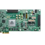
Figure 8 • SmartFusion2 SoC FPGA Starter Kit Setup
- Ensure that the USB to universal asynchronous receiver-transmitter (UART) bridge drivers are automatically detected. This can be verified in the Device Manager of the Host PC.
The following figure shows the USB Serial port.
Figure 9 • USB to UART Bridge Drivers for SmartFusion2 Starter Kit
- Se i driver di u ponte USB à UART ùn sò micca stallati, scaricate è installate i driver da www.microsemi.com/soc/documents/CDM_2.08.24_WHQL_Certified.zip
2.5.1 Setting Up the Demo Design for SmartFusion2 Security Evaluation Kit
The following steps describe how to setup the hardware demo for Security Evaluation kit:
- Connect the jumpers on the SmartFusion2 Security Evaluation kit board as shown in the following table.
Table 3 • Parametri di Jumper di SmartFusion2 Security Evaluation KitJumper Cunfigurazione Cumenti J23 – Jumper to select switch-side multiplexer (MUX) inputs of A or B to the lineside. Chiudi Pin 1-2 (Input A to the lineside) that is on board 125 MHz differential clock oscillator output will be routed to lineside. Apertu Pin 2-3 (Input B to the lineside) that is external clock required to source through SMA connectors to the lineside. J22 – Jumper to select the output enables control for the lineside outputs. Chiudi Pin 1-2 (Lineside output enabled) Apertu Pin 2-3 (Lineside output disabled) J24 Apertu Jumper per furnisce u fornimentu VBUS à USB quandu si usa in u modu Host. J8 – JTAG selection jumper to select between RVI header or FP4 header for application debug. Chiudi Pin 1-2 FP4 for SoftConsole/FlashPro Apertu Pin 2-3 RVI for Keil™ ULINK™/IAR J-Link® Apertu Pin 2-4 for Toggling JTAG_SEL signal remotely using GPIO capability of FT4232 chip. J3 – Jumpers to select either SW2 input or signal ENABLE_FT4232 from FT4232H chip. 1. Ensure that the power supply switch SW7 is OFF while making the jumper connections.
2. Connect the Power supply to the J6 connector, switch on the power supply switch, SW7. - Connect the FlashPro4 programmer to the J5 connector of the SmartFusion2 Security Evaluation kit board.
- Connect the Host PC USB port to the P1 Mini USB connector on the SmartFusion2 Security Evaluation kit board using the USB Mini-B cable.
The following figure shows the board setup for running the DSP Adaptive FIR filter demo on the SmartFusion2 Security Evaluation kit.

- Accende l'interruttore di alimentazione SW7.
- Ensure that the USB to UART bridge drivers are automatically detected. This can be verified in the
Device Manager of the Host PC. The following figure shows the USB Serial port.
- Se i driver di u ponte USB à UART ùn sò micca stallati, scaricate è installate i driver da www.microsemi.com/soc/documents/CDM_2.08.24_WHQL_Certified.zip.
2.6 Programming the Demo Design
The following steps describe how to program the demo design:
Download the demo design from the following links:
- SmartFusion2 Starter Kit: http://soc.microsemi.com/download/rsc/?f=m2s_dg0441_starter_liberov11p8_sp1_df
- Kit di valutazione di sicurezza SmartFusion2: http://soc.microsemi.com/download/rsc/?f=m2s_dg0441_eval_liberov11p8_sp1_df
- Lanciate u software FlashPro.
- Cliccate New Project.
- In the New Project window, enter the project name as SF2_Adaptive_Filter.

- Cliccate Sfoglia è navigate à u locu induve vulete salvà u prugettu.
- Selezziunà un dispusitivu cum'è u modu di prugrammazione.
- Cliccate OK per salvà u prugettu.
2.6.1 Configurazione di u Dispositivu
The following steps describe how to configure the device:
- Click Configure Device on the FlashPro GUI.
- Click Browse and navigate to the location where the Adaptive_FIR_top.stp file si trova è selezziunate u file. The default location of the programming file hè:
• SmartFusion2 Starter Kit: <download_folder>\SF2_Starter_Adaptive_FIR_filter_Demo_DF\Programming files\Adaptive_FIR_top.stp
• SmartFusion2 Security Evaluation Kit: <download_folder>\SF2_Eval_Adaptive_FIR_filter_Demo_DF\Programming files\Adaptive_FIR_top.stp - Cliccate Open. A prugrammazione necessaria file hè sceltu è hè prontu à esse prugrammatu in u dispusitivu.
- Select Advanced as Mode and PROGRAM as Action.
2.6.2 Programming the Device

Click PROGRAM to start programming the device. Wait until programmer status is changed to RUN PASSED as shown in the following figure.

2.6.3 Adaptive FIR Filter Demo GUI
The Adaptive FIR filter demo is provided with a user-friendly GUI that runs on the Host PC and communicates with the SmartFusion2 Starter kit. The UART is used as the underlying communication protocol between the Host PC and SmartFusion2 Starter kit or SmartFusion2 Security Evaluation kit.
The following figure shows the Adaptive FIR filter demo GUI.

The Adaptive FIR filter demo window consists of the following tabs:
- Input Parameters: Configures the serial COM port, filter generation, and signal generation.
- Filter Output: Plots error signal and its frequency spectrum
- Testu Viewer: Shows the coefficients, input signal, output signal, and FFT data values
Click Help for more information on the GUI.
2.7 Esecuzione di u Design
- Launch the Adaptive FIR filter demo GUI, install and invoke the executable file furnitu cù u disignu files. The default location of the executable files sò:
• SmartFusion2 Starter Kit: <download_folder>\SF2_Starter_Adaptive_FIR_filter_Demo_DF\GUI\SF2_Adaptive_FIR_Filter .exe
• SmartFusion2 Security Evaluation Kit: <download_folder>\SF2_Eval_Adaptive_FIR_filter_Demo_DF\GUI\SF2_Adaptive_FIR_Filter.e xe
The Adaptive FIR filter Demo window is displayed, refer to the following figure.
- Serial Port Configuration: The COM port number is automatically detected and baud rate is fixed at 115200. Click Connect. Refer to the preceding figure.
- Signal Generation: Enter the narrowband signal frequency as 2 MHz (supported range is 1 MHz to 20 MHz) and click Generate. Refer to the following figure.
 Adaptive FIR Filter Demo adds the wide band signal (generated inside the Adaptive FIR filter demo window) to the narrow band signal component and plots the combined signal (Narrowband and Wideband), FFT spectrum. Refer to the following figure.
- Click Start to load the input data (1K samples) to the SmartFusion2 device for processing the filtering operation, refer to the following figure.
 After completing the filter operation, the GUI receives the error data and its FFT data from the SmartFusion2 device and plots as shown in the following figure.
The error signal plot shows the suppression of narrowband component from the wideband signal only after the required number of iterations. The narrowband signal component is suppressed gradually in the Error signal frequency spectrum.
This can be observed in the Error signal FFT plot as shown in the following figure.
- Click Compare to analyze the input wide band data with the output wide band data.
 A window displaying the comparison between the input wide band and output wide band is displayed, refer to the following figure.
 The plot can be zoomed in for comparison, refer to the following figure.
- Compare the Error signal (Output wide band signal) with the input wide band signal, refer to the following figure. The narrow band interfering component is eliminated and the wide band signal is preserved in error signal.

- Click Close, refer to the following figure.

- You can copy, save, export, and customize page and configure print setup for the Error Signal plot.
Right-click the Error Signal plot. - From the context sensitive pop-up, select the required option.
It shows the different options as shown in the following figure.
The data can be copied, saved, and exported to CSV plot for analysis purpose.
Page setup, print, show point values, Zoom, and set scale to default are other options for signal analysis.
- The input signal and error signal values can be viewed in the Text Viewer tab. Click the Text Viewer tab and then click the corresponding View mostra in a figura seguente.
 The following figure shows the Text Viewer tab showing the Input Signal values.
- To save the Input Signal as a text file, right-click the Input Signal window. The Input Signal window displays different options as shown in the following figure.
- Click Save. Select OK to save the text file.

- Click Exit to stop the demo, see the following figure.

2.8 Cunclusioni
This demo provides information about the features of the SmartFusion2 device including mathblocks and how to use Microsemi IPs (CoreFIR and CoreFFT) or narrow band interference cancellation application using adaptive filters. This Adaptive FIR filter based-demo is easy to use and provides several options to understand and implement digital signal processing (DSP) filters on the SmartFusion2 device.
Appendix: SmartDesign Implementation
Adaptive FIR filter SmartDesign is shown in the following figure.


The following table shows SmartDesign blocks in Adaptive FIR filter.
Table 4 • Adaptive FIR Filter Demo Smart Design Blocks and Description
| S.No | Block Name | Descrizzione |
| 1 | Adaptive_FIR | FIR_FILTER_0 is a System Builder generated component, in which MMUART is configured to handle the communication between the host PC and fabric logic. To generate a System Builder component, refer to the SmartFusion2 System Builder User Guide. |
| 2 | DATAHANDLE_FSM | Control logic to send/receive the data between MSS and data buffers |
| 3 | FILTERCONTROL_FSM | Control logic to generate the control signals for FIR and FFT operations |
| 4 | LMS_FIR_TOP | SmartDesign |
| 5 | INPUT_Buffer | FIR input signal data buffer |
| OUTPUT_Buffer | FIR output signal buffer | |
| FFT_Im_Buffer | FFT output imaginary data buffer | |
| FFT_Re_Buffer | FFT output real data buffer | |
| 6 | OREFFT | COREFFT |
The following table shows SmartDesign blocks in LMS_FIR_TOP.
Table 5 • LMS_FIR_TOP Smart Design Blocks and Description
| S.No | Block Name | Descrizzione |
| 1 | LMS_ALGO | LMS algorithm implemented in RTL to compute error, correction factor, and filter coefficients. |
| 2 | LMS_CONTROL_FSM | FSM implemented in RTL to control LMS_ALGO block |
| 3 | COREFIR | COREFIR IP |
Appendix: Resource Usage Summary
The following table shows Adaptive FIR filter demo resource usage summary.
Device: SmartFusion2 device
Die: M2S010
Package: 484 FBGA
Table 6 • Adaptive FIR Filter Demo Resource Usage Summary
| Tipu | Adupratu | Totale | Per centutage |
| 4LUT | 2834 | 12084 | 23.45 |
| DFF | 2827 | 12084 | 23.39 |
| RAM 64x18 | 0 | 22 | 0 |
| RAM 1Kx18 | 11 | 21 | 52.38 |
| MACC | 13 | 22 | 59.09 |
The following table shows Adaptive FIR filter resource usage summary.
Device: SmartFusion2 device
Die: M2S090TS
Package: 484 FBGA
Table 7 • Adaptive FIR Filter Demo Resource Usage Summary
| Tipu | Adupratu | Totale | Per centutage |
| 4LUT | 2833 | 86184 | 3.29 |
| DFF | 2827 | 86184 | 3.28 |
| RAM 64x18 | 0 | 112 | 0 |
| RAM 1K18 | 11 | 109 | 10.09 |
| MACC | 13 | 84 | 15.48 |
The following table shows MACC blocks usage summary.
Table 8 • MACC Blocks Usage Summary
| CoreFIR | CoreFFT | LMS_ALGO | Totale |
| 8 | 04 | 1 | 13 |
![]()
Sede centrale di Microsemi
One Enterprise, Aliso Viejo,
CA 92656 USA
In i Stati Uniti: +1 800-713-4113
Fora di i Stati Uniti: +1 949-380-6100
Fax: +1 949-215-4996
E-mail: sales.support@microsemi.com
www.microsemi.com
© 2017 Microsemi Corporation. Tutti i diritti riservati. Microsemi è u logo Microsemi sò marchi di Microsemi Corporation. Tutti l'altri marchi è marchi di serviziu sò a pruprietà di i so rispettivi pruprietarii.
Documenti / Risorse
 |
Microsemi DG0441 SmartFusion2 SoC FPGA Adaptive FIR Filter Libero [pdfGuida di l'utente DG0441 SmartFusion2 SoC FPGA Adaptive FIR Filter Libero, DG0441, SmartFusion2 SoC FPGA Adaptive FIR Filter Libero, FIR Filter Libero |