![]() Kintex-7 FPGA
Kintex-7 FPGA
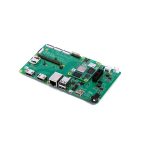
Core Board
AC7K325B
User Manual
Version Record
| Version | Date | Release By | Description |
| Rev 1.0 | 2020-06-28 | Rachel Zhou | First Release |
Part 1: AC7K325B Core Board Introduction
AC7K325B (core board model, the same below) FPGA core board, it is based on XILINX Kintex-7 XC7K325 series chip XC7K325TFFG900100T. The core board uses 4 Micron’s 512MB DDR3 chips MT41J256M16HA-125, with a total capacity of 2GB. In addition, a 128MBit QSPI FLASH is also integrated on the core board for boot storage configuration and system files.
The four board-to-board connectors of the core board AC7K325B expand 276 IOs, of which 92 IO levels of BANK17 and BANK18 can be modified by replacing the LDO chip on the core board to meet the user’s requirement of no level interface; In addition, the core board also extended 16 pairs of high-speed transceiver GTX interfaces. For users who need a lot of IO, this core board will be a good choice. And the IO connection part, the FPGA chip to the interface between the equal length and differential processing, and the core board size is only 80 * 60 (mm), very suitable for secondary development.

Part 2: FPGA Chip
As mentioned above, the FPGA model we use is XC7K325T-2FFG900I, which belongs to Xilinx’s KINTEX-7 series. The speed grade is 2, and the temperature grade is industry grade. This model is a FGG900 package with 900 pins. Xilinx KINTEX-7 FPGA chip naming rules as below 
The main parameters of the FPGA chip XC7K325T are as follows
| Name | Specific parameters |
| Logic Cells | 326,080 |
| Slices | 50,950 |
| CLB flip-flops | 407,600 |
| Block RAM(kb) | 16,020 |
| DSP Slices | 840 |
| PCIe Gen2 | 1 |
| XADC | 1 XADC, 12bit, 1Mbps AD |
| GTP Transceiver | 16 GTP, 12.5Gb/s max |
| Speed Grade | -2 |
| Temperature Grade | Industrial |
Part 3: DDR3 DRAM
The FPGA core board AC7K325B is equipped with four Micron 4Gbit (512MB) DDR3 chips, model MT41J256M16HA-125 (compatible with MT41K256M16HA-125). Four DDR3 SDRAMs make up a 64-bit bus width. Because 4 DDR3 chips are connected to the HP port of the FPGA, the maximum operating speed of DDR3 SDRAM can reach 800MHz (data rate 1600Mbps). Four DDR3 memory systems are directly connected to the BANK32, BANK33, and BANK34 interfaces of the FPGA. The specific configuration of DDR3 SDRAM is shown in Table 3-1 below.
| Bit Number | Chip Model | Capacity | Factory |
| U4,U5, U6, U7 | MT41K256M16HA-125 or MT41J256M16HA-125 |
256M x 16bit | Micron |
Table 3-1: DDR3 SDRAM Configuration
The hardware design of DDR3 requires strict consideration of signal integrity. We have fully considered the matching resistor/terminal resistance, trace impedance control, and trace length control in circuit design and PCB design to ensure high-speed and stable operation of DDR3.
DDR3 DRAM pin assignment:
| Net Name | FPGA PIN Name | FPGA P/N |
| DDR3_D0 | IO_L13P_T2_MRCC_32 | AD18 |
| DDR3_D1 | IO_L16N_T2_32 | AB18 |
| DDR3_D2 | IO_L14P_T2_SRCC_32 | AD17 |
| DDR3_D3 | IO_L17P_T2_32 | AB19 |
| DDR3_D4 | IO_L14N_T2_SRCC_32 | AD16 |
| DDR3_D5 | IO_L17N_T2_32 | AC19 |
| DDR3_D6 | IO_L13N_T2_MRCC_32 | AE18 |
| DDR3_D7 | IO_L18P_T2_32 | AB17 |
| DDR3_D8 | IO_L8P_T1_32 | AG19 |
| DDR3_D9 | IO_L7N_T1_32 | AK19 |
| DDR3_D10 | IO_L10P_T1_32 | AD19 |
| DDR3_D11 | IO_L7P_T1_32 | AJ19 |
| DDR3_D12 | IO_L11P_T1_SRCC_32 | AF18 |
| DDR3_D13 | IO_L8N_T1_32 | AH19 |
| DDR3_D14 | IO_L10N_T1_32 | AE19 |
| DDR3_D15 | IO_L11N_T1_SRCC_32 | AG18 |
| DDR3_D16 | IO_L1N_T0_32 | AK15 |
| DDR3_D17 | IO_L5N_T0_32 | AJ17 |
| DDR3_D18 | IO_L2N_T0_32 | AH15 |
| DDR3_D19 | IO_L4P_T0_32 | AF15 |
| DDR3_D20 | IO_L4N_T0_32 | AG14 |
| DDR3_D21 | IO_L5P_T0_32 | AH17 |
| DDR3_D22 | IO_L2P_T0_32 | AG15 |
| DDR3_D23 | IO_L1P_T0_32 | AK16 |
| DDR3_D24 | IO_L19P_T3_32 | AE15 |
| DDR3_D25 | IO_L24P_T3_32 | Y16 |
| DDR3_D26 | IO_L22P_T3_32 | AC14 |
| DDR3_D27 | IO_L20P_T3_32 | AA15 |
| DDR3_D28 | IO_L23P_T3_32 | AA17 |
| DDR3_D29 | IO_L22N_T3_32 | AD14 |
| DDR3_D30 | IO_L23N_T3_32 | AA16 |
| DDR3_D31 | IO_L20N_T3_32 | AB15 |
| DDR3_D32 | IO_L22N_T3_34 | AK6 |
| DDR3_D33 | IO_L23P_T3_34 | AJ8 |
| DDR3_D34 | IO_L22P_T3_34 | AJ6 |
| DDR3_D35 | IO_L19P_T3_34 | AF8 |
| DDR3_D36 | IO_L24N_T3_34 | AK4 |
| DDR3_D37 | IO_L23N_T3_34 | AK8 |
| DDR3_D38 | IO_L24P_T3_34 | AK5 |
| DDR3_D39 | IO_L20N_T3_34 | AG7 |
| DDR3_D40 | IO_L10P_T1_34 | AE4 |
| DDR3_D41 | IO_L8N_T1_34 | AF1 |
| DDR3_D42 | IO_L11P_T1_SRCC_34 | AE5 |
| DDR3_D43 | IO_L8P_T1_34 | AE1 |
| DDR3_D44 | IO_L12P_T1_MRCC_34 | AF6 |
| DDR3_D45 | IO_L10N_T1_34 | AE3 |
| DDR3_D46 | IO_L11N_T1_SRCC_34 | AF5 |
| DDR3_D47 | IO_L7N_T1_34 | AF2 |
| DDR3_D48 | IO_L13P_T2_MRCC_34 | AH4 |
| DDR3_D49 | IO_L16N_T2_34 | AJ2 |
| DDR3_D50 | IO_L14N_T2_SRCC_34 | AH5 |
| DDR3_D51 | IO_L13N_T2_MRCC_34 | AJ4 |
| DDR3_D52 | IO_L16P_T2_34 | AH2 |
| DDR3_D53 | IO_L17N_T2_34 | AK1 |
| DDR3_D54 | IO_L14P_T2_SRCC_34 | AH6 |
| DDR3_D55 | IO_L17P_T2_34 | AJ1 |
| DDR3_D56 | IO_L2P_T0_34 | AC2 |
| DDR3_D57 | IO_L4P_T0_34 | AC5 |
| DDR3_D58 | IO_L1N_T0_34 | AD3 |
| DDR3_D59 | IO_L6P_T0_34 | AC7 |
| DDR3_D60 | IO_L5N_T0_34 | AE6 |
| DDR3_D61 | IO_L5P_T0_34 | AD6 |
| DDR3_D62 | IO_L2N_T0_34 | AC1 |
| DDR3_D63 | IO_L4N_T0_34 | AC4 |
| DDR3_DM0 | IO_L16P_T2_32 | AA18 |
| DDR3_DM1 | IO_L12P_T1_MRCC_32 | AF17 |
| DDR3_DM2 | IO_L6P_T0_32 | AE16 |
| DDR3_DM3 | IO_L24N_T3_32 | Y15 |
| DDR3_DM4 | IO_L20P_T3_34 | AF7 |
| DDR3_DM5 | IO_L7P_T1_34 | AF3 |
| DDR3_DM6 | IO_L18P_T2_34 | AJ3 |
| DDR3_DM7 | IO_L1P_T0_34 | AD4 |
| DDR3_DQS0_P | IO_L15P_T2_DQS_32 | Y19 |
| DDR3_DQS0_N | IO_L15N_T2_DQS_32 | Y18 |
| DDR3_DQS1_P | IO_L9P_T1_DQS_32 | AJ18 |
| DDR3_DQS1_N | IO_L9N_T1_DQS_32 | AK18 |
| DDR3_DQS2_P | IO_L3P_T0_DQS_32 | AH16 |
| DDR3_DQS2_N | IO_L3N_T0_DQS_32 | AJ16 |
| DDR3_DQS3_P | IO_L21P_T3_DQS_32 | AC16 |
| DDR3_DQS6_N | IO_L15N_T2_DQS_34 | AH1 |
| DDR3_DQS7_P | IO_L3P_T0_DQS_34 | AD2 |
| DDR3_DQS7_N | IO_L3N_T0_DQS_34 | AD1 |
| DDR3_A0 | IO_L1P_T0_33 | AA12 |
| DDR3_A1 | IO_L1N_T0_33 | AB12 |
| DDR3_A2 | IO_L2P_T0_33 | AA8 |
| DDR3_A3 | IO_L2N_T0_33 | AB8 |
| DDR3_A4 | IO_L3P_T0_DQS_33 | AB9 |
| DDR3_A5 | IO_L3N_T0_DQS_33 | AC9 |
| DDR3_A6 | IO_L6N_T0_VREF_33 | AB13 |
| DDR3_A7 | IO_L4N_T0_33 | Y10 |
| DDR3_A8 | IO_L5P_T0_33 | AA11 |
| DDR3_A9 | IO_L5N_T0_33 | AA10 |
| DDR3_A10 | IO_L6P_T0_33 | AA13 |
| DDR3_A11 | IO_L8P_T1_33 | AD8 |
| DDR3_A12 | IO_L7P_T1_33 | AB10 |
| DDR3_A13 | IO_L7N_T1_33 | AC10 |
| DDR3_A14 | IO_L15P_T2_DQS_33 | AJ9 |
| DDR3_BA0 | IO_L8N_T1_33 | AE8 |
| DDR3_BA1 | IO_L9P_T1_DQS_33 | AC12 |
| DDR3_BA2 | IO_L9N_T1_DQS_33 | AC11 |
| DDR3_WE | IO_L10P_T1_33 | AD9 |
| DDR3_RAS | IO_L10N_T1_33 | AE9 |
| DDR3_CAS | IO_L11P_T1_SRCC_33 | AE11 |
| DDR3_S0 | IO_L11N_T1_SRCC_33 | AF11 |
| DDR3_CKE0 | IO_L12P_T1_MRCC_33 | AD12 |
| DDR3_ODT | IO_L12N_T1_MRCC_33 | AD11 |
| DDR3_CLK0_P | IO_L13P_T2_MRCC_33 | AG10 |
| DDR3_CLK0_N | IO_L13N_T2_MRCC_33 | AH10 |
| DDR3_RESET | IO_L4P_T0_33 | Y11 |
Part 4: QSPI Flash
The FPGA core board AX7K325 is equipped with one 128MBit QSPI FLASH, and the model is W25Q128A, which uses the 3.3V CMOS voltage standard. Due to the non-volatile nature of QSPI FLASH, it can be used as a boot device for the system to store the boot image of the system. The specific models and related parameters of QSPI FLASH are shown in Table 4-1.
| Position | Model | Capacity | Factory |
| U14 | N25Q128 | 128M Bit | Numonyx |
Table 4-1: QSPI FLASH Specification
QSPI FLASH is connected to the dedicated pins of BANK0 and BANK14 of the FPGA chip. The clock pin is connected to CCLK0 of BANK0, and other data and chip select signals are connected to D00~D03 and FCS pin of BANK14 respectively. Figure 4-1 shows the hardware connection of QSPI Flash.
QSPI Flash pin assignments:
| Net Name | FPGA PIN Name | FPGA P/N |
| FPGA_CCLK | CCLK_0 | B10 |
| FLASH_CE_B | IO_L6P_T0_FCS_B_14 | U19 |
| FLASH_D0 | IO_L1P_T0_D00_MOSI_14 | P24 |
| FLASH_D1 | IO_L1N_T0_D01_DIN_14 | R25 |
| FLASH_D2 | IO_L2P_T0_D02_14 | R20 |
| FLASH_D3 | IO_L2N_T0_D03_14 | R21 |
Part 5: Clock Configuration
The AC7K325B core board is equipped with two Sitime active differential crystals, one is 200MHz, the model is SiT9102-200.00MHz, the system main clock for FPGA and used to generate DDR3 control clock; the other is 125MHz, model is SiT9102 -125MHz, reference clock input for GTP transceivers.
Part 5.1: 200Mhz Active Differential clock
G1 in Figure 5-2 is the 200M active differential crystal that provides the development board system clock source. The crystal output is connected to the BANK33 global clock pin MRCC of the FPGA. This 200Mhz differential clock can be used to drive the DDR3 controller and user logic in the FPGA.

200Mhz Differential Clock Pin Assignment
| Signal Name | FPGA PIN |
| SYS_CLK_P | AE10 |
| SYS_CLK_N | AF10 |
Part 5.2: GTX Reference Clock
G2 in Figure 5-3 is the 125Mhz active differential crystal. The reference clock is connected to the reference clock input REFCLK1P / REFCLK1N of BANK117. The schematic diagram of this clock source is shown in Figure 5-3
GTX Reference Clock
| Net Name | FPGA PIN |
| BANK117_CLK1_P | J8 |
| BANK117_CLK1_N | J7 |
Part 6: LED Light on Core Board
There are 2 red LED lights on the AC7K325B FPGA core board, one of which is the power indicator light (PWR), one is the configuration LED light (DONE). When the core board is powered, the power indicator will illuminate; when the FPGA is configured, the configuration LED will illuminate. The schematic diagram of the LED light hardware connection is shown in Figure 6-1:
Part 7: Power Supply
The power supply voltage of AC7K325B core board is DC5V, which is supplied by connecting the carrier board. The schematic diagram of the power supply design on the core board is shown in Figure 7-1 below:
+ 5V generates + 1.0V FPGA core power through the DCDC power chip MYMGK1R820FRSR. The output current of the MYMGK1R820FRSR is as high as 20A, which far meets the core voltage current demand. The + 5V power is generated by the DCDC chip ETA1471 to generate four power sources: + 1.5V, + 3.3V, +1.8V,+ 1.5V and MGTAVTT. The + 1.0V used by the GTX transceiver is generated by the DCDC chip ETA8156. The GTX auxiliary power + 1.8V through an LDO chip SPX3819-1-8. The VTT and VREF voltages for DDR3 are generated by the TPS51200. In addition, two SPX3819M5-3-3 are used to generate the IO power of BANK17 and BANK18. Users can change the LDO chip to make the IO input and output of these two banks to other voltage standards.
Because the power supply of the FPGA requires the power-on sequence, in the circuit design, according to the power requirements of the chip, the power-on sequence is + 1.0V-> + 1.8V-> (+ 1.5 V, + 3.3V, VCCIO17, VCCIO18, Ensure that the chip works properly.
Part 8: Size Dimension

Part 9: Board to Board Connectors pin assignment
The core board expands a total of four high-speed expansion connectors, and uses four 120-Pin inter-board connectors (J29 ~ J32) to connect to the carrier board. The connector uses Panasonic’s AXK5A2137YG. Among them, J29 is connected to the GTX transceiver signal, J30 is connected to the JTAG, and the IOs of BANK17 and BANK18, J31 is connected to the IO of BANK15 and BANK16, J32 is connected to the IO of BANK12 and BANK13 and + 5V power.
Pin assignment of J29 connector
| J29 Pin | Signal Name | FPGA Pin | J29 Pin | Signal Name | FPGA Pin |
| 1 | BANK115_TX0_N | Y1 | 2 | BANK115_RX0_N | AA3 |
| 3 | BANK115_TX0_P | Y2 | 4 | BANK115_RX0_P | AA4 |
| 5 | GND | – | 6 | GND | – |
| 7 | BANK115_TX1_N | V1 | 8 | BANK115_RX1_N | Y5 |
| 9 | BANK115_TX1_P | V2 | 10 | BANK115_RX1_P | Y6 |
| 11 | GND | – | 12 | GND | – |
| 13 | BANK115_TX2_N | U3 | 14 | BANK115_RX2_N | W3 |
| 15 | BANK115_TX2_P | U4 | 16 | BANK115_RX2_P | W4 |
| 17 | GND | – | 18 | GND | – |
| 19 | BANK115_TX3_N | T1 | 20 | BANK115_RX3_N | V5 |
| 21 | BANK115_TX3_P | T2 | 22 | BANK115_RX3_P | V6 |
| 23 | GND | – | 24 | GND | – |
| 25 | BANK115_CLK0_N | R7 | 26 | BANK115_CLK1_N | U7 |
| 27 | BANK115_CLK0_P | R8 | 28 | BANK115_CLK1_N | U8 |
| 29 | GND | – | 30 | GND | – |
| 31 | BANK116_TX0_N | P1 | 32 | BANK116_RX0_N | T5 |
| 33 | BANK116_TX0_P | P2 | 34 | BANK116_RX0_P | T6 |
| 35 | GND | – | 36 | GND | – |
| 37 | BANK116_TX1_N | N3 | 38 | BANK116_RX1_N | R3 |
| 39 | BANK116_TX1_P | N4 | 40 | BANK116_RX1_P | R4 |
| 41 | GND | – | 42 | GND | – |
| 43 | BANK116_TX2_N | M1 | 44 | BANK116_RX2_N | P5 |
| 45 | BANK116_TX2_P | M2 | 46 | BANK116_RX2_P | P6 |
| 47 | GND | – | 48 | GND | – |
| 49 | BANK116_TX3_N | L3 | 50 | BANK116_RX3_N | M5 |
| 51 | BANK116_TX3_P | L4 | 52 | BANK116_RX3_P | M6 |
| 53 | GND | – | 54 | GND | – |
| 55 | BANK116_CLK0_N | L7 | 56 | BANK116_CLK1_N | N7 |
| 57 | BANK116_CLK0_P | L8 | 58 | BANK116_CLK1_P | N8 |
| 59 | GND | – | 60 | GND | – |
| 61 | BANK117_TX0_N | K1 | 62 | BANK118_TX0_N | D1 |
| 63 | BANK117_TX0_P | K2 | 64 | BANK118_TX0_P | D2 |
| 65 | GND | – | 66 | GND | – |
| 67 | BANK117_RX0_N | K5 | 68 | BANK118_RX0_N | E3 |
| 69 | BANK117_RX0_P | K6 | 70 | BANK118_RX0_P | E4 |
| 71 | GND | – | 72 | GND | – |
| 73 | BANK117_TX1_N | J3 | 74 | BANK118_TX1_N | C3 |
| 75 | BANK117_TX1_P | J4 | 76 | BANK118_TX1_P | C4 |
| 77 | GND | – | 78 | GND | – |
| 79 | BANK117_RX1_N | H5 | 80 | BANK118_RX1_N | D5 |
| 81 | BANK117_RX1_P | H6 | 82 | BANK118_RX1_P | D6 |
| 83 | GND | – | 84 | GND | – |
| 85 | BANK117_TX2_N | H1 | 86 | BANK118_TX2_N | B1 |
| 87 | BANK117_TX2_P | H2 | 88 | BANK118_TX2_P | B2 |
| 89 | GND | – | 90 | GND | – |
| 91 | BANK117_RX2_N | G3 | 92 | BANK118_RX2_N | B5 |
| 93 | BANK117_RX2_P | G4 | 94 | BANK118_RX2_P | B6 |
| 95 | GND | – | 96 | GND | – |
| 97 | BANK117_TX3_N | F1 | 98 | BANK118_TX3_N | A3 |
| 99 | BANK117_TX3_P | F2 | 100 | BANK118_TX3_P | A4 |
| 101 | GND | – | 102 | GND | – |
| 103 | BANK117_RX3_N | F5 | 104 | BANK118_RX3_N | A7 |
| 105 | BANK117_RX3_P | F6 | 106 | BANK118_RX3_P | A8 |
| 107 | GND | – | 108 | GND | – |
| 109 | BANK117_CLK0_N | G7 | 110 | BANK118_CLK0_N | C7 |
| 111 | BANK117_CLK0_P | G8 | 112 | BANK118_CLK0_P | C8 |
| 113 | GND | – | 114 | GND | – |
| 115 | 116 | BANK118_CLK1_N | E7 | ||
| 117 | 118 | ||||
| 119 | GND | – | 120 | GND | – |
Pin assignment of J30 connector
| J30 Pin | Signal Name | FPGA Pin | J30 Pin | Signal Name | FPGA Pin |
| 1 | B18_L5_P | K14 | 2 | B18_L3_P | L12 |
| 3 | B18_L5_N | J14 | 4 | B18_L3_N | L13 |
| 5 | B18_L6_P | L11 | 6 | B18_L2_P | L15 |
| 7 | B18_L6_N | K11 | 8 | B18_L2_N | K15 |
| 9 | GND | – | 10 | GND | – |
| 11 | B18_L7_P | H15 | 12 | B18_L1_P | L16 |
| 13 | B18_L7_N | G15 | 14 | B18_L1_N | K16 |
| 15 | B18_L8_P | J11 | 16 | B18_L4_P | K13 |
| 17 | B18_L8_N | J12 | 18 | B18_L4_N | J13 |
| 19 | GND | – | 20 | GND | – |
| 21 | B18_L9_P | J16 | 22 | B18_L12_P | G13 |
| 23 | B18_L9_N | H16 | 24 | B18_L12_N | F13 |
| 25 | B18_L16_P | F11 | 26 | B18_L10_P | H11 |
| 27 | B18_L16_N | E11 | 28 | B18_L10_N | H12 |
| 29 | GND | – | 30 | GND | – |
| 31 | B18_L18_P | D11 | 32 | B18_L20_P | E14 |
| 33 | B18_L18_N | C11 | 34 | B18_L20_N | E15 |
| 35 | B18_L15_P | C12 | 36 | B18_L11_P | H14 |
| 37 | B18_L15_N | B12 | 38 | B18_L11_N | G14 |
| 39 | GND | – | 40 | GND | – |
| 41 | B18_L23_P | C15 | 42 | B18_L21_P | D14 |
| 43 | B18_L23_N | B15 | 44 | B18_L21_N | C14 |
| 45 | B18_L17_P | A11 | 46 | B18_L22_P | B13 |
| 47 | B18_L17_N | A12 | 48 | B18_L22_N | A13 |
| 49 | GND | – | 50 | GND | – |
| 51 | B18_L24_P | B14 | 52 | B17_L5_N | L18 |
| 53 | B18_L24_N | A15 | 54 | B17_L5_P | L17 |
| 55 | B18_L19_P | F15 | 56 | B17_L15_P | D16 |
| 57 | B18_L19_N | E16 | 58 | B17_L15_N | C16 |
| 59 | GND | – | 60 | GND | – |
| 61 | B17_L17_P | C17 | 62 | B17_L14_P | E19 |
| 63 | B17_L17_N | B17 | 64 | B17_L14_N | D19 |
| 65 | B17_L1_P | K18 | 66 | B17_L20_P | A16 |
| 67 | B17_L1_N | J18 | 68 | B17_L20_N | A17 |
| 69 | GND | – | 70 | GND | – |
| 71 | B17_L22_N | A18 | 72 | B17_L21_P | A20 |
| 73 | B17_L22_P | B18 | 74 | B17_L21_N | A21 |
| 75 | B17_L8_P | D21 | 76 | B17_L13_P | D17 |
| 77 | B17_L8_N | C21 | 78 | B17_L13_N | D18 |
| 79 | GND | – | 80 | GND | – |
| 81 | B17_L24_P | C19 | 82 | B17_L23_N | A22 |
| 83 | B17_L24_N | B19 | 84 | B17_L23_P | B22 |
| 85 | B17_L18_N | F17 | 86 | B17_L12_P | F20 |
| 87 | B17_L18_P | G17 | 88 | B17_L12_N | E20 |
| 89 | GND | – | 90 | GND | – |
| 91 | B17_L19_N | B20 | 92 | B17_L11_N | E21 |
| 93 | B17_L19_P | C20 | 94 | B17_L11_P | F21 |
| 95 | B17_L10_N | C22 | 96 | B17_L9_N | F22 |
| 97 | B17_L10_P | D22 | 98 | B17_L9_P | G22 |
| 99 | GND | – | 100 | GND | – |
| 101 | B17_L16_N | F18 | 102 | B17_L7_P | H21 |
| 103 | B17_L16_P | G18 | 104 | B17_L7_N | H22 |
| 105 | B17_L2_N | G20 | 106 | B17_L3_N | H17 |
| 107 | B17_L2_P | H20 | 108 | B17_L3_P | J17 |
| 109 | GND | – | 110 | GND | – |
| 111 | B17_L4_N | H19 | 112 | FPGA_TCK | E10 |
| 113 | B17_L4_P | J19 | 114 | FPGA_TMS | F10 |
| 115 | B17_L6_P | K19 | 116 | FPGA_TDO | G10 |
| 117 | B17_L6_N | K20 | 118 | FPGA_TDI | H10 |
| 119 | GND | – | 120 | GND | – |
Pin assignment of J31 connector
| J31 Pin | Signal Name | FPGA Pin | J31 Pin | Signal Name | FPGA Pin |
| 1 | B16_L12_N | B25 | 2 | B16_L8_P | C24 |
| 3 | B16_L12_P | C25 | 4 | B16_L8_N | B24 |
| 5 | B16_L10_N | A26 | 6 | B16_L16_N | C30 |
| 7 | B16_L10_P | A25 | 8 | B16_L16_P | D29 |
| 9 | GND | – | 10 | GND | – |
| 11 | B16_L11_N | C26 | 12 | B16_L7_N | A27 |
| 13 | B16_L11_P | D26 | 14 | B16_L7_P | B27 |
| 15 | B16_L13_N | C27 | 16 | B16_L18_N | E30 |
| 17 | B16_L13_P | D27 | 18 | B16_L18_P | E29 |
| 19 | GND | – | 20 | GND | – |
| 21 | B16_L21_P | G27 | 22 | B16_L14_N | D28 |
| 23 | B16_L21_N | F27 | 24 | B16_L14_P | E28 |
| 25 | B16_L20_N | F28 | 26 | B16_L22_N | F30 |
| 27 | B16_L20_P | G28 | 28 | B16_L22_P | G29 |
| 29 | GND | – | 30 | GND | – |
| 31 | B16_L9_P | B28 | 32 | B16_L5_P | F26 |
| 33 | B16_L9_N | A28 | 34 | B16_L5_N | E26 |
| 35 | B16_L15_P | C29 | 36 | B16_L24_N | G30 |
| 37 | B16_L15_N | B29 | 38 | B16_L24_P | H30 |
| 39 | GND | – | 40 | GND | – |
| 41 | B16_L19_N | H25 | 42 | B16_L23_N | H27 |
| 43 | B16_L19_P | H24 | 44 | B16_L23_P | H26 |
| 45 | B16_L1_N | A23 | 46 | B16_L17_P | B30 |
| 47 | B16_L1_P | B23 | 48 | B16_L17_N | A30 |
| 49 | GND | – | 50 | GND | – |
| 51 | B16_L2_P | E23 | 52 | B16_L3_N | E25 |
| 53 | B16_L2_N | D23 | 54 | B16_L3_P | F25 |
| 55 | B16_L6_N | G24 | 56 | B16_L4_P | E24 |
| 57 | B16_L6_P | G23 | 58 | B16_L4_N | D24 |
| 59 | GND | – | 60 | GND | – |
| 61 | B15_L14_N | L28 | 62 | B15_L7_N | H29 |
| 63 | B15_L14_P | M28 | 64 | B15_L7_P | J29 |
| 65 | B15_L10_N | J26 | 66 | B15_L8_N | J28 |
| 67 | B15_L10_P | K26 | 68 | B15_L8_P | J27 |
| 69 | GND | – | 70 | GND | – |
| 71 | B15_L1_N | J24 | 72 | B15_L24_N | M23 |
| 73 | B15_L1_P | J23 | 74 | B15_L24_P | M22 |
| 75 | B15_L18_N | N26 | 76 | B15_L3_N | K24 |
| 77 | B15_L18_P | N25 | 78 | B15_L3_P | K23 |
| 79 | GND | – | 80 | GND | – |
| 81 | B15_L2_N | L23 | 82 | B15_L21_N | N24 |
| 83 | B15_L2_P | L22 | 84 | B15_L21_P | P23 |
| 85 | B15_L13_P | K28 | 86 | B15_L12_N | K25 |
| 87 | B15_L13_N | K29 | 88 | B15_L12_P | L25 |
| 89 | GND | – | 90 | GND | – |
| 91 | B15_L22_N | P22 | 92 | B15_L20_N | N22 |
| 93 | B15_L22_P | P21 | 94 | B15_L20_P | N21 |
| 95 | B15_L15_N | M30 | 96 | B15_L9_N | K30 |
| 97 | B15_L15_P | M29 | 98 | B15_L9_P | L30 |
| 99 | GND | – | 100 | GND | – |
| 101 | B15_L19_N | N20 | 102 | B15_L5_N | J22 |
| 103 | B15_L19_P | N19 | 104 | B15_L5_P | J21 |
| 105 | B15_L17_N | N30 | 106 | B15_L6_N | L20 |
| 107 | B15_L17_P | N29 | 108 | B15_L6_P | M20 |
| 109 | GND | – | 110 | GND | – |
| 111 | B15_L11_N | L27 | 112 | B15_L16_N | M27 |
| 113 | B15_L11_P | L26 | 114 | B15_L16_P | N27 |
| 115 | B15_L23_N | M25 | 116 | B15_L4_P | L21 |
| 117 | B15_L23_P | M24 | 118 | B15_L4_N | K21 |
| 119 | GND | – | 120 | GND | – |
Pin assignment of J32 connector
| J32 Pin | Signal Name | FPGA Pin | J32 Pin | Signal Name | FPGA Pin |
| 1 | B13_L16_P | AE30 | 2 | B13_L10_N | AB30 |
| 3 | B13_L16_N | AF30 | 4 | B13_L10_P | AB29 |
| 5 | B13_L23_N | AF27 | 6 | B13_L9_P | AD29 |
| 7 | B13_L23_P | AF26 | 8 | B13_L9_N | AE29 |
| 9 | GND | U14 | 10 | GND | U14 |
| 11 | B13_L14_P | AE28 | 12 | B13_L6_P | AA25 |
| 13 | B13_L14_N | AF28 | 14 | B13_L6_N | AB25 |
| 15 | B13_L13_P | AG29 | 16 | B13_L5_N | AB28 |
| 17 | B13_L13_N | AH29 | 18 | B13_L5_P | AA27 |
| 19 | GND | U14 | 20 | GND | U14 |
| 21 | B13_L18_P | AG30 | 22 | B13_L2_N | W28 |
| 23 | B13_L18_N | AH30 | 24 | B13_L2_P | W27 |
| 25 | B13_L21_N | AG28 | 26 | B13_L8_P | Y30 |
| 27 | B13_L21_P | AG27 | 28 | B13_L8_N | AA30 |
| 29 | GND | U14 | 30 | GND | U14 |
| 31 | B13_L15_N | AK30 | 32 | B13_L11_N | AD28 |
| 33 | B13_L15_P | AK29 | 34 | B13_L11_P | AD27 |
| 35 | B13_L17_N | AJ29 | 36 | B13_L7_N | AC30 |
| 37 | B13_L17_P | AJ28 | 38 | B13_L7_P | AC29 |
| 39 | GND | U14 | 40 | GND | U14 |
| 41 | B13_L20_N | AK28 | 42 | B13_L12_N | AC27 |
| 43 | B13_L20_P | AJ27 | 44 | B13_L12_P | AB27 |
| 45 | B13_L22_N | AH27 | 46 | B13_L1_P | Y26 |
| 47 | B13_L22_P | AH26 | 48 | B13_L1_N | AA26 |
| 49 | GND | U14 | 50 | GND | U14 |
| 51 | B13_L24_N | AK26 | 52 | B13_L4_N | Y29 |
| 53 | B13_L24_P | AJ26 | 54 | B13_L4_P | W29 |
| 55 | B13_L19_N | AD26 | 56 | B13_L3_N | AA28 |
| 57 | B13_L19_P | AC26 | 58 | B13_L3_P | Y28 |
| 59 | GND | U14 | 60 | GND | U14 |
| 61 | B12_L12_P | AD23 | 62 | B12_L9_N | AD24 |
| 63 | B12_L12_N | AE24 | 64 | B12_L9_P | AC24 |
| 65 | B12_L16_P | AE25 | 66 | B12_L8_N | AD22 |
| 67 | B12_L16_N | AF25 | 68 | B12_L8_P | AC22 |
| 69 | GND | U14 | 70 | GND | U14 |
| 71 | B12_L13_P | AF22 | 72 | B12_L7_N | AC25 |
| 73 | B12_L13_N | AG23 | 74 | B12_L7_P | AB24 |
| 75 | B12_L18_P | AG25 | 76 | B12_L4_N | AA23 |
| 77 | B12_L18_N | AH25 | 78 | B12_L4_P | AA22 |
| 79 | GND | U14 | 80 | GND | U14 |
| 81 | B12_L15_N | AK25 | 82 | B12_L1_P | Y23 |
| 83 | B12_L15_P | AJ24 | 84 | B12_L1_N | Y24 |
| 85 | B12_L17_N | AK24 | 86 | B12_L2_P | Y21 |
| 87 | B12_L17_P | AK23 | 88 | B12_L2_N | AA21 |
| 89 | GND | U14 | 90 | GND | U14 |
| 91 | B12_L14_N | AH24 | 92 | B12_L6_P | AA20 |
| 93 | B12_L14_P | AG24 | 94 | B12_L6_N | AB20 |
| 95 | B12_L20_N | AH22 | 96 | B12_L10_N | AE21 |
| 97 | B12_L20_P | AG22 | 98 | B12_L10_P | AD21 |
| 99 | GND | U14 | 100 | GND | U14 |
| 101 | B12_L19_N | AF21 | 102 | B12_L3_P | AB22 |
| 103 | B12_L19_P | AF20 | 104 | B12_L3_N | AB23 |
| 105 | B12_L11_N | AF23 | 106 | B12_L5_P | AC20 |
| 107 | B12_L11_P | AE23 | 108 | B12_L5_N | AC21 |
| 109 | GND | – | 110 | GND | – |
| 111 | +5V | – | 112 | +5V | – |
| 113 | +5V | – | 114 | +5V | – |
| 115 | +5V | – | 116 | +5V | – |
| 117 | +5V | – | 118 | +5V | – |
| 119 | +5V | – | 120 | +5V | – |
Documents / Resources
 |
ALINX AC7K325B Kintex 7 FPGA Core Board [pdf] User Manual AC7K325B, AC7K325B Kintex 7 FPGA Core Board, Kintex 7 FPGA Core Board, FPGA Core Board, Core Board, Board |