Vantron VOSM350 System on Module

Product Brief
VOSM350 system-on-module is powered by MediaTek G350 chipset, which integrates a quad-core ARM Cortex-A53 processor, a Mali-G52 GPU, a VP6 APU for AI and computer vision algorithms, and a HiFi4 audio engine DSP to fit for edge AI applications that require voice and vision processing. Its support for Wi-Fi and Bluetooth wireless connectivity increases its versatility for IoT scenarios. The module features LGA packaging that allows for direct welding, eliminating the need for additional connectors. Additionally, it is Open Standard Module (OSM) V1.1 compliant, which enables seamless integration into various products. The module design conforms to industrial standards, ensuring an extended service life that meets the rigorous demands of industrial customers. Customers have the option to choose between two variants that offer advanced and compact configurations. The module is designed to cater to a vast of application scenarios including but not limited to handheld devices, smart home appliances, industrial IoT devices, and gym instruments.
Features and benefits
VOSM350
 Rich interfaces, robust system performance
 Internal DSP unit, low power design
 Wi-Fi & Bluetooth integrated, RF debug ready
 Android and Linux systems supported
 Compact size, LGA packaging
 Open Standard Module (OSM) V1.1 compliant
 Extended service life (7+ years)
Application Scenarios

VOSM350 System-on-Module Datasheet
| Specifications | ||||
| System | CPU | MTK MT8365 (G350), Quad-core ARM Cortex-A53 low-power processor, 2.0GHz (Max.) | ||
| GPU | ARM Mali-G52 GPU, 600MHz | |||
| APU | Cadence® Tensilica® VP6 processor, 700MHz at 0.825V | |||
| Memory | 4GB LPDDR4 (Optional: 2GB) | |||
| Storage | 32GB eMMC 5.1 (Optional: 16GB) | |||
| EEPROM | 2Kb (for hardware configuration information) | |||
| PMIC | MT6390 | |||
| Communication | Wi-Fi | 802.11 a/b/g/n/ac | ||
| Bluetooth | Bluetooth 5.2 | |||
| Media | Video processing | 1080p60, H.265/H.264/JPEG video encoder | 1080p60, H.265/H.264/VP9 video decoder | |
| Audio DSP | Tensilica HiFi4 | |||
| Power | Input | 5V/1A DC input | ||
| Software | Operating system | Android 10+, Linux Yocto, Linux (Support by request) | ||
| Device management | BlueSphere MDM (Optional for Android version) | |||
| Mechanical | Dimensions | 45mm x 45mm x 3.97mm | ||
| Environment Condition | Temperature | Operating: -20℃ ~ +60℃ | Storage: -30℃ ~ +70℃ | |
| Humidity | ≤95% RH (Non-condensing) | |||
| I/Os | ||
| Display | 1 x 4-lane MIPI DSI, up to 1920 x 1080 @60Hz | |
| MIPI CSI | 1 x 4-lane MIPI CSI, 13MP @30fps | |
| ADC | 2 x ADC | |
| RGMII (Ethernet) | 1 x RMII/MII | |
| SPI | 1 x SPI | |
| Debug UART | 1 x UART for debugging (1.8V level) | |
| Communication UART | 2 x UART (TTL) | |
| I2S | 1 x I2S | |
| I2C | 2 x I2C | |
| PWM | Supported | |
| USB | 1 x USB 2.0 OTG | 1 x USB 2.0 Host |
| GPIO | 25 x GPIO (max.) | |
| SDIO | 1 x SDIO | |
| JTAG | Supported | |
Electrical Characteristics
Absolute Maximum Ratings
Voltage beyond absolute maximum ratings may cause permanent damage to the module. Operation of the module outside of recommended conditions may result in reduced lifetime and/or reliability problems even if the absolute maximum ratings are not exceeded.
| Parameter | Min. | Max. | Unit | |
| Voltage of the SOM | 0 | 5.25 | V | |
| Voltage on Wi-Fi/BT chip | AVDD18 | -0.3 | 1.98 | V |
| AVDD33 | -0.3 | 3.63 | V | |
| Voltage of LPDDR4 | LPDDR4X VDD1 | -0.4 | 2.3 | V |
| LPDDR4X VDD2 | -0.4 | 1.6 | V | |
| LPDDR4X VDDQ | -0.4 | 1.6 | V | |
| Storage temperature | -30 | 70 | ℃ | |
Recommended Operating Conditions
You are recommended to operate the module in the following conditions to achieve optimized performance of the module.
| Parameter | Min. | Typ. | Max. | Unit | |
| Voltage of the SOM | 2.6 | 3.7 | 5.25 | V | |
| Voltage of EMCP | eMMC VCC | 2.7 | 3.3 | 3.6 | V |
| eMMC VCCQ | 1.7 | 1.8 | 1.95 | V | |
| LPDDR4 VDD1 | 1.7 | 1.8 | 1.95 | V | |
| LPDDR4 VDD2 | 1.06 | 1.1 | 1.17 | V | |
| LPDDR4 VDDQ | 1.06 | 1.1 | 1.17 | V | |
| Parameter | Min. | Typ. | Max. | Unit | |
| Voltage on Wi-Fi/BT chip | AVDD18 | 1.6 | 1.8 | 1.9 | V |
| AVDD33 | NA | 3.3 | 3.63 | V | |
| Voltage on CPU | Processor | 0.81 | 0.9 | 0.99 | V |
| Processor SRAM | 0.65 | 0.8 | 1.025 | V | |
| Core | 0.8 | 0.9 | 1.05 | V | |
| Core logic | 0.8 | 0.9 | 0.94 | V | |
| DSI/CSI/USB/WBG/PLLGP | 0.55 | 0.8V | 0.84 | V | |
| DSI/CSI/USB/WBG/PLLGP/AP | 0.81 | 0.9 | 0.99 | V | |
| IO/MSDC0/MSDC2 | 1.14 | 1.2 | 1.26 | V | |
| IO/MSDC1/EEPROM | 1.7 | 1.8 | 1.9 | V | |
| VQPS | 1.7 | 1.8 | 1.9 | V | |
| EMI0 | 1.7 | 1.8 | 1.9 | V | |
| EMI | 1.7 | 1.8 | 1.9 | V | |
Pinout

| Pin | Name | Type | Description |
| 19, R18,17, M19 | NC | No connection | |
| V17 | EXT_EN | Passive | GPIO |
| T17 | FORCE_RECOVERY# | Passive | To enter recovery mode if carrier board is at low level |
| AA9 | PWR_BTN# | Passive | Power button input from carrier board. Carrier to float the line in in-active state.Active low, level sensitive. Should be de-bounced onthe module |
| U17 | SYS_RST# | Passive | System reset input,active low |
| AB18 | VCC_BAT | Power | Power input, battery voltage |
| AA18 | VCC_BAT | Power | Power input, battery voltage |
| , Y20, Y3, AA33, B29 | NC | No connection | |
| 7, Y8, Y9 | NC | No connection | |
| Y11, AE4, F4, AG4 | NC | No connection | |
| 25, Y26,27, Y28 | VCC_IN_5V | Power | 5V power input |
| , AH4, AJ3, AK4, Y19, U18 | NC | No connection | |
| E15, E21,, F20, J16 | GND | GND | Ground |
| L18, M16, 20, P18 | GND | GND | Ground |
| R20, V16, 20, Y18 | GND | GND | Ground |
| Pin | Name | Type | Description |
| AA14, AA17, AA19, AA22, AB15, AB21 | GND | GND | Ground |
| A4, A7, A10, B2, B5, B8, B9, C11, D1, D5 | GND | GND | Ground |
| D8, E2, H2, H4, L2, L4, P2, P4, R1, U2 | GND | GND | Ground |
| U4, V1, W3, Y2, AA1, AA4, AA7, AA8, AB3 | GND | GND | Ground |
| AA10, AA11, AB6, AB9, AC4, AC7, AC10 | GND | GND | Ground |
| A26, A29, A32, B27, B28, B30, B33, C25 | GND | GND | Ground |
| C32, C35, D28, D34, F33, F35, G34, H32 | GND | GND | Ground |
| J33, J35, K34, M35, N34, T34, W34, AE2 | GND | GND | Ground |
| AA25, AA26, AA27, AA28, AA32, AB28 | GND | GND | Ground |
| AB31, AB34, AC27, AC30, AC33, AE34 | GND | GND | Ground |
| AG3, AH2, AK3, AL2, AF35, AH34, AJ35 | GND | GND | Ground |
| AL34, AM13, AM16, AM19, AM22, AM35 | GND | GND | Ground |
| AN3, AN6, AN9, AP2, AN11, AN15, AN18 | GND | GND | Ground |
| AN21, AN33, AP5, AP8, AP13, AP16 | GND | GND | Ground |
| AP19, AP22, AP25, AP28, AP31, AP34 | GND | GND | Ground |
| AR14, AR17, AR20, AR26, AR29, AR32 | GND | GND | Ground |
| T18, T19, Y13, Y14, AA13, N2, AA2, J32 | NC | No connection | |
| K32, K33, L32, M32, M33, N32, P32, P34 | NC | No connection | |
| R32, R33, T32, T33, AB25, AB26, AE32 | NC | No connection | |
| AL3, AL4, AM3, AM4, AM5, AM6 | NC | No connection | |
| AM7, AM8, AM9, AM10, AM23, AM24 | NC | No connection | |
| AM25, AM26, AM27, AM28, AM29 | NC | No connection | |
| AM30, AM31, AN2, AN5, AN7, AN8 | NC | No connection | |
| AN24, AN25, AN26, AN27, AN28, AN29 | NC | No connection |
| Pin | Name | Type | Description |
| AN30, AN31, AP10 | NC | No connection | |
| C2 | MIPI_CSI_CLK/GPIO | Passive | Camera clock output/GPIO |
| G3 | MIPI_CSI_PDN/GPIO | Passive | Camera power down signaloutput, high active/GPIO |
| G4 | MIPI_CSI_RST/GPIO | Passive | Camera interrupt signal input/GPIO |
| B3 | CSI0A_L2N | Passive | Channel input CSI0A lane 2 N |
| B4 | CSI0A_L2P | Passive | Channel input CSI0A lane 2 P |
| C1 | CSI0A_L1N | Passive | Channel input CSI0A lane 1 N |
| B1 | CSI0A_L1P | Passive | Channel input CSI0A lane 1 P |
| A2 | CSI0B_L0N | Passive | Channel input CSI0B lane 0 N |
| A3 | CSI0B_L0P | Passive | Channel input CSI0B lane 0 P |
| A5 | CSI0A_L0N | Passive | Channel input CSI0A lane 0 N |
| A6 | CSI0A_L0P | Passive | Channel input CSI0A lane 0 P |
| B6 | CSI0B_L1N | Passive | Channel input CSI0B lane 1 N |
| B7 | CSI0B_L1P | Passive | Channel input CSI0B lane 1 P |
| C4 | I2C3_SCL | Passive | I2C3 clock signal |
| C3 | I2C3_SDA | Passive | I2C3 data signal |
| F4 | MIPI_DSI_BL_EN /GPIO | Passive | MIPI_DSI 1V8 backlight enable signal output/GPIO |
| E18 | MIPI_DSI_PWM | Passive | MIPI_DSI backlight PWM signal output |
| F3 | MIPI_DSI_VDD_EN/ GPIO | Passive | MIPI_DSI 3V3 power enable signal output/GPIO |
| AB8 | MIPI_TX_CLKN | Passive | MIPI_DSI differential clocklane – |
| AB7 | MIPI_TX_CLKP | Passive | MIPI_DSI differential clocklane + |
| AB11 | MIPI_TX_D0N | Passive | MIPI_DSI differential lane 0 – |
| AB10 | MIPI_TX_D0P | Passive | MIPI_DSI differential lane 0 + |
| AC9 | MIPI_TX_D1N | Passive | MIPI_DSI differential lane 1 – |
| AC8 | MIPI_TX_D1P | Passive | MIPI_DSI differential lane 1 + |
| AC6 | MIPI_TX_D2N | Passive | MIPI_DSI differential lane 2 – |
| AC5 | MIPI_TX_D2P | Passive | MIPI_DSI differential lane 2 + |
| AB5 | MIPI_TX_D3N | Passive | MIPI_DSI differential lane 3 – |
| AB4 | MIPI_TX_D3P | Passive | MIPI_DSI differential lane 3 + |
| AA3 | EXT_WOL | Passive | GPIO |
| M18 | ADC_0 | Passive | Analog-digital converter 0 |
| N18 | ADC_1 | Passive | Analog-digital converter 1 |
| Pin | Name | Type | Description |
| AC18, P19, C18, P16 | NC | No connection | |
| R19 | JTRST | Passive | JTAG reset, active low, suggest not using |
| N17 | JTCK | Passive | JTAG clock, suggest not using |
| P17 | JTDI | Passive | JTAG data input, suggest not using |
| R17 | JTDO | Passive | JTAG data output, suggest not using |
| N19 | JTMS | Passive | JTAG mode select, suggest not using |
| B22 | SPDIF_IN | Passive | SPDIF data input |
| C16 | SPDIF_OUT | Passive | SPDIF data output |
| D6 | ACCDET | Passive | Headphone hook data input on EVB |
| D7 | HP_EINT | Passive | Headphone detect signal input |
| Y29 | AU_VIN0_N | Passive | Microphone channel 0 negative input |
| Y30 | AU_VIN1_N | Passive | Microphone channel 1 negative input |
| Y31 | AU_LOLN | Passive | Line out negative output |
| AA29 | AU_VIN0_P | Passive | Microphone channel 0 positive input |
| AA30 | AU_VIN1_P | Passive | Microphone channel 1 positive input |
| AA31 | AU_LOLP | Passive | Line out positive output |
| AK32 | FCHR_ENB | Passive | Force charging enable |
| AK33 | AU_HPL | Passive | Left channel output of the headphone |
| AL32 | AU_HPR | Passive | Right channel output of the headphone |
| AL33 | AU_REFN | Passive | Audio reference ground |
| AM32 | CS_N | Passive | Fuel gauge ADC input negative |
| AM33 | CS_P | Passive | Fuel gauge ADC input positive |
| F18 | PWM_C | Passive | PWM_C signal output, LED control on EVB |
| G18, H18, J18, K18, AB17, AC17, AB19, AC19, C14, C13 | NC | No connection | |
| A14 | URXD1 | Passive | UART1 receive data |
| B13 | UTXD1 | Passive | UART1 transmit data |
| D16 | NC | No connection | |
| D15 | NC | No connection | |
| D14 | URXD2 | Passive | UART2 receive data |
| D13 | UTXD2 | Passive | UART2 transmit data |
| Pin | Name | Type | Description |
| A22 | NC | No connection | |
| B23 | NC | No connection | |
| D22 | UART0_RX_M0_DEBUG/GPIO | Passive | UART0 receive data, for debugging (1.8V)/GPIO |
| D23 | UART0_TX_M0_DEBUG/GPIO | Passive | UART0 transmit data, for debugging (1.8V)/GPIO |
| C22, C23, V21 | NC | No connection | |
| W21 | I2S3_DO | Passive | I2S3 data 0 digital audio output |
| V19 | NC | No connection | |
| W19 | NC | No connection | |
| W20 | I2S3_BCLK | Passive | I2S3 bit clock |
| W18 | I2S3_LRCLK | Passive | I2S3 left-right channel synchronization clock |
| V18 | I2S3_MCLK | Passive | I2S3 Master clock output to I2S codec |
| AB2, AB1, AC3, AC2, V2, M34 | NC | No connection | |
| L34, L35, K35, L33, W2, Y1, W1 | NC | No connection | |
| R2, T1, U1, T2 | NC | No connection | |
| D11 | USB_DM_P0 | Passive | USB differential data pairs for port A |
| D10 | USB_DP_P0 | Passive | USB differential data pairs for port A |
| C10 | USB_DRVVBUS | Passive | GPIO |
| D9 | IDDIG | Passive | USB OTG device detection |
| C8 | USB_OC_P0 | Passive | USB over-current for port A |
| C9 | USB_VBUS | Passive | USB power detection for port A |
| B11, B10, A9, A8 | NC | No connection | |
| D26 | USB_DM_P1 | Passive | USB differential data pairs for port B |
| D25 | USB_DP_P1 | Passive | USB differential data pairs for port B |
| C26 | DRV_VBUS_P1 | Passive | GPIO |
| C28 | USB_OC_P1 | Passive | USB over current signal input for port B |
| D27, B26, B25, | NC | No connection | |
| A28, A27, C27 | NC | No connection | |
| AA15 | I2C2_SCL | Passive | I2C2 clock signal / GPIO |
| AA16 | I2C2_SDA | Passive | I2C2 data signal / GPIO |
| AA20 | I2C1_SCL | Passive | I2C1 clock signal / GPIO |
| AA21 | I2C1_SDA | Passive | I2C1 data signal / GPIO |
| Pin | Name | Type | Description |
| AB13, AC14, AC16 | NC | No connection | |
| AB14, AC15, AB16 | NC | No connection | |
| AB23, AC22, AC20 | NC | No connection | |
| AB22, AC21, AB20 | NC | No connection | |
| J21 | SD1_NCD | Passive | SD card detection |
| F21 | SD1_CLK | Passive | SDIO clock |
| E20 | SD1_CMD | Passive | SDIO command/response |
| G20 | SD1_DATA0 | Passive | SDIO data line, push-pull |
| G21 | SD1_DATA1 | Passive | SDIO data line, push-pull |
| H20 | SD1_DATA2 | Passive | SDIO data line, push-pull |
| H21 | SD1_DATA3 | Passive | SDIO data line, push-pull |
| C20 | VMC_PMU | power | SDIO 1 voltage |
| D21 | NC | No connection | |
| D20 | NC | No connection | |
| T21 | NC | No connection | |
| K20 | NC | No connection | |
| K21 | NC | No connection | |
| L20 | NC | No connection | |
| L21 | NC | No connection | |
| M21 | NC | No connection | |
| N20 | NC | No connection | |
| T20 | VIO18_PMU | power | SDIO 2 voltage |
| N21, P20, P21 | NC | No connection | |
| R21, U21, U20 | NC | No connection |
| Pin | Name | Type | Description |
| D17 | GPIOA0 | Passive | GPIOA0 signal |
| E17 | GPIOA1 | Passive | GPIOA1 signal |
| F17 | GPIOA2 | Passive | GPIOA2 signal |
| G17 | GPIOA3 | Passive | GPIOA3 signal |
| H17 | GPIOA4 | Passive | GPIOA4 signal |
| J17 | GPIOA5 | Passive | GPIOA5 signal |
| D19 | GPIOB0 | Passive | GPIOB0 signal |
| E19 | GPIOB1 | Passive | GPIOB1 signal |
| F19 | GPIOB2 | Passive | GPIOB2 signal |
| G19 | GPIOB3 | Passive | GPIOB3 signal |
| H19 | NC | No connection | |
| J19 | NC | No connection | |
| K19 | NC | No connection | |
| L19 | NC | No connection | |
| D3 | GPIOC0 | Passive | GPIOC0 signal |
| D4 | NC | No connection | |
| E3 | GPIOC2 | Passive | GPIOC2 signal |
| E4 | NC | No connection | |
| U32 | GPIOD0 | Passive | GPIOD0 signal |
| U33 | GPIOD1 | Passive | GPIOD1 signal |
| V32 | GPIOD2 | Passive | GPIOD2 signal |
| V33 | GPIOD3 | Passive | GPIOD3 signal |
| W32 | GPIOD4 | Passive | GPIOD4 signal |
| W33 | GPIOD5 | Passive | GPIOD5 signal |
| Pin | Name | Type | Description |
| Y32 | GPIOD6 | Passive | GPIOD6 signal |
| AF32 | GPIOE0 | Passive | GPIOE0 signal |
| AF33 | GPIOE1 | Passive | GPIOE1 signal |
| AG32 | GPIOE2 | Passive | GPIOE2 signal |
| AG33 | GPIOE3 | Passive | GPIOE3 signal |
| AH32 | GPIOE4 | Passive | GPIOE4 signal |
| AH33 | GPIOE5 | Passive | GPIOE5 signal |
| AJ32 | NC | No connection | |
| AJ33 | NC | No connection | |
| W15 | NC | No connection | |
| W16 | NC | No connection | |
| Y15 | SPI_CS | Passive | CONN_TEST_CK/SPI A master chip select 0 |
| K17, AA23, L17 | NC | No connection | |
| U16 | SPI_CLK_M1 | Passive | SPI A serial data clock |
| U15 | SPI_MISO_M1 | Passive | SPI A serial data input |
| V15 | SPI3_MOSI_M1 | Passive | SPI A serial data output |
| Y21, Y22, Y23, C30 | NC | No connection | |
| Y33, D29, C29, D30 | NC | No connection | |
| F15 | EXT_COL | Passive | Port A collision detection (half speed only) |
| E16 | CRS_DV | Passive | Port A carrier sensing |
| R15 | ENET_RMII_RXCLK | Passive | Port A receive clock |
| M15 | ENET_RMII_RXDV | Passive | Port A receive data validation |
| Pin | Name | Type | Description |
| L16 | ENET_RMII_RXER | Passive | Port A receive error signal |
| N15 | ENET_RMII_RXD2 | Passive | Port A received data bit 2 |
| P15 | ENET_RMIII_RXD3 | Passive | Port A received data bit 3 |
| J15 | ENET_RMII_TXCLK | Passive | Port A transmit clock |
| K16 | ENET_RMII_TXEN | Passive | Port A transmit enable (Error) |
| K15 | ENET_RMII_RXD0 | Passive | Port A received data bit 0(receive first) |
| L15 | ENET_RMII_RXD1 | Passive | Port A received data bit 1 |
| H15 | ENET_RMII_TXD0 | Passive | Port A transmit data bit 0 (transmit first) |
| G15 | ENET_RMIII_TXD1 | Passive | Port A transmit data bit 1 |
| H16 | ENET_RMII_TXD2 | Passive | Port A transmit data bit 2 |
| G16 | ENET_RMII_TXD3 | Passive | Port A transmit data bit 3 |
| N16, E1, D2, P1, L1, K2, M1, N1, H1 | NC | No connection | |
| J2, J1, K1, G1, F1, G2, F2, C6, C7, M2 | NC | No connection |
| Pin | Name | Type | Description |
| M17 | VIO18_PMU | Passive | 1.8V IO power for all Ethernet interfaces |
| T16 | EXT_MDC | Passive | Management bus clock signal for Ethernet |
| T15 | EXT_MDIO | Passive | Management bus data signal for Ethernet |
| AR18 | WIFI0_ANT | Passive | WIFI antenna |
| AR19, AR22, AP17, AP18, AP20, AP21 | GND | GND | Ground |
| AR21 | BT_ANT | Passive | BT antenna |
| AP26, AP27, AP29, AP30, AP14 | NC | No connection | |
| AR16 | WIFI1_ANT | Passive | WIFI antenna |
| AR15, AP15 | GND | GND | Ground |
| AB35, AC34, W35,T35, U34, R35, P35, N35, V34, V35, U35 | NC | No connection |
* Apart from those specified here, any pins not included in these sheets are not connected.
Ordering Information
| Ordering No. | Chipset | Description | Operating system |
| VOSM350-AH | MT8365 |
4GB LPDDR4, 32GB eMMC, MIPI DSI, UART, USB, SPI, I2C, GPIO |
Android |
| VOSM350-YH | MT8365 | Yocto | |
| VOSM350-AL | MT8365 |
2GB LPDDR4, 16GB eMMC, MIPI DSI, UART, USB, SPI, I2C, GPIO |
Android |
| VOSM350-YL | MT8365 | Yocto | |
| VT-SBC-VOSM350-EVB-H | MT8365 | VOSM350-H + carrier board, HDMI/MIPI DSI, UART, USB, SPI, I2C, GPIO |
Android (default), Linux optional |
| VT-SBC-VOSM350-EVB-L | MT8365 | VOSM350-L + carrier board, HDMI/MIPI DSI, UART, USB, SPI, I2C, GPIO | |
| * More variants are available, please contact the sales executive for details. | |||
| Packing list | Optional accessories | ||
| VOSM350 system-on-module | 1 | Adapter and power cord | 1 kit |
| Wi-Fi and BT antenna | 1 | ||
Company Profile
Since its establishment in 2002 by two Silicon Valley entrepreneurs, Vantron Technology has been at the forefront of connected IoT devices and IoT platform solutions. Today, Vantron boasts a global customer base that includes many Fortune Global 500 companies. Its product lines cover edge intelligent hardware, IoT communication devices, industrial displays and BlueSphere cloud platforms.
With over 20 years of experience in R&D of intelligent edge hardware including SOMs, motherboards, and embedded industrial computers, Vantron has provided users with diverse embedded solutions featuring ARM and X86 architectures. Its offerings range from Linux, Android to Windows, from embedded level to desktop level, and from gateways to servers. In addition, it provides services such system trimming, driver transplantation and more to cater to the unique needs of its users.
ISED Warning:
“This device contains license-exempt transmitter(s)/receiver(s) that comply with Innovation, Science and Economic Development Canada’s license-exempt RSS(s). Operation is subject following two conditions:
- This device may not cause interference.
- This device must accept any interference, including interference that may cause undesired operation of the device.”
“CAN ICES-3 (B)/NMB-3(B)”
“In order to comply with ISED RF Exposure requirements, this device must be installed to provide at least 20 cm separation from the human body at all times.
This equipment should be installed and operated with minimum distance 20cm between the radiator & your body. This radio transmitter (ISED certification number: 31870-VOSM350) has been approved by Innovation, Science and Economic Development Canada to operate with the antenna types listed with the maximum permissible gain indicated. Antenna types not included in this list, having a gain greater than the maximum gain indicated for that type, are strictly prohibited for use with this device.
| Antenna Type | Frequency | Antenna Gain | Connector | Type d’antenne | fréquence | Antenna Gain | Connector |
| External Antenna | 2412~2462MHz | 1.82 | Male SMA Reverse | Antenne externe | 2412~2462MHz | 1.82 | Male SMA Reverse |
| External Antenna | 5180~5240MHz5745~5825MHz | 3.49 | Male SMA Reverse | Antenne externe | 5180~5240MHz5745~5825MHz | 3.49 | Male SMA Reverse |
| External Antenna | 2402~2480MHz | 1.82 | Male SMA Reverse | Antenne externe | 2402~2480MHz | 1.82 | Male SMA Reverse |
- This device is intended only for OEM integrators under the following conditions:
- The transmitter module may not be co-located with any other transmitter or antenna.
- As long as the condition above is met, further transmitter test will not be required.
- However, the OEM integrator is still responsible for testing their end product for any additional compliance requirements required with this module installed.
Important Note:
In the event that these conditions cannot be met (for example certain laptop configurations or colocation with another transmitter), then the Canada authorization is no longer considered valid and the IC cannot be used on the final product. In these circumstances, the OEM integrator will be responsible for reevaluating the end product (including the transmitter) and obtaining a separate Canada authorization.
Note Importante:
Manual Information to the End User
The OEM integrator has to be aware not to provide information to the end user regarding how to install or remove this RF module in the user’s manual of the end product which integrates this module. The end user manual shall include all required regulatory information/warning as show in this manual.
Caution:
- The device for operation in the band 5150–5250 MHz is only for indoor use to reduce the potential for harmful interference to co-channel mobile satellite systems;
- For devices with detachable antenna(s), the maximum antenna gain permitted for devices in the band 5725-5850 MHz shall be such that the equipment still complies with the EIRP limits specified for point-to-point and non-point-to-point operation as appropriate.
FCC Warning:
Changes or modifications not expressly approved by the party responsible for compliance could void the user’s authority to operate the equipment. For all Class B Digital Devices, a statement like the following is needed:
This equipment has been tested and found to comply with the limits for a Class B digital device, pursuant to Part 15 of the FCC Rules. These limits are designed to provide reasonable protection against harmful interference in a residential installation. This equipment generates uses and can radiate radio frequency energy and, if not installed and used in accordance with the instructions, may cause harmful interference to radio communications. However, there is no guarantee that interference occur in a particular installation. If this equipment does cause harmful interference to radio or television reception, which can be determined by turning the equipment off and on, the user is encouraged to try to correct the interference by one of the following measures:
- Reorient or relocate the receiving antenna.
- Increase the separation between the equipment and receiver.
- Connect the equipment into an outlet on a circuit different from that to which the receiver is connected.
- Consult the dealer or an experienced radio for help.
FCC Part 15 Clause 15.21 [ Do not Modify warning]:
“Changes or modifications not expressly approved by the party responsible for compliance could void the user’s authority to operate the equipment”. FCC Part 15.19(a [interference compliance statement], unless the following statement is already provided on the device label: – “This device complies with part 15 of the FCC Rules. Operation is subject to the following two conditions:
Radiation Exposure Statement:
- This equipment complies with FCC/IC radiation exposure limits set forth for an uncontrolled environment. This equipment should be installed and operated with minimum distance 20cm between the radiator & your body.
- The device has been evaluated to meet general RF exposure requirement
OEM integration instructions:
- This device is intended only for OEM integrators under the following conditions: The transmitter module may not be co-located with any other transmitter or antenna. The module shall be only used with the external antenna(s) that has been originally tested and certified with this module.
- As long as the conditions above are met, further transmitter tests will not be required. However, the OEM integrator is still responsible for testing their end-product for any additional compliance requirements required with this module installed (for example, digital device emissions, PC peripheral requirements, etc.).
Validity of using the module certification:
- In the event that these conditions cannot be met (for example certain laptop configurations or co-location with another transmitter), then the FCC authorization for this module in combination with the host equipment is no longer considered valid and the FCC ID of the module cannot be used on the final product. In these circumstances, the OEM integrator will be responsible for reevaluating the end product (including the transmitter) and obtaining a separate FCC authorization.
Label and compliance information:
The module must be installed in the host equipment such that at least 20cm is maintained between the antenna and users’ body. The device has been evaluated to meet general RF exposure requirements. Host product manufacturers need to provide a physical or e-label stating “Contains FCC ID: 2BEA6VOSM350 ” with their finished product. Information that must be placed in the end user manual: The OEM integrator has to be a ware not provide information to the end user regarding how to install or remove this RF module in the user’s manual of the end product which integrates this module. The end user manual shall include all required regulatory information/warning as show in this manual.
List of applicable FCC rules:
- FCC Part 15 Subpart C 15.247 & 15.209 &15.407.
Specific operational use conditions:
- The module is a BT module with 2.4G&5G functions.
- BT Operation Frequency: 2402~2480MHz.
- WiFi Operation Frequency: 2412~2462MHz; 5180~5240MHz; 5745~5825MHz.
- Type: External Antenna@BT; External Antenna@WiFi
- BT: maximum 1.82dBi
- WiFi ANT1:maximum 1.82dBi@2.4GHz; 3.49dBi@5GHz antenna gain
- WiFi ANT2:maximum 1.82dBi@2.4GHz; 3.49dBi@5GHz antenna gain
Limited module procedures:
- Not applicable, The module is a Single module and complies with the requirement of FCC Part 15 212.
Trace antenna designs:
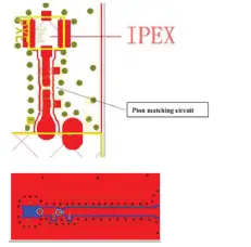
- When the OSM modules is used. a -matching circuit needs to be reserved between the WL_ANT antenna connector of the modules and the antenna connector of baseboard, and the recommended antenna matching circuit and initial parameters are shown in the following figure.
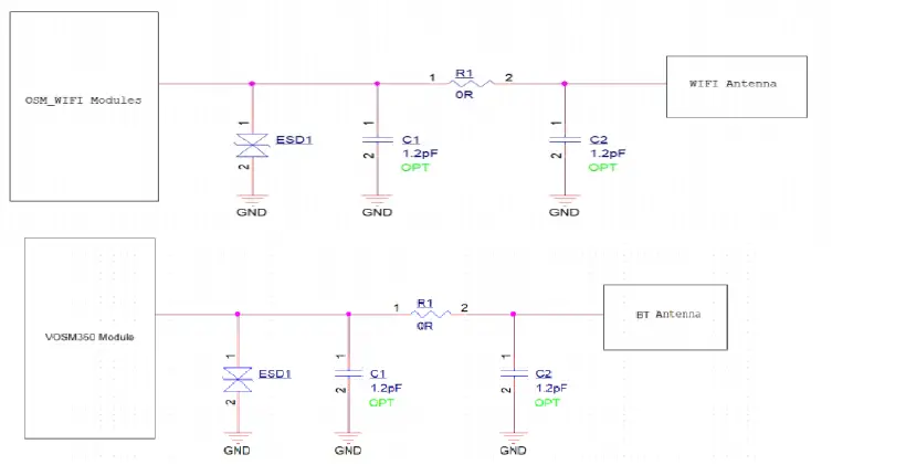 R1 default use 0 R resistor or 220pF capacitor, C1, C6 default, do match reserved. its final value according to the actual debugging results to determine.
The RF line layout should be matched according to 50oh m. The line impedance is related to the plate, plate thickness, line width and copper spacing. Professional software can be used to calculate the line width. Note: for multilayer plates, the plate thickness should calculate the distance from RF routing layer to GND of the next layer. There are RF lines Layout principles :
- RF line layout needs to match 50 ohms. The line width can be calculated by professional software. (Note: If it is a multi-layer board, The board thickness should calculate the distance from the RF trace layer to the next ground layer.)
- The RF line must be surrounded by ground copper and ground holes.
- The PI-type matching circuit for adjusting the impedance of the module is placed close to the module. The PI-type matching circuit for matching the antenna is placed close to the antenna.
RF exposure considerations:
The module must be installed in the host equipment such that at least 20cm is maintained between the antenna and users’ body. The device has been evaluated to meet general RF exposure requirement. Host product manufacturers need to provide a physical or e-label stating “Contains FCC ID: 2BEA6VOSM350” with their finished product. The device can be used in portable exposure condition without restriction.
Antenna:
Type: External Antenna@BT; External Antenna@WiFi
Impedance: 50 Ohm
- Manufacturer: DONGGUAN YIJIA ELECTRONICS COMMUNICATION TECHNOLOGY CO., LTD
- Model: YAA003R142
- Antenna Directivity(mainly describes the degree of radiation concentration of the antenna in a specific direction relative to the isotropic antenna.):
BT: 4.42dBi;
- WiFi ANT1: 4.42dBi@2.4GHz; 6.19dBi@5GHz
- WiFi ANT2: 4.42dBi@2.4GHz; 6.19dBi@5GHz
- Form Factor: External Antenna@BT; External Antenna@WiFi
- Bandwidth: 90MHz@BT; 100MHz@2.4GWiFi; 700MHz@5GWiFi;
- Polarization: Linear Polarization
Antenna Gain:
- BT ANT: maximum 1.82dBi;
- WiFi ANT1:maximum 1.82dBi@2.4GHz; 3.49dBi@5GHz antenna gain
- WiFi ANT2:maximum 1.82dBi@2.4GHz; 3.49dBi@5GHz antenna gain
- After certification, adding a different antenna type requires a C2/3 PC.
- Information on test modes and additional testing requirements:
- Host manufacturer must perform test of radiated & conducted emission and spurious emission, e.t.c according to the actual test modes for a stand-alone modular transmitter in a host, as well as for multiple simultaneously transmitting modules or other transmitters in a host product. Only when all the test results of test modes comply with FCC requirements, then the end product can be sold legally.
Additional testing, Part 15 Subpart B disclaimer:
- The host product manufacturer is responsible for compliance with any other FCC rules that apply to the host not covered by the modular transmitter grant of certification. The final host product still requires Part 15 Subpart B compliance testing
- with the modular transmitter installed.
Note EMI Considerations:
- D04 Module Integration Guide has been considered as “best practice” for RF design engineering testing and evaluation of non-linear interactions which can generate additional non-compliant limits due to module placement to host components or properties. For standalone mode, D04 Module Integration Guide was referenced, and simultaneous mode considered for the host product to confirm compliance.
How to make changes:
Only the Grantee is permitted to make permissive changes.
Frequently Asked Questions (FAQ):
- Q: What are the recommended operating conditions for the VOSM350 module?
A: The recommended operating voltage for the SOM is between 2.6V to 5.25V. Ensure that the eMMC VCC, eMMC VCCQ, and LPDDR4 voltages are within the specified ranges for stable operation. - Q: Can I use the VOSM350 module in industrial IoT devices?
A: Yes, the VOSM350 module is designed to cater to various application scenarios, including industrial IoT devices. Ensure proper environmental conditions and power supply for reliable operation.
Documents / Resources
 |
Vantron VOSM350 System on Module [pdf] Owner's Manual VOSM350, VOSM350 System on Module, System on Module, Module |


