![]() Clock Selective Watchdog Timer
Clock Selective Watchdog Timer
32-bit RISC Microcontroller
Reference Manual
Clock Selective Watchdog Timer
(SIWDT-A)
Revision 3.3
2024-10
Toshiba Electronic Devices & Storage Corporation
Preface
Related Document
Document name
Clock Control and Operation Mode
Exception
Power Supply and Reset Operation
Product Information
Conventions
- Numeric formats follow the rules as shown below:
Hexadecimal: 0xABC
Decimal: 123 or 0d123 – Only when it needs to be explicitly shown that they are decimal numbers.
Binary: 0b111 – It is possible to omit the “0b” when the number of bits can be distinctly understood from a sentence. - “_N” is added to the end of signal names to indicate low active signals.
- It is called “assert” that a signal moves to its active level, “deassert” to its inactive level.
- When two or more signal names are referred, they are described like as [m:n].
Example: S[3:0] shows four signal names S3, S2, S1 and S0 together. - The characters surrounded by [ ] defines the register.
Example: [ABCD] - “N” substitutes suffix number of two or more same kind of registers, fields, and bit names.
Example: [XYZ1], [XYZ2], [XYZ3] → [XYZn] - “x” substitutes suffix number or character of units and channels in the register list.
- In case of unit, “x” means A, B, and C, …
Example: [ADACR0], [ADBCR0], [ADCCR0] → [ADxCR0] - In case of channel, “x” means 0, 1, and 2, …
Example: [T32A0RUNA], [T32A1RUNA], [T32A2RUNA] → [T32AxRUNA] - The bit range of a register is written like as [m: n].
Example: Bit[3: 0] expresses the range of bit 3 to 0. - The configuration value of a register is expressed by either the hexadecimal number or the binary number.
Example: [ABCD]<EFG> = 0x01 (hexadecimal), [XYZn]<VW> = 1 (binary) - Word and byte represent the following bit length.
Byte: 8 bits
Half word: 16 bits
Word: 32 bits
Double word: 64 bits - Properties of each bit in a register are expressed as follows:
R: Read only
W: Write only
R/W: Read and write are possible. - Unless otherwise specified, register access supports only word access.
- The register defined as “Reserved” must not be rewritten. Moreover, do not use the read value.
- The value read from the bit having default value of “-” is unknown.
- When a register containing both of writable bits and read-only bits is written, read-only bits should be written with their default value, In the cases that default is “-“, follow the definition of each register.
- Reserved bits of the write-only register should be written with their default value. In the cases that default is “-“, follow the definition of each register.
- Do not use read-modified-write processing to the register of a definition which is different by writing and read out.
All other company names, product names, and service names mentioned herein may be trademarks of their respective companies.
Terms and Abbreviations
Some of abbreviations used in this document are as follows:
| SIWDT | Clock Selective Watchdog Timer |
Outlines
When the CPU executes mal function (a runaway) caused by a noise or others, the watchdog timer detects it and gives a trigger to the CPU to resume the correct function.
| Function classification | Function | Operation |
| Timer control | Clock selection | It is possible to select the source clock of runaway detection from “fsys/4”, “fIHOSC1″,”fIHOSC2”. |
| Detection time control | It is possible to select the detection time between 215 to 229 count of the selection clock. | |
| Decision control | Window selection | It is possible to select the clear window of runaway detection from “No settings”, “Later 1/2” and “Last 1/4”. |
| Detection control | Detection behavior | It is possible to select behavior of the runaway detection from “Interrupt” and “Reset”. |
| Protection control | Mode selection | It is possible to select the “Protection A mode” which cannot be released except for RESET, and “Protection B mode” which can be released by /SIWDxPRO]<PROTECT[7:01>. |
| Control of modification of the oscillation clock control bit of the internal high-speed oscillator 2 (IHOSC2) | It is possible to control modification of the oscillation clock control bit of the internal high-speed oscillator 2 (IHOSC2). |
Configuration
Figure 2.1 shows the block diagram of the watchdog timer.
 Figure 2.1 SIWDT Block Diagram
Table 2.1 List of Signals
| No. | Symbol | Signal name | 110 | Related reference manual |
| 1 | fsys | System clock | Input | Clock Control and Operation Mode |
| 2 | f IHOSC1 | Internal oscillator 1 | Input | Clock Control and Operation Mode |
| 3 | f IHOSC2 | Internal oscillator 2 | Input | Clock Control and Operation Mode |
| 4 | INTWDTx | Watchdog timer interrupt | Output | Exception |
| 5 | WDTRSTOUT | Watchdog timer reset | Output | Power Supply and Reset Operation Clock Control and Operation Mode (Note) |
| 6 | OSCPRO | Control of modification of the oscillation clock control bit of the internal high-speed _ oscillator 2 (IHOSC2) | Output | Product Information |
Note: Refer to “Power Supply and Reset Operation” for TXZ family and “Clock Control and Operation Mode” for TX family and TXZ+ family.
Function and Operation
3.1. Basic Operation
The watchdog timer (WDT) is for detecting malfunctions (runaway) of the CPU caused by noises or other disturbances and remedying them to return the CPU to normal operation.
If the watchdog timer detects a runaway, it generates an INTWDTx interrupt or reset. When the clear code (0x4E) is written to the [SIWDxCR] register, the counter is cleared and re-starts the count.
3.2. Clock Supply
The SIWDT starts the count immediately after the reset is deasserted. The selected clock is “the system clock (fsys) of 4 division” at that time. If the watchdog timer is not used, it should be disabled. When the setting is changed, it should be disabled, too.
3.3. Clock Selection Circuit
3.3.1. Clock Selection
The clock which is selected from “the system clock (fsys) of 4 division”, “internal oscillation clock “1” (fIHOSC1)”, and “internal oscillation clock 2 (fIHOSC2)” by [SIWDxMOD] <WDLCS[1:0]>, is used as input clock.
3.3.2. Clock Run and Stop
When a counter clock to SIWDT is stopped, the SIWDT must be stopped.
The operation of SIWDT set to “1” to [SIWDxEN]<WDTE>.
The [SIWDxCR] register should be set to disable code (0xB1) after the [SIWDxEN]<WDTE> set to “0” for stopping SIWDT. The SIWDT is disabled, and counter is cleared.
3.4. Detection Time Control
The detection time is selected from among 2¹⁵, 2¹⁷, 2¹⁹, 2²¹, 2²³, 2²⁵, 2²⁷ and 2²⁹ by [SIWDxMOD]<WDTP [2:0]>.
3.5. Detection Operation Control
The generator which is selected by the [SIWDxMOD]<RESCR> after the elapse of detection time, is “watchdog timer interrupt (INTWDTx)”, or “reset”.
3.6. Window Control
3.6.1. Clear Window Setting
The clear window is selected with [SIWDxMOD] <WDCWD[1:0]> from among none specified, the latter half of the detection interval, and the last quarter of the detection interval.
If the clear code is written during the clear window interval, the counter is cleared and re-starts the count.
 Figure 3.1 Clear Code Writes during Clear Window Interval
If the clear code is written before the clear window, the operation is as follows according to the setting of [SIWDxMOD]<RESCR>.
When [SIWDxMOD]<RESCR> = 1 and the reset generation is enabled, the reset is asserted and the SIWDT becomes the initialization state.
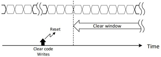 Figure 3.2 Clear Code Writes before Clear Window (1)
When [SIWDxMOD]<RESCR> = 0 or the INTWDTx generation is enabled, the INTWDTx is generated and [SIWDxMOD]<INTF> is set to “1” every write of the clear code. The counter continues the count and the INTWDTx is generated at the detection time, again.
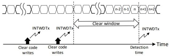 Figure 3.3 Clear Code Writes before Clear Window (2)
3.7. Protection Control
3.7.1. Protection Mode
There are two types of protection modes to prevent from unexpected writing. Its setting should be done while [SIWDxEN]<WDTE> is “1”.
(a) Protection A mode
[SIWDxPRO] <PROTECT[7:0]> should be set to 0xA9 to select the protection A mode.
Only 0x4E (Clear code) can be written to [SIWDxCR] <WDCR[7:0]> in this mode. Other code write is ignored.
The protection A mode can be cleared only by the reset initialization.
(b) Protection B mode
[SIWDxPRO]< PROTECT[7:0]>should be set to 0x74 to select the protection B mode.
Only 0x4E (Clear code) can be written to [SIWDxCR] <WDCR[7:0]> and only 0x1E (protection B mode clear) can be written to [SIWDxPRO] <PROTECT[7:0]>. Other code write to the fields is ignored.
3.7.2. Oscillation Control of Internal High-speed Oscillator 2 (IHOSC2)
When [SIWDxOSCCR]<OSCPRO> is set to “1”, the write is inhibited to the oscillation clock control bit of the internal high-speed oscillator 2 (IHOSC2).
For the internal oscillation clock control bit, refer to reference manual “Product Information”.
3.8. Count Monitor
The [SIWDxMONI]<MONI[29:0]> should be read multiple times. When the read value is different. it is shown that the counter is working.
3.9. Operation Status of Counter
In debug halt, the counter of SIWDT is stopped.
Refer to reference manual “Clock Control and Operation Mode” for each operation mode.
Registers
4.1. List of Registers
The control registers and their addresses are shown as follows:
| Peripheral function | Channel /Unit | Base address | |||
| TYPE1 | TYPE2 | TYPE3 | |||
| Watchdog Timer | SIWDT | ch0 | 0x400BB400 | 0x400A0600 | 0x40040600 |
| ch1 | – | 0x400A0700 | 0x40040700 | ||
Note: The channel/unit and base address type are different by products. Please refer to “Products Information” of the reference manual for the details.
| Register name | Address (Base+) | |
| Protection Register | [SIWDxPRO] | 0x0000 |
| Enable Register | [SIWDxEN] | 0x0004 |
| Control Register | [SIWDxCR] | 0x0008 |
| Mode Register | [SIWDxMOD] | 0x000C |
| Count Monitor Register | [SIWDxMONI] | 0x0010 |
| Oscillation Clock Protect Control Register | [SIWDxOSCCR] | 0x0014 |
4.2. Details of Registers
4.2.1. [SIWDxPRO] (Protection Register)
| Bit | Bit symbol | After reset | Type | Function |
| 31:8 | – | 0 | R | Read as “0”. |
| 7:0 | PROTECT[7:0] | 0x1E | R/W | Protection mode 0x1E: No protection 0xA9: Protection A mode setting 0x74: Protection B mode setting The other settings are ignored. |
Note: When [SIWDxEN]<WDTF> is “Operating”, this field can be written except in the protection A mode.
4.2.2. [SIWDxEN] (Enable Register)
| Bit | Bit symbol | After reset | Type | Function |
| 31:2 | – | 0 | R | Read as “0”. |
| 1 | WDTF | 1 | R | Operation flag 0: Stop 1: Operating SIWDT operation status is shown. |
| 0 | WDTE | 1 | R/W | Enable or disable control 0: Disabled 1: Enabled When the watchdog timer is disabled, it is necessary to disable that this bit should be set to 0 and then the disable code (0xB1) should be written to [SIWDxCR]<WDCR[7:0]>. [SIWDxEN]<WDTE> should be set to 1 to return to the enable state. |
4.2.3. [SIWDxCR] (Control Register)
| Bit | Bit symbol | After reset | Type | Function |
| 31:8 | – | 0 | R | Read as “0”. |
| 7:0 | WDCR[7:0] | Undefined | W | Disable code and clear code 0xB1: Disable code 0x4E: Clear code The other codes writing is ignored. |
4.2.4. [SIWDxMOD] (Mode Register)
| Bit | Bit symbol | After reset | Type | Function |
| 31:14 | – | 0 | R | Read as “0”. |
| 13:12 | WDCLS[1:0] | 00 | R/W | Clock selection 00: fsys/4 01: Internal oscillation clock 1 (fIHOSC1) 10: Internal oscillation clock 2 (fIHOSC2) 11: Reserved |
| 11 | – | 0 | R | Read as “0”. |
| 10:8 | WDTP[2:0] | 000 | R/W | Detection time selection (fIWD = The clock which is selected by <WDCLS>) 000: 215/fIWD 001: 217/fIWD 010: 219/fIWD 011: 221/fIWD 100: 223/fIWD 101: 225/fIWD 110: 227/fIWD 111: 229/fIWD |
| 7:6 | – | 0 | R | Read as”0″. |
| 5:4 | WDCWD[1:0] | 00 | R/W | Clear window setting 00: No setting 01: Second half 10: Last quarter 11: Reserved |
| 3:2 | – | 0 | R | Read as “0”. |
| 1 | INTF | 0 | R | INTWDTx generation by the clear code write before the clear window 0: Not generated 1: Generated |
| W | The clear set of flag 0: don’t care 1: clear to “0”. |
|||
| 0 | RESCR | 1 | R/W | Operation after the runaway detection 0: INTWDTx interrupt request is generated. 1: Reset is generated. |
Note: This can be written when [SIWDxEN]<WDTF> is “Stop” except in the protection setting state.
4.2.5. [SIWDxMONI] (Count Monitor Register)
| Bit | Bit symbol | After reset | Type | Function |
| 31:30 | – | 0 | R | Read as “0”. |
| 29:0 | MONI[29:0] | Undefined | R | Counter monitor This register should be read multiple times. When the read values are different, it is shown that the counter is working. The read value is not precisely correct. It should be used as a reference value. |
4.2.6. [SIWDxOSCCR] (Oscillation Clock Protect Control Register)
| Bit | Bit symbol | After reset | Type | Function |
| 31:1 | – | 0 | R | Read as”0″… |
| 0 | OSCPRO | 0 | R/W | Write protection for the oscillation clock control bit of the internal high- speed oscillator 2 (IHOSC2). (Note2) 0: Disabled 1: Enabled |
Note 1: When [SIWDxEN]<WDTF> is “Stop”, this bit can be written except in the protection setting state.
Note 2: For the oscillation clock control bit of the internal high-speed oscillator 2 (IHOSC2), refer to reference manual “Product Information”.
Precaution
- When [SIWDxPRO] <PROTECT[7:0]> is “0x1E” (No protection) or “0x74” (Protection B mode) Before CPU transfers low-power consumption mode (STOP1/STOP2/IDLE) from NORMAL mode, the watchdog timer should be disabled. For details of setting procedure, refer to the reference manual “Clock Control and Operation Mode”.
- When [SIWDxPRO] <PROTECT[7:0]> is ” 0x9A” (Protection A mode)
The count clock operation in each low-power consumption mode is shown in Table 5.1. For the oscillation clock control bit of the internal high-speed oscillator 2 (IHOSC2), refer to the reference manual “Product Information”.
Table 5.1 Count Clock Operation in Each Low-power Consumption Mode
| Count clock | IDLE mode | STOP1 mode | |
| fsys/4 | Keep up | Stopped | |
| fIHOSC1 | Keep up | Stopped | |
| fIHOSC2 | When oscillation clock control bit is [CGOSCCR]<IHOSC2EN> |
Keep up | Stopped |
| When oscillation clock control bit is [RLMLOSCCR]<POSCEN> | Keep up | Keep up | |
Revision History
Table 6.1 Revision History
| Revision | Date | Description |
| 1.0 | 2017-09-08 | First release |
| 2.0 | 2018-03-23 | – 3.5 Detection Behavior Control Added INTWDTx in “watchdog timer interrupt” – 3.9 Operation Mode and Operation Status Added Table 3.1 – 4.1 List of Register Modified Note – 4.2.4 [SIWDxMOD] Modified INTWDT to INTWDTx of <INTF><RESCR> – Precaution Modified explanation |
| 3.0 | 2018-06-19 | – 1 Outlines Deleted Table title – 4.1 List of Registers Added base address of TYPE2(ch1) and TYPE3 – 4.2.3 [SIWDxCR] Modified after reset value of <WDCR[7:0]> to undefined – 4.2.5 [SIWDxMONI] Modified after reset value of <MONI[29:0]> to undefined |
| 3.1 | 2023-06-14 | – 1. Outlines Name and description of the 2nd function of “Protection Control” are changed. – Table 2.1 List of Signals Signal name and related reference manual of OSCPRO are changed. – 3.2. Clock Supply The description is changed. – 3.7.2. Oscillation Clock Control Bit of Internal High-speed Oscillator 2 (IHOSC2) The description for the oscillation clock control bit of the internal high-speed Oscillator 2 (IHOSC2) is changed. – 3.9. Operation Status of Counter A table is deleted. The description for the counter is changed. – 4.2.6. [SIWDxOSCCR] (Oscillation Enable Register) The description for <OSCPRO> is changed. Note 2 is changed. – 5. Precaution The description is changed. |
| 3.2 | 2023-09-15 | – Table 2.1 List of Signals Corrected reference manual name for WDTRSTOUT. |
| 3.3 | 2024-10-31 | – Appearance updated |
RESTRICTIONS ON PRODUCT USE
Toshiba Corporation and its subsidiaries and affiliates are collectively referred to as “TOSHIBA”.
Hardware, software and systems described in this document are collectively referred to as “Product”.
- TOSHIBA reserves the right to make changes to the information in this document and related Product without notice.
- This document and any information herein may not be reproduced without prior written permission from TOSHIBA. Even with TOSHIBA’s written permission, reproduction is permissible only if reproduction is without alteration/omission.
- Though TOSHIBA works continually to improve Product’s quality and reliability, Product can malfunction or fail. Customers are responsible for complying with safety standards and for providing adequate designs and safeguards for their hardware, software and systems which minimize risk and avoid situations in which a malfunction or failure of Product could cause loss of human life, bodily injury or damage to property, including data loss or corruption. Before customers use the Product, create designs including the Product, or incorporate the Product into their own applications, customers must also refer to and comply with (a) the latest versions of all relevant TOSHIBA information, including without limitation, this document, the specifications, the data sheets and application notes for Product and the precautions and conditions set forth in the “TOSHIBA Semiconductor Reliability Handbook” and (b) the instructions for the application with which the Product will be used with or for. Customers are solely responsible for all aspects of their own product design or applications, including but not limited to (a) determining the appropriateness of the use of this Product in such design or applications; (b) evaluating and determining the applicability of any information contained in this document, or in charts, diagrams, programs, algorithms, sample application circuits, or any other referenced documents; and (c) validating all operating parameters for such designs and applications. TOSHIBA ASSUMES NO LIABILITY FOR CUSTOMERS’ PRODUCT DESIGN OR APPLICATIONS.
- PRODUCT IS NEITHER INTENDED NOR WARRANTED FOR USE IN EQUIPMENTS OR SYSTEMS THAT REQUIRE EXTRAORDINARILY HIGH LEVELS OF QUALITY AND/OR RELIABILITY, AND/OR A MALFUNCTION OR FAILURE OF WHICH MAY CAUSE LOSS OF HUMAN LIFE, BODILY INJURY, SERIOUS PROPERTY DAMAGE AND/OR SERIOUS PUBLIC IMPACT (“UNINTENDED USE”). Except for specific applications as expressly stated in this document, Unintended Use includes, without limitation, equipment used in nuclear facilities, equipment used in the aerospace industry, medical equipment, equipment used for automobiles, trains, ships and other transportation, traffic signaling equipment, equipment used to control combustions or explosions, safety devices, elevators and escalators, devices related to electric power, and equipment used in finance-related fields. IF YOU USE PRODUCT FOR UNINTENDED USE, TOSHIBA ASSUMES NO LIABILITY FOR PRODUCT. For details, please contact your TOSHIBA sales representative.
- Do not disassemble, analyze, reverse-engineer, alter, modify, translate or copy Product, whether in whole or in part.
- Product shall not be used for or incorporated into any products or systems whose manufacture, use, or sale is prohibited under any applicable laws or regulations.
- The information contained herein is presented only as guidance for Product use. No responsibility is assumed by TOSHIBA for any infringement of patents or any other intellectual property rights of third parties that may result from the use of Product. No license to any intellectual property right is granted by this document, whether express or implied, by estoppel or otherwise.
- ABSENT A WRITTEN SIGNED AGREEMENT, EXCEPT AS PROVIDED IN THE RELEVANT TERMS AND CONDITIONS OF SALE FOR PRODUCT, AND TO THE MAXIMUM EXTENT ALLOWABLE BY LAW, TOSHIBA (1) ASSUMES NO LIABILITY WHATSOEVER, INCLUDING WITHOUT LIMITATION, INDIRECT, CONSEQUENTIAL, SPECIAL, OR INCIDENTAL DAMAGES OR LOSS, INCLUDING WITHOUT LIMITATION, LOSS OF PROFITS, LOSS OF OPPORTUNITIES, BUSINESS INTERRUPTION AND LOSS OF DATA, AND (2) DISCLAIMS ANY AND ALL EXPRESS OR IMPLIED WARRANTIES AND CONDITIONS RELATED TO SALE, USE OF PRODUCT, OR INFORMATION, INCLUDING WARRANTIES OR CONDITIONS OF MERCHANTABILITY, FITNESS FOR A PARTICULAR PURPOSE, ACCURACY OF INFORMATION, OR NONINFRINGEMENT.
- Do not use or otherwise make available Product or related software or technology for any military purposes, including without limitation, for the design, development, use, stockpiling or manufacturing of nuclear, chemical, or biological weapons or missile technology products (mass destruction weapons). Product and related software and technology may be controlled under the applicable export laws and regulations including, without limitation, the Japanese Foreign Exchange and Foreign Trade Law and the U.S. Export Administration Regulations. Export and re-export of Product or related software or technology are strictly prohibited except in compliance with all applicable export laws and regulations.
- Please contact your TOSHIBA sales representative for details as to environmental matters such as the RoHS compatibility of Product. Please use Product in compliance with all applicable laws and regulations that regulate the inclusion or use of controlled substances, including without limitation, the EU RoHS Directive. TOSHIBA ASSUMES NO LIABILITY FOR DAMAGES OR LOSSES OCCURRING AS A RESULT OF NONCOMPLIANCE WITH APPLICABLE LAWS AND REGULATIONS.
Toshiba Electronic Devices & Storage Corporation
https://toshiba.semicon-storage.com/
Documents / Resources
 |
TOSHIBA SIWDT-A Clock Selective Watchdog Timer [pdf] Instruction Manual SIWDT-A Clock Selective Watchdog Timer, SIWDT-A, Clock Selective Watchdog Timer, Selective Watchdog Timer, Watchdog Timer, Timer |