TEXAS INSTRUMENTS WL1837MOD WLAN MIMO and Bluetooth Module
The WL1837MOD is a Wi-Fi® dual-band, Bluetooth, and BLE module. The WL1837MOD is a certified WiLink™ 8 module that offers high throughput and extended range along with Wi-Fi and Bluetooth coexistence in a power-optimized design. The WL1837MOD offers A 2.4- and 5-GHz module solution with two antennas supporting industrial temperature grade. The module is FCC and IC certified for AP (with DFS support) and client.
Key Benefits
The WL1837MOD offers the following benefits:
- Reduces design overhead: Single WiLink 8 module scales across Wi-Fi and Bluetooth
- WLAN high throughput: 80 Mbps (TCP), 100 Mbps (UDP)
- Bluetooth 4.1 + BLE (Smart Ready)
- Wi-Fi and Bluetooth single-antenna coexistence
- Low power at 30% to 50% less than the previous generation
- Available as an easy-to-use FCC-certified module
- Lower manufacturing costs saves board space and minimizes RF expertise.
- AM335x Linux and Android reference platform accelerates customer development and time to market.
Antenna Characteristics
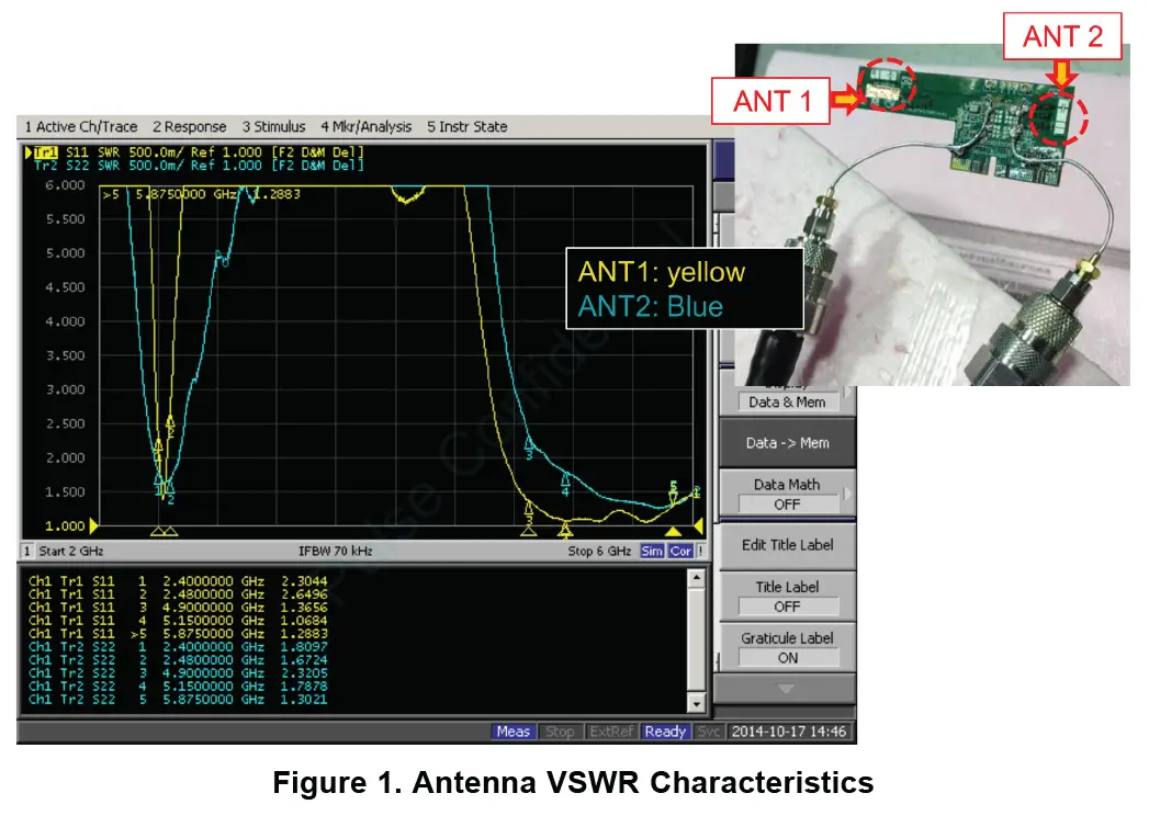
VSWR
Figure 1 shows the antenna VSWR characteristics.
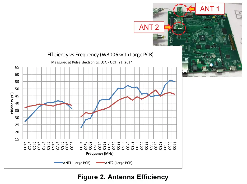
Efficiency
Figure 2 shows the antenna efficiency.
Radio Pattern
For information on the antenna radio pattern and other related information, see productfinder.pulseeng.com/product/W3006
Layout Guidelines
Board Layout
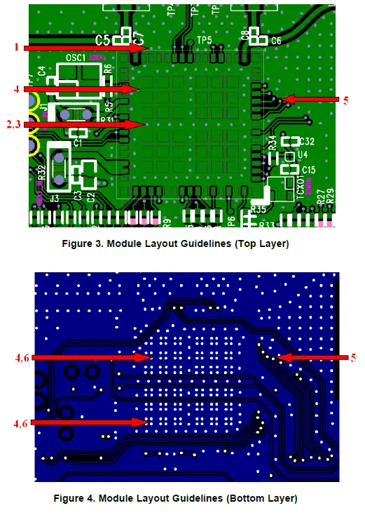
Table 1 describes the guidelines corresponding to the reference numbers in Figure 3 and Figure 4.
Table 1. Module Layout Guidelines
| Reference | Guideline Description |
| 1 | Keep the proximity of ground vias close to the pad. |
| 2 | Do not run signal traces underneath the module on the layer where the module is mounted. |
| 3 | Have a complete ground pour in layer 2 for thermal dissipation. |
| 4 | Ensure a solid ground plane and ground vias under the module for stable system and thermal dissipation. |
| 5 | Increase ground pour in the first layer and have all traces from the first layer on the inner layers, if possible. |
| 6 | Signal traces can be run on a third layer under the solid ground layer and the module mounting layer. |
Figure 5 shows the trace design for the PCB. Orcawest Holdings, LLC dba E.I. Medical Imaging recommends using a 50-Ω impedance match on the trace to the antenna and 50-Ω traces for the PCB layout.
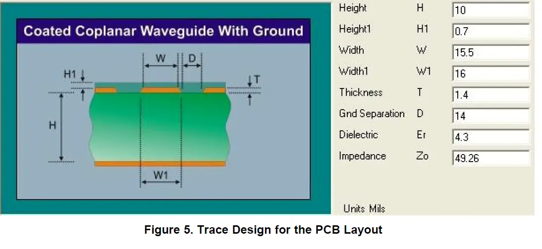
Figure 6 and Figure 7 show instances of good layout practices for the antenna and RF trace routing.
NOTE: RF traces must be as short as possible. The antenna, RF traces, and modules must be on the edge of the PCB product. The proximity of the antenna to the enclosure and the enclosure material must also be considered.
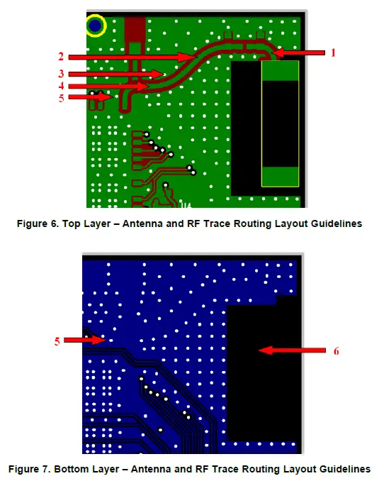
Table 2. Antenna and RF Trace Routing Layout Guidelines
| Reference | Guideline Description |
| 1 | The RF trace antenna feed must be as short as possible beyond the ground reference. At this point, the trace starts to radiate. |
| 2 | RF trace bends must be gradual with an approximate maximum bend of 45 degrees with trace mitered. RF traces must not have sharp corners. |
| 3 | RF traces must have via stitching on the ground plane beside the RF trace on both sides. |
| 4 | RF traces must have constant impedance (microstrip transmission line). |
| 5 | For best results, the RF trace ground layer must be the ground layer immediately below the RF trace. The ground layer must be solid. |
| 6 | There must be no traces or ground under the antenna section. |
Figure 8 shows the MIMO antenna spacing. The distance between ANT1 and ANT2 must be greater than half the wavelength (62.5 mm at 2.4 GHz).

Follow these supply routing guidelines:
- For power supply routing, the power trace for VBAT must be at least 40-mil wide.
- The 1.8-V trace must be at least 18-mil wide.
- Make VBAT traces as wide as possible to ensure reduced inductance and trace resistance.
- If possible, shield VBAT traces with ground above, below, and beside the traces.
Follow these digital-signal routing guidelines:
- Route SDIO signal traces (CLK, CMD, D0, D1, D2, and D3) in parallel to each other and as short as possible (less than 12 cm). In addition, each trace must be the same length. Ensure enough space between traces (greater than 1.5 times the trace width or ground) to ensure signal quality, especially for the SDIO_CLK trace. Remember to keep these traces away from the other digital or analog signal traces. TI recommends adding ground shielding around these buses.
- Digital clock signals (SDIO clock, PCM clock, and so on) are a source of noise. Keep the traces of these signals as short as possible. Whenever possible, maintain a clearance around these signals.
Manual Information to the End User
The OEM integrator has to be aware not to provide information to the end user regarding how to install or remove this RF module in the user’s manual of the end product which integrates this module. The end user manual shall include all required regulatory information/warnings as show in this manual.
Federal Communication Commission Interference Statement
This device complies with Part 15 of the FCC Rules. Operation is subject to the following two conditions: (1) This device may not cause harmful interference, and (2) this device must accept any interference received, including interference that may cause undesired operation.
This equipment has been tested and found to comply with the limits for a Class B digital device, pursuant to Part 15 of the FCC Rules. These limits are designed to provide reasonable protection against harmful interference in a residential installation. This equipment generates, uses and can radiate radio frequency energy and, if not installed and used in accordance with the instructions, may cause harmful interference to radio communications. However, there is no guarantee that interference will not occur in a particular installation. If this equipment does cause harmful interference to radio or television reception, which can be determined by turning the equipment off and on, the user is encouraged to try to correct the interference by one of the following measures:
- Reorient or relocate the receiving antenna.
- Increase the separation between the equipment and receiver.
- Connect the equipment into an outlet on a circuit different from that to which the receiver is connected.
- Consult the dealer or an experienced radio/TV technician for help.
Any changes or modifications not expressly approved by the party responsible for compliance could void the user’s authority to operate this equipment.
This transmitter must not be co-located or operating in conjunction with any other antenna or transmitter.
Industry Canada Statement
This device complies with Industry Canada license-exempt RSS standard(s). Operation is subject to the following two conditions:
- This device may not cause interference, and
- This device must accept any interference, including interference that may cause undesired operation of the device.
CAN ICES-3(B)/ NMB-3(B)
The device could automatically discontinue transmission in case of absence of information to transmit, or operational failure. Note that this is not intended to prohibit transmission of control or signaling information or the use of repetitive codes where required by the technology.
- The device for operation in the band 5150–5250 MHz is only for indoor use to reduce the potential for harmful interference to co-channel mobile satellite systems;
- The maximum antenna gain permitted for devices in the bands 5250–5350 MHz and 5470–5725 MHz shall comply with the e.i.r.p. limit; and
- The maximum antenna gain permitted for devices in the band 5725–5825 MHz shall comply with the e.i.r.p. limits specified for point-to-point and non point-to-point operation as appropriate.
In addition, high-power radars are allocated as primary users (i.e. priority users) of the bands 5250–5350 MHz and 5650–5850 MHz and that these radars could cause interference and/or damage to LE-LAN devices.
Radiation Exposure Statement
This equipment complies with FCC/IC radiation exposure limits set forth for an uncontrolled environment. This equipment should be installed and operated with minimum distance 20 cm between the radiator & your body.
End Product Labeling
When the module is installed in the host device, the FCC/IC ID label must be visible through a window on the final device or it must be visible when an access panel, door or cover is easily
removed. If not, a second label must be placed on the outside of the final device that contains the following text:
“Contains FCC ID: XMO-WL18DBMOD”
“Contains IC: 8512A-WL18DBMOD “
The grantee’s FCC ID/IC ID can be used only when all FCC/IC compliance requirements are met.
This device is intended only for OEM integrators under the following conditions:
- The antenna must be installed such that 20 cm is maintained between the antenna and users.
- The transmitter module may not be co-located with any other transmitter or antenna.
- This radio transmitter may only operate using an antenna of a type and maximum (or lesser) gain approved by Texas Instrument. Antenna types not included in the list, having a gain greater than the maximum gain indicated for that type, are strictly prohibited for use with this transmitter.
| Antenna Gain (dBi) @ 2.4GHz | Antenna Gain (dBi) @ 5GHz |
| 3.2 | 4.5 |
In the event that these conditions cannot be met (for example certain laptop configurations or co-location with another transmitter), then the FCC/IC authorization is no longer considered valid and the FCC ID/IC ID cannot be used on the final product. In these circumstances, the OEM integrator will be responsible for re-evaluating the end product (including the transmitter) and obtaining a separate FCC/IC authorization.
Documents / Resources
 |
TEXAS INSTRUMENTS WL1837MOD WLAN MIMO and Bluetooth Module [pdf] User Guide XMO-WL18DBMOD, XMOWL18DBMOD, wl18dbmod, WL1837MOD WLAN MIMO and Bluetooth Module, WL1837MOD, WLAN MIMO and Bluetooth Module, MIMO and Bluetooth Module, Bluetooth Module, Module |