LCD WIKI E32R32P, E32N32P 3.2inch IPS ESP32-32E
Display Module User Manual

Resource Description
The resource directory is shown in the following figure:
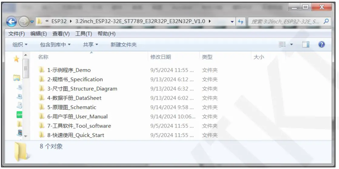
Figure 1.1 Product Information Pack catalog

Software Instructions
Display module software development steps are as follows:
A. Build ESP32 platform software development environment;
B. if necessary, import third-party software libraries as a basis for development;
C. open the software project to be debugged, you can also create a new software project;
D. power on the display module, compile and download the debugging program, and then check the software running effect;
E. the software effect does not reach the expected, continue to modify the program code, and then compile and download, until the effect reaches the expected;
For details about the preceding steps, see the documentation in the 1-Demo directory.
Hardware Instructions
3.1. Overview of module hardware resources is displayed
Module hardware resources are shown in the following two figures:
Module hardware resources are shown in the following two figures:

Figure 3.1 Module hardware resources 1

Figure 3.2 Module hardware resources 2
The hardware resources are described as follows:
1) LCD
The LCD display size is 3.2 inches, the driver IC is ST7789, and the resolution is 240×320. The ESP32 is connected using a 4-wire SPI communication interface.
A. Introduction to ST7789 controller
The ST7789 controller supports a maximum resolution of 240*320 and a 172800-byte GRAM. It also supports 8-bit, 9-bit, 16-bit, and 18-bit parallel port data buses. It also supports 3-wire and 4-wire SPI serial ports. Since parallel control requires a large number of IO ports, the most common one is SPI serial port control. The ST7789 also supports 65K, 262K RGB color display, display color is very rich, while supporting rotating display and scroll display and video playback, display in a variety of ways.
The ST7789 controller uses 16bit (RGB565) to control a pixel display, so it can display up to 65K colors per pixel. The pixel address setting is performed in the order of rows and columns, and the incrementing and decreasing direction is determined by the scanning mode. The ST7789 display method is performed by setting the address and then setting the color value.
B. Introduction to SPI communication protocol
The writing mode timing of the 4-wire SPI bus is shown in the following figure:

Figure 3.3 Writing mode timing of 4-wire SPI bus
CSX is a slave chip selection, and the chip will only be enabled when CSX is at low power level.
D/CX is the data/command control pin of the chip. When DCX is writing commands at low levels, data is written at high levels
SCL is the SPI bus clock, with each rising edge transmitting 1 bit of data;
SDA is the data transmitted by SPI, which transmits 8 bits of data at once. The data format is shown in the following figure:

Figure 3.4 4 SPI transmission data format
High bit first, transmit first.
For SPI communication, data has a transmission timing, with a combination of real-time clock phase (CPHA) and clock polarity (CPOL):
The level of CPOL determines the idle state level of the serial synchronous clock, with CPOL=0, indicating a low level. CPOL pair transmission protocol
The discussion did not have much influence;
The height of CPHA determines whether the serial synchronous clock collects data on the first or second clock jump edge,
When CPHL=0, perform data collection at the first transition edge;
The combination of these two forms four SPI communication methods, and SPI0 is commonly used in China, where CPHL=0 and CPOL=0
When CPHL=0, perform data collection at the first transition edge;
The combination of these two forms four SPI communication methods, and SPI0 is commonly used in China, where CPHL=0 and CPOL=0
2) Resistive Touch Screen
The resistive touch screen is 3.2 inches in size and is connected to the XPT2046 control IC through four pins: XL, XR, YU, YD.
The resistive touch screen is 3.2 inches in size and is connected to the XPT2046 control IC through four pins: XL, XR, YU, YD.
3) ESP32-WROOM-32E Module
This module has a built-in ESP32-DOWD-V3 chip, Xtensa dual-core 32-bit LX6 microprocessor, and supports clock rates up to 240MHz. It has 448KB ROM, 520KB SRAM, 16KB RTC SRAM, and 4MB QSPI Flash. 2.4GHz WIFI, Bluetooth V4.2 and Bluetooth Low power modules are supported. External 26 GPIOs, support SD card,
UART, SPI, SDIO, I2C, LED PWM, motor PWM, I2S, IR, pulse counter, GPIO, capacitive touch sensor, ADC, DAC, TWAI and other peripherals.
4) MicroSD Card Slot
Using SPI communication mode and ESP32 connection, support for MicroSD cards of various capacities.
Using SPI communication mode and ESP32 connection, support for MicroSD cards of various capacities.
5) RGB Three-Color LED
Red, green and blue LED lights can be used to indicate the running status of the program.
Red, green and blue LED lights can be used to indicate the running status of the program.
6) Serial Port
An external serial port module is used for serial port communication.
An external serial port module is used for serial port communication.
7) USB to Serial Port and One-Click Download Circuit
The core device is CH340C, one end is connected to the computer USB, one end is connected to the ESP32 serial port, so as to achieve USB to TTL serial port.
In addition, a one-click download circuit is also attached, that is, when downloading the program, it can automatically enter the download mode, without the need to touch through the external.
8) Battery Interface
Two-pin interface, one for the positive electrode, one for the negative electrode, access the battery power supply and charging.
Two-pin interface, one for the positive electrode, one for the negative electrode, access the battery power supply and charging.
9) Battery Charge and Discharge Management Circuit
The core device is TP4054, this circuit can control the battery charging current, the battery is safely charged to saturation state, but also can safely control the battery discharge.
The core device is TP4054, this circuit can control the battery charging current, the battery is safely charged to saturation state, but also can safely control the battery discharge.
10) BOOT Key
After the display module is powered on, pressing will lower IO0. If the moment the module is powered on or the ESP32 is reset, lowering IO0 will enter the download mode. Other cases can be used as ordinary buttons.
After the display module is powered on, pressing will lower IO0. If the moment the module is powered on or the ESP32 is reset, lowering IO0 will enter the download mode. Other cases can be used as ordinary buttons.
11) Type-C Interface
The main power supply interface and program download interface of the display module. Connect USB to serial port and one-click download circuit, can be used for power supply, download and serial communication.
The main power supply interface and program download interface of the display module. Connect USB to serial port and one-click download circuit, can be used for power supply, download and serial communication.
12) 5V to 3.3V Voltage Regulator Circuit
The core device is the ME6217C33M5G LDO regulator. The voltage regulator circuit supports 2V~6.5V wide voltage input, 3.3V stable voltage output, and the maximum output current is 800mA, which can fully meet the voltage and current requirements of the display module.
The core device is the ME6217C33M5G LDO regulator. The voltage regulator circuit supports 2V~6.5V wide voltage input, 3.3V stable voltage output, and the maximum output current is 800mA, which can fully meet the voltage and current requirements of the display module.
13) RESET Key
After the display module is powered on, pressing will pull the ESP32 reset pin down (the default state is pull up), so as to achieve the reset function.
After the display module is powered on, pressing will pull the ESP32 reset pin down (the default state is pull up), so as to achieve the reset function.
14) Resistive Touch Screen Control Circuit
The core device is XPT2046, which communicates with the ESP32 through SPI.
This circuit is the bridge between the resistive touch screen and the ESP32 master, responsible for transmitting the data on the touch screen to the ESP32 master, so as to obtain the coordinates of the touch point.
The core device is XPT2046, which communicates with the ESP32 through SPI.
This circuit is the bridge between the resistive touch screen and the ESP32 master, responsible for transmitting the data on the touch screen to the ESP32 master, so as to obtain the coordinates of the touch point.
15) Expand the Input Pin
The two unused input IO ports on the ESP32 module are drawn out for peripheral use.
The two unused input IO ports on the ESP32 module are drawn out for peripheral use.
16) Backlight Control Circuit
The core device is BSS138 field effect tube. One end of this circuit is connected to the backlight control pin on the ESP32 master, and the other end is connected to the negative pole of the LCD screen backlight LED lamp. Backlight control pin pull up, back light, otherwise off.
The core device is BSS138 field effect tube. One end of this circuit is connected to the backlight control pin on the ESP32 master, and the other end is connected to the negative pole of the LCD screen backlight LED lamp. Backlight control pin pull up, back light, otherwise off.
17) Speaker Interface
Wiring terminals must be connected vertically. Used to access mono speakers and loudspeakers.
Wiring terminals must be connected vertically. Used to access mono speakers and loudspeakers.
18) Audio Power Amplifier Circuit
The core device is the FM8002E audio amplifier IC. One end of this circuit is connected to the ESP32 audio DAC value output pin and the other end is connected to the horn interface. The function of this circuit is to drive a small power horn or speaker to sound. For 5V power supply, the maximum drive power is 1.5W (load 8 ohms) or 2W (load 4 ohms).
The core device is the FM8002E audio amplifier IC. One end of this circuit is connected to the ESP32 audio DAC value output pin and the other end is connected to the horn interface. The function of this circuit is to drive a small power horn or speaker to sound. For 5V power supply, the maximum drive power is 1.5W (load 8 ohms) or 2W (load 4 ohms).
19) SPI Peripheral Interface
4-wire horizontal interface. Lead out an unused chip selection pin and SPI interface pin used by the MicroSD card, which can be used for external SPI devices or ordinary IO ports.
4-wire horizontal interface. Lead out an unused chip selection pin and SPI interface pin used by the MicroSD card, which can be used for external SPI devices or ordinary IO ports.
20) I2C Peripheral Interface
4-wire horizontal interface. Lead out the two unused pins to make an I2C interface, which can be used for external IIC devices or ordinary IO ports.
4-wire horizontal interface. Lead out the two unused pins to make an I2C interface, which can be used for external IIC devices or ordinary IO ports.
3.2. Detailed explanation of schematic diagram of display module
1) Type-C interface circuit

Figure 3.5 Type-C interface circuit
In this circuit, D1 is the Schottky diode, which is used to prevent the current from reversing. D2 to D4 are electrostatic surge protection diodes to prevent the display module from being damaged due to excessive voltage or short circuit. R1 is the pull-down resistance. USB1 is a Type-C bus. The display module connects to Type-C power supply, download programs, and serial port communication through the USB1. Where +5V and GND are positive power voltage and ground signals USB_D- and USB_D+ are differential USB signals, which are transmitted to the onboard USB-to-serial circuit.
2) 5V to 3.3V voltage regulator circuit

Figure 3.6 Voltage regulator circuit
In this circuit, C16~C19 is the bypass filter capacitor, which is used to maintain the stability of the input voltage and the output voltage. The U1 is a 5V to 3.3V LDO with the model number ME6217C33M5G. Because most of the circuits on the display module need 3.3V power supply, and the power input of the Type-C interface is basically 5V, so the voltage regulator conversion circuit is required.
3) Resistive touch screen control circuit

Figure 3.7 Resistive touch screen control circuit
In this circuit, C25 and C27 are bypass filter capacitors, which are used to maintain the input voltage stability. R22 and R32 are pull-up resistors used to maintain the default pin state as high. U4 is the XPT2046 control IC, the function of this IC is to obtain the coordinate voltage value of the touch point of the resistance touch screen through X+, X-, Y+, Y- four pins, and then through ADC conversion, the ADC value is transmitted to the ESP32 master. The ESP32 master then converts the ADC value to the pixel coordinate value of the display. The XPT2046 communicates with the ESP32 master via the SPI bus, and because it shares the SPI bus with the display, the enable status is controlled via the CS pin. The PEN pin is a touch interrupt pin, and the input level is low when a touch event occurs.
4) USB to serial port and one-click download circuit

Figure 3.8 USB to serial port and one-click download circuit
In this circuit, U3 is a CH340C USB-to-serial IC, which does not need an external crystal oscillator to facilitate circuit design. C6 is a bypass filter capacitor used to maintain the input voltage stability. Q1 and Q2 are NPN type triodes, and R6 and R7 are triode base limiting current resistors. The function of this circuit is to realize USB to serial port and one-click download function. The USB signal is input and output through UD+ and UD- pins, and is transmitted to the ESP32 master through RXD and TXD pins after conversion. One-click download circuit principle:
A. The RST and DTR pins of CH340C output high level by default. At this time, the Q1 and Q2 triode are not on, and the IO0 pins and reset pins of the ESP32 main control are pulled up to high level.
B. The RST and DTR pins of CH340C output low levels, at this time, the Q1 and Q2 triode are still not on, and the IO0 pins and reset pins of the ESP32 main control are still pulled up to high levels.
C. The RST pin of CH340C remains unchanged, and the DTR pin outputs a high level. At this time, Q1 is still cut off, Q2 is on, the IO0 pin of the ESP32 master is still pulled up, and the reset pin is pulled down, and the ESP32 enters the reset state.
D. CH340C’s RST pin outputs a high level, DTR pin outputs a low level, at this time Q1 is on, Q2 is off, the reset pin of the ESP32 main control will not immediately become high because the connected capacitor is charged, ESP32 is still in the reset state, and IO0 pin is immediately pulled down, at this time it will enter the download mode.
5) Audio power amplifier circuit

Figure 3.9 Audio power amplifier circuit
In this circuit, R23, C7, C8 and C9 constitute the RC filter circuit, and R10 and R13 are the gain adjusting resistors of the operational amplifier. When the resistance value of R13 is unchanged, the smaller the resistance value of R10, the larger the volume of the external speaker. C10 and C11 are input coupling capacitors. R11 is the pull-up resistor. JP1 is the horn/speaker port. The U5 is the FM8002E audio power amplifier IC. After input by AUDIO_IN, the audio DAC signal is amplified by FM8002E gain and output to the speaker/speaker by the VO1 and VO2 pins. SHUTDOWN is the enable pin for FM8002E. The low level is enabled. By default, the high level is enabled.
6) ESP32-WROOM-32E main control circuit

Figure 3.10 ESP32-WROOM-32E main control circuit
In this circuit, C4 and C5 are bypass filter capacitors, and U2 are ESP32-WROOM-32E modules. For details about the internal circuit of this module, please refer to the official documentation.
7) Key reset circuit

Figure 3.11 Key reset circuit
In this circuit, KEY1 is the key, R4 is the pull-up resistor, and C3 is the delay capacitor. Reset principle:
A. After power-on, C3 charges. At this time, C3 is equivalent to short circuit, RESET pin is grounded, ESP32 enters the reset state.
B. When C3 is charged, C3 is equivalent to open circuit, RESET pin is pulled up, ESP32 reset is finished, and the ESP32 enters the normal working state.
C. When KEY1 is pressed, the RESET pin is grounded, ESP32 enters the reset state, and C3 is discharged through KEY1.
D. When KEY1 is released, C3 is charged. At this time, C3 is equivalent to short circuit, RESET pin is grounded, ESP32 is still in the RESET state. After C3 is charged, the reset pin is pulled up, ESP32 is reset and enters the normal working state.
If the RESET is unsuccessful, the tolerance value of C3 can be appropriately increased to delay the reset pin low level time.
8) Interface circuit of serial module

Figure 3.12 Interface circuit of serial module
In this circuit, P2 is a 4P 1.25mm pitch seat, R29 and R30 are impedance balance resistors, and Q5 is a field effect tube controlling the 5V input power supply. R31 is a pull-down resistor. Connect RXD0 and TXD0 to serial pins, and supply power to the other two pins. This port is connected to the same serial port as the onboard USB-to-serial port module.
9) EXpand IO and peripheral interface circuits

Figure 3.13 Extended IO and peripheral interface circuits
In this circuit, P3 and P4 are 4P 1.25mm pitch seats, and JP3 are 2P 1.25mm pitch seats. R33 and R34 are I2C pin pull-up resistors. SPI_CLK, SPI_MISO, SPI_MOSI pins are shared with MicroSD card SPI pins. Pins SPI_CS, IIC_SCL, IIC_SDA, IO35, IO39 are not used by on-board devices, so they are led out to connect SPI and IIC devices, and can also be used for ordinary IO. Things to watch out for:
A. IO35 and IO39 can only be input pins;
B. When the IIC pin is used for ordinary IO, it is best to remove the R33 and R34 pull-up resistance;
B. When the IIC pin is used for ordinary IO, it is best to remove the R33 and R34 pull-up resistance;
10) Battery charge and discharge management circuit

Figure 3.13 Battery charge and discharge management circuit
In this circuit, C20, C21, C22 and C23 are bypass filter capacitors. U6 is the TP4054 battery charge management IC. R27 regulates the battery charging current. JP2 is a 2P 1.25mm pitch seat, connected to a battery. Q3 is a P-channel FET. R28 is Q3 grid pull-down resistor. TP4054 charges the battery through the BAT pin, the smaller the R27 resistance, the larger the charging current, the maximum is 500mA. Q3 and R28 together constitute the battery discharge circuit, when there is no power supply through the Type-C interface, the +5V voltage is 0, then the Q3 gate is pulled down to the low level, the drain and the source are on, and the battery supplies power to the entire display module. When powered through the Type-C interface, the +5V voltage is 5V, then the Q3 gate is 5V high, the drain and source are cut off, and the battery supply is interrupted.
11) 48P LCD panel wire welding interface

Figure 3.14 18P LCD panel wiring welding interface
In this circuit, C24 is the bypass filter capacitor, and QD1 is the 18P 0.8mm pitch liquid crystal screen welding interface. The QD1 has a resistance touch screen signal pin, LCD screen voltage pin, SPI communication pin, control pin and backlight circuit pin. The ESP32 uses these pins to control the LCD and touch screen.
12) Download key circuit

Figure 3.15 Download button circuit
In this circuit, KEY2 is the key and R5 is the pull-up resistor. IO0 is high by default and low when KEY2 is pressed. Press and hold KEY2, power on or reset, and the ESP32 will enter download mode. In other cases, KEY2 can be used as a normal key.
13) Battery power detection circuit

Figure 3.15 Battery level detection circuit
In this circuit, R2 and R3 are partial voltage resistors, and C1 and C2 are bypass filter capacitors. The battery voltage BAT+ signal input passes through the divider resistor. BAT_ADC is the voltage value at both ends of R3, which is transmitted to the ESP32 master through the input pin, and then converted by ADC to finally obtain the battery voltage value. The voltage divider is used because the ESP32 ADC converts a maximum of 3.3V, while the battery saturation voltage is 4.2V, which is out of range. The obtained voltage multiplied by 2 is the actual battery voltage.
14) LCD backlight control circuit

Figure 3.16 LCD backlight control circuit
In this circuit, R24 is the debugging resistance and is temporarily retained. Q4 is the N-channel field effect tube, R25 is the Q4 grid pull-down resistor, and R26 is the backlight current limiting resistor. The LCD backlight LED lamp is in parallel state, the positive pole is connected to 3.3V, and the negative pole is connected to the drain of Q4. When the control pin LCD_BL outputs high voltage, the drain and source pole of Q4 are switched on. At this time, the negative pole of the LCD backlight is grounded, and the backlight LED lamp is switched on and emits light. When the control pin LCD_BL outputs low voltage, the drain and source of Q4 are cut off, and the negative backlight of the LCD screen is suspended, and the backlight LED lamp is not switched on. By default, the LCD backlight is off. Reducing the R26 resistance can increase the maximum brightness of the backlight. In addition, the LCD_BL pin can input PWM signal to adjust the LCD backlight.
15) RGB three-color light control circuit

Figure 3.17 LCD backlight control circuit
In this circuit, LED2 is an RGB three-color lamp, and R14~R16 is a three-color lamp current limiting resistor. LED2 contains red, green and blue LED lights, which are common anode connection, IO16, IO17 and IO22 are three control pins, which light up LED lights at low level and extinguish LED lights at high level
16) MicroSD card slot interface circuit

Figure 3.18 MicroSD card slot interface circuit
In this circuit, SD_CARD1 is the MicroSD card slot. R17 to R21 are pull-up resistors for each pin. C26 is the bypass filter capacitor. This interface circuit adopts SPI communication mode. Supports high-speed storage of MicroSD cards.
Note that this interface shares the SPI bus with the SPI peripheral interface.
Note that this interface shares the SPI bus with the SPI peripheral interface.
3.3. Precautions for display module use
- The display module is charged with the battery, the external speaker plays the audio, and the display screen is also working, at this time the total current may exceed 500mA. In this case, you need to pay attention to the maximum current supported by the Type-C cable and the maximum current supported by the power
supply interface to avoid insufficient power supply. - During use, do not touch the LDO voltage regulator and battery charge management IC with your hands to avoid being burned by high temperature.
- When connecting the IO port, pay attention to the IO usage to avoid misconnecting and the program code definition does not match.
- Use the product safely and reasonably.
Contents
hide
Documents / Resources
 |
LCD WIKI E32R32P, E32N32P 3.2inch IPS ESP32-32E Display Module [pdf] User Manual E32R32P, E32N32P, E32R32P E32N32P 3.2inch IPS ESP32-32E Display Module, E32R32P E32N32P, 3.2inch IPS ESP32-32E Display Module, IPS ESP32-32E Display Module, ESP32-32E Display Module, Display Module, Module |
 |
LCD wiki E32R32P, E32N32P 3.2inch IPS ESP32-32E Display Module [pdf] User Manual E32R32P, E32N32P, E32R32P E32N32P 3.2inch IPS ESP32-32E Display Module, E32R32P E32N32P, 3.2inch IPS ESP32-32E Display Module, IPS ESP32-32E Display Module, ESP32-32E Display Module, Display Module, Module |