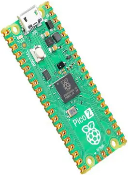
Raspberry Pi SC1631 Raspberry Microcontroller
Product Specifications
- Model: RP2350
- Package: QFN-60
- Internal Flash Storage: No
- Voltage Regulator: On-chip switching regulator
- Regulator Pins: 5 (3.3V input, 1.1V output, VREG_AVDD, VREG_LX, VREG_PGND)
Product Usage Instructions
- Chapter 1: Introduction
- The RP2350 series offers different package options compared to the RP2040 series. The RP2350A and RP2354A come in a QFN-60 package without and with internal flash storage respectively, while the RP2354B and RP2350B come in a QFN-80 package with and without flash storage.
- Chapter 2: Power
The RP2350 series features a new on-chip switching voltage regulator with five pins. This regulator requires external components for operation but offers higher power efficiency at higher load currents compared to the linear regulator in the RP2040 series. Pay attention to noise sensitivity in the VREG_AVDD pin that supplies the analogue circuitry.
Frequently Asked Questions (FAQ)
- Q: What is the main difference between RP2350A and RP2350B?
A: The main difference lies in the presence of internal flash storage. RP2350A does not have internal flash storage while RP2350B does. - Q: How many pins does the voltage regulator in the RP2350 series have?
A: The voltage regulator in the RP2350 series has five pins.
Hardware design with RP2350 Using RP2350 microcontrollers to build boards and products
Colophon
- © 2023-2024 Raspberry Pi Ltd
- This documentation is licensed under a Creative Commons Attribution-NoDerivatives 4.0 International (CC BY-ND). build-date: 2024-08-08 build-version: c0acc5b-clean
- Legal disclaimer notice
- TECHNICAL AND RELIABILITY DATA FOR RASPBERRY PI PRODUCTS (INCLUDING DATASHEETS) AS MODIFIED FROM TIME TO TIME (“RESOURCES”) ARE PROVIDED BY RASPBERRY PI LTD (“RPL”) “AS IS” AND ANY EXPRESS OR IMPLIED WARRANTIES, INCLUDING, BUT NOT LIMITED TO, THE IMPLIED WARRANTIES OF MERCHANTABILITY AND FITNESS FOR A PARTICULAR PURPOSE ARE DISCLAIMED. TO THE MAXIMUM EXTENT PERMITTED BY APPLICABLE LAW IN NO EVENT SHALL RPL BE LIABLE FOR ANY DIRECT, INDIRECT, INCIDENTAL, SPECIAL, EXEMPLARY, OR CONSEQUENTIAL DAMAGES (INCLUDING, BUT NOT LIMITED TO, PROCUREMENT OF SUBSTITUTE GOODS OR SERVICES; LOSS OF USE, DATA, OR PROFITS; OR BUSINESS INTERRUPTION) HOWEVER CAUSED AND ON ANY THEORY OF LIABILITY, WHETHER IN CONTRACT, STRICT LIABILITY, OR TORT (INCLUDING NEGLIGENCE OR OTHERWISE) ARISING IN ANY WAY OUT OF THE USE OF THE RESOURCES, EVEN IF ADVISED OF THE POSSIBILITY OF SUCH DAMAGE.
- RPL reserves the right to make any enhancements, improvements, corrections or any other modifications to the RESOURCES or any products described in them at any time and without further notice.
The RESOURCES are intended for skilled users with suitable levels of design knowledge. Users are solely responsible for their selection and use of the RESOURCES and any application of the products described in them. User agrees to indemnify and hold RPL harmless against all liabilities, costs, damages or other losses arising out of their use of the RESOURCES. - RPL grants users permission to use the RESOURCES solely in conjunction with the Raspberry Pi products. All other use of the RESOURCES is prohibited. No licence is granted to any other RPL or other third party intellectual property right.
- HIGH RISK ACTIVITIES. Raspberry Pi products are not designed, manufactured or intended for use in hazardous environments requiring fail safe performance, such as in the operation of nuclear facilities, aircraft navigation or communication systems, air traffic control, weapons systems or safety-critical applications (including life support systems and other medical devices), in which the failure of the products could lead directly to death, personal injury or severe physical or environmental damage (“High Risk Activities”). RPL specifically disclaims any express or implied warranty of fitness for High Risk Activities and accepts no liability for use or inclusions of Raspberry Pi products in High Risk Activities.
- Raspberry Pi products are provided subject to RPL’s Standard Terms. RPL’s provision of the RESOURCES does not expand or otherwise modify RPL’s Standard Terms including but not limited to the disclaimers and warranties expressed in them.
Chapter 1. Introduction
Figure 1. KiCad 3D rendering of the RP2350A Minimal design example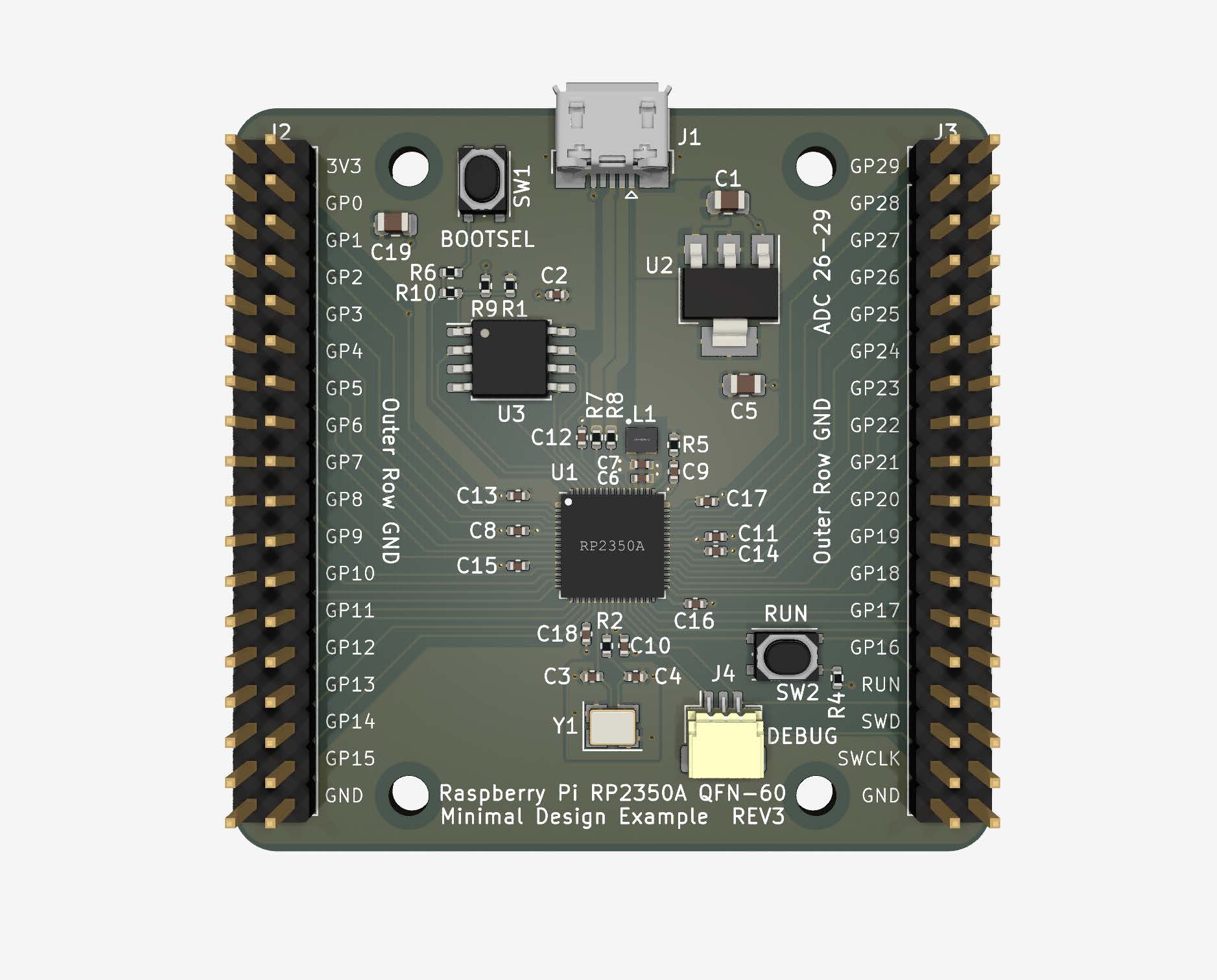
When we first introduced the Raspberry Pi RP2040, we also released a ‘Minimal’ design example and accompanying guide Hardware design with RP2040 which hopefully explained how the RP2040 could be used in a simple circuit board, and why the various component choices were made. With the arrival of the RP235x series, it’s time to revisit the original RP2040 Minimal design, and update it to account for the new features, and also for each of the package variants; the RP2350A with its QFN-60 package, and the RP2350B which is a QFN-80. Again, these designs are in Kicad (7.0) format, and are available to download (https://datasheets.raspberrypi.com/rp2350/Minimal-KiCAD.zip).
The Minimal Board
The original Minimal board was an attempt to provide a simple reference design, using the bare minimum of external components required to run the RP2040 and still have all the IO exposed and accessible. This was essentially comprised of a power source (a 5V to 3.3V linear regulator), crystal oscillator, flash memory, and IO connections (a micro USB socket and GPIO headers). The new RP235x series Minimal boards are largely the same, but with some changes necessary due to the new hardware. In addition to this, and despite going somewhat against the minimal nature of the design, I’ve added a couple of buttons for bootsel and run, together with a separate SWD header, which should mean a thoroughly less frustrating debug experience this time around. Designs don’t strictly speaking need these buttons, the signals are still available on the headers, and they can be omitted if you are particularly cost or space conscious, or have masochistic tendencies.
RP2040 vs RP235x series
The most obvious change is in the packages. Whereas the RP2040 is a 7x7mm QFN-56, the RP235x series currently has four different members. There are two devices which share the same QFN-60 package; the RP2350A which does not contain internal flash storage, and the RP2354A which does. Similarly, the QFN-80 also comes in two flavors; the RP2354B with flash, and RP2350B without. The QFN-60 devices and the original RP2040 share a common heritage.
They each have 30 GPIOs, four of which are also connected to the ADC, and are 7x7mm in size. Despite this, the RP2350A is not a drop-in replacement for the RP2040, as the number of pins on each is different. By contrast, the QFN-80 chips now have 48 GPIOs, and eight of these are now ADC capable. Because of this, we now have two Minimal boards; one for the 60 pin devices, and one for the 80. These Minimal boards are primarily designed for the parts without internal flash (RP2350), however the designs can easily be used with the internal flash devices (RP2354) by simply omitting the onboard flash memory, or even using it as a secondary flash device (more on this later). There is little difference between the two boards, other than the fact the QFN-80 version has longer rows of headers to accommodate the extra GPIO, and the board is therefore larger.
Aside from the package, the biggest board-level difference between the RP235x series and RP2040 are the power supplies. The RP235x series has some new power pins, and a different internal regulator. The 100mA linear regulator of the RP2040 has been replaced with a 200mA switching regulator, and as such, it requires some very specific circuitry, and no little care taken with the layout. It is highly recommended that you closely follow our layout and component selections; we’ve already gone through the pain of having to make several iterations of the design, so hopefully you don’t have to.
Figure 2. KiCad 3D rendering of the RP2350B Minimal design example 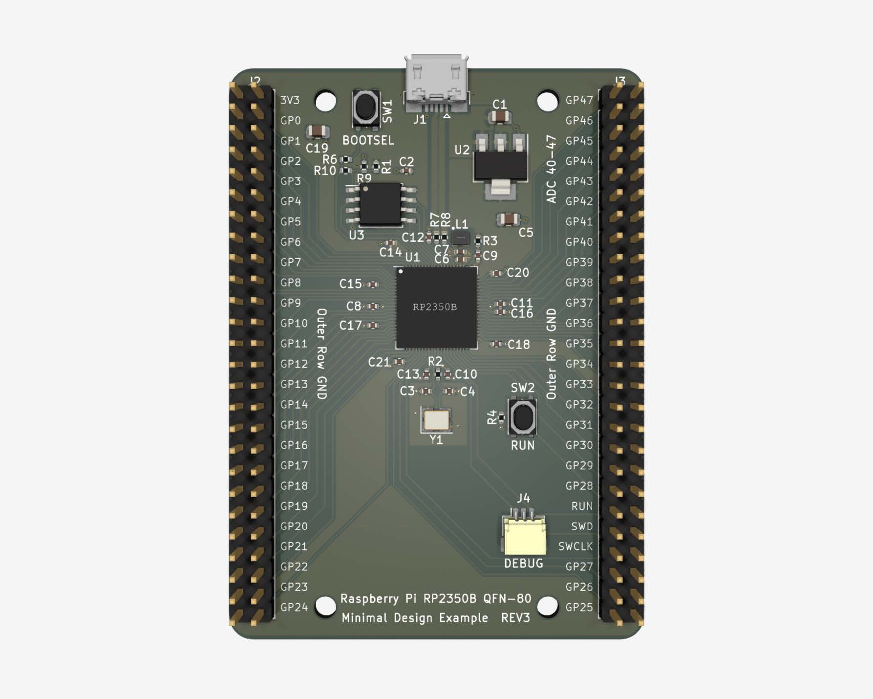
The Design
The intention of the Minimal design examples is to create a pair of simple boards using the RP235x series, which should be cheaply and easily manufacturable, without using unnecessarily exotic PCB technologies. The Minimal boards are therefore 2 layer designs, using components which should be commonly available, and all mounted on the top side of the board. While it would be nice to use large, easily hand-solder able components, the small pitch of the QFN chips (0.4mm) means that using some 0402 (1005 metric) passive components is unavoidable if all the GPIOs are to be used. While hand-soldering 0402 components isn’t too challenging with a decent soldering iron, it is very nearly impossible to solder the QFNs without specialist equipment.
Over the next few sections, I’m going to attempt to explain what the additional circuitry is for, and hopefully how we came to make the choices we did. As I’m actually going to be talking about two separate designs, one for each package size, I’ve tried to keep things as simple as I can. As far as is possible, all of the component references for the two boards are identical, so if I refer to U1, R1, etc, then it’s equally relevant to both boards. The obvious exception is when the component is only on one of the boards (in all cases, this will be on the larger 80 pin variant), then the component in question will only be on the QFN-80 design; for example, R13 only appears on this board.
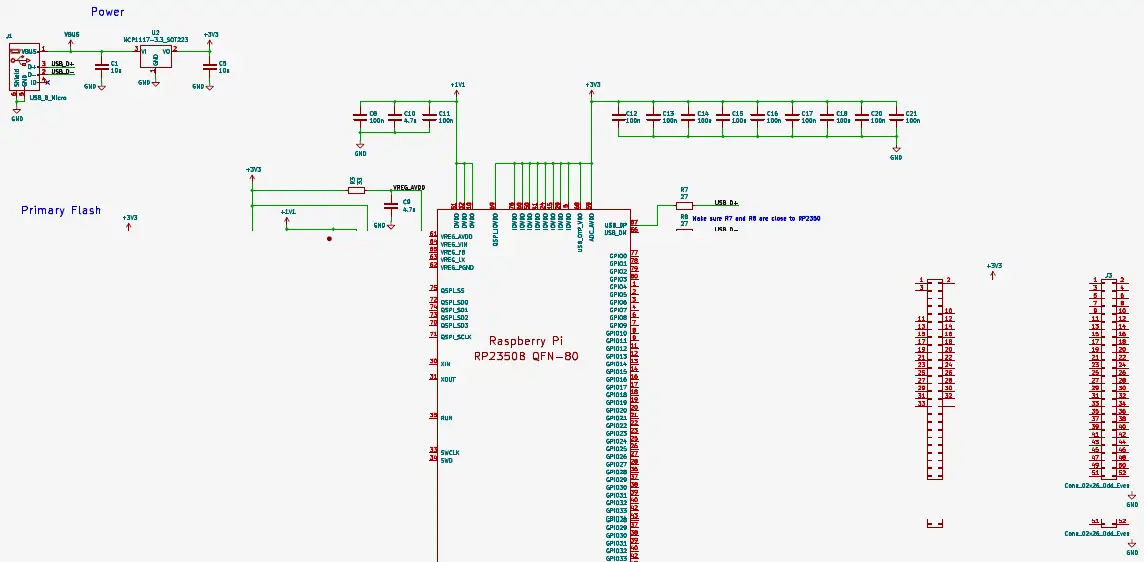
Chapter 2. Power
The power supplies of the RP235x series and the RP2040 differ somewhat this time around, though in its simplest configuration, it still requires two supplies, 3.3V and 1.1V. The RP235x series are simultaneously more power hungry, as it’s higher performance, and also more frugal (when in a low power state) than it’s predecessor, and so the linear regulator on the RP2040 has been upgraded with a switching regulator. This allows us greater power efficiency at higher currents (up to 200mA compared to the 100mA previously).
New on-chip voltage regulator
Figure 3. Schematic section showing the internal regulator circuit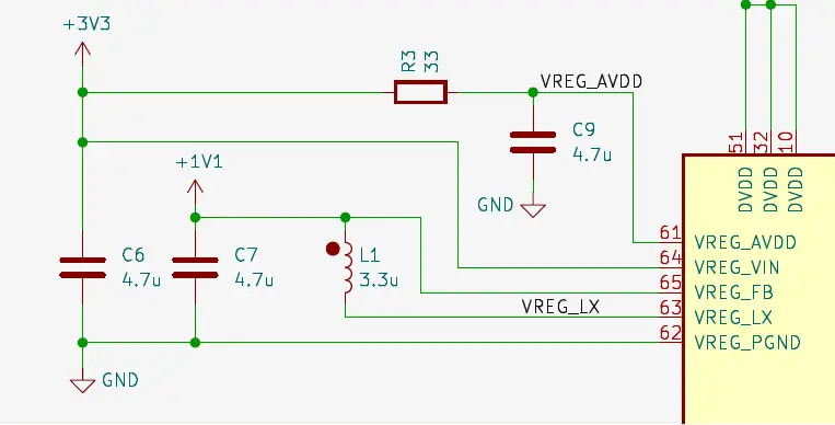
The linear regulator of the RP2040 had two pins, a 3.3V input, and a 1.1V output to supply the DVDD on the chip. This time, the regulator of the RP235x series has five pins, and requires some external componentry to make it work. While this seems a bit of a backward step in terms of usability, the switching regulator has the advantage of being more power efficient at higher load currents.
As the name suggests, the regulator rapidly switches on and off an internal transistor connecting the 3.3V input voltage (VREG_VIN) to the VREG_LX pin, and with the help of an inductor (L1) and an output capacitor (C7), it can produce a DC output voltage which has been stepped-down from the input. The VREG_FB pin monitors the output voltage, and adjusts the on/off ratio of the switching cycle, to ensure that the required voltage is maintained. As large currents are switched from VREG_VIN to VREG_LX, a large capacitor (C6) close to the input is required, so we don’t upset the 3.3V supply too much. Speaking of these large switching currents, the regulator also comes with its own ground return connection, VREG_PGND. Similarly with VREG_VIN and VREG_LX, the layout of this connection is critical, and while VREG_PGND must connect to the main GND, it must be done in such a way that all the large switching currents return directly to the PGND pin, without disturbing the rest of the GND too much.
The last pin is VREG_AVDD, which supplies the analogue circuitry within the regulator, and this is very sensitive to noise.
Figure 4. Schematic section showing the PCB layout of the regulator 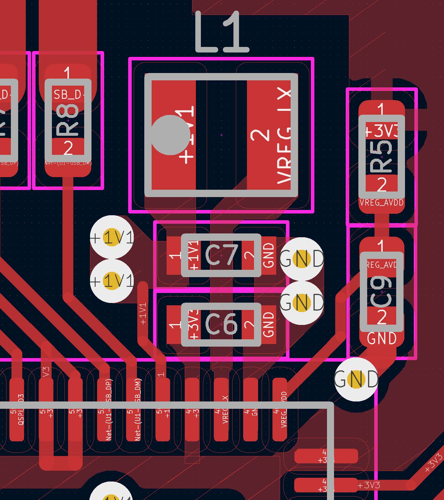
- The layout of the regulator on the minimal boards closely mirrors that of the Raspberry Pi Pico 2. A great deal of work has gone into the design of this circuit, with many iterations of the PCB required in order to make it as good as we possibly can. While you could place these components in a variety of different ways and still get the regulator to ‘work’ (ie, produce an output voltage at roughly the right level, good enough to get it running code), we’ve found that our regulator needs to be treated in exactly the right way to keep it happy, and by happy, I mean producing the correct output voltage under a range of load current conditions.
- While performing our experiments on this, we were somewhat disappointed to be reminded that the inconvenient world of physics cannot always be ignored. We, as engineers, largely try and do exactly this; simplifying components, ignoring (often) insignificant physical properties, and instead focusing on the property that we’re interested in. For example, a simple resistor does not just have a resistance, but also inductance, etc. In our case, we (re)discovered that inductors have a magnetic field associated with them, and importantly, radiates in a direction depending on which way the coil is wound, and the direction of the flow of the current. We were also reminded that a ‘fully’ shielded inductor doesn’t mean what you think it might. The magnetic field is attenuated to a large extent, but some does still escape. We found that the regulator performance could be massively improved if the inductor is ‘the right way round’.
- It turns out that the magnetic field emitting from a ‘wrong way round’ inductor interferes with the regulator output capacitor (C7), which in turn upsets the control circuitry within RP2350. With the inductor in the proper orientation, and the precise layout and component selections used here, then this problem goes away. There will undoubtedly be other layouts, components, etc, which could work with an inductor in any orientation, but they will most likely use a lot more PCB space in order to do so. We have provided this recommended layout to save people the many engineering hours we have spent developing and refining this compact and well-behaved solution.
- More to the point, we’re going so far as saying that if you choose not to use our example, then you do so at your own risk. Much like we already do with RP2040 and the crystal circuit, where we insist (well, strongly suggest) you use a particular part (we will do so again in the crystal section of this document).
- The directionality of these small inductors is pretty much universally ignored, with the orientation of the coil winding impossible to deduce, and also randomly distributed along a reel of components. Larger inductor case sizes can often be found to have polarity markings on them, however we could find no suitable ones in the 0806 (2016 metric) case size we have chosen. To this end, we have worked with Abracon to produce a 3.3μH part with a dot to indicate polarity, and importantly, come on a reel with them all aligned the same way. The TBD are (or will very shortly) be made available to the general public from distributers. As mentioned earlier, the VREG_AVDD supply is very sensitive to noise, and therefore needs to be filtered. We found that as the VREG_AVDD only draws around 200μA, an RC filter of 33Ω and 4.7μF is adequate.
- So, to recap, the components used will be…
- C6, C7 & C9 – 4.7μF (0402, 1005 metric)
- L1 – Abracon TBD (0806, 2016 metric)
- R3 – 33Ω (0402, 1005 metric)
- The RP2350 datasheet has a more detailed discussion on the regulator layout recommendations, please see External Components and PCB layout requirements.
Input supply
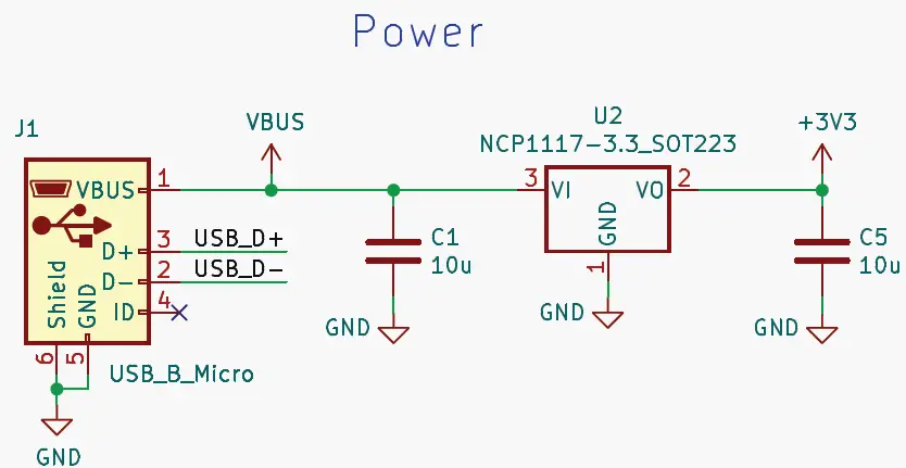
The input power connection for this design is via the 5V VBUS pin of a Micro-USB connector (labelled J1 in Figure 5). This is a common method of powering electronic devices, and it makes sense here, as RP2350 has USB functionality, which we will be wiring to the data pins of this connector. As we need only 3.3V for this design (the 1.1V supply comes from the internal), we need to lower the incoming 5V USB supply, in this case, using another, external voltage regulator, in this case a linear regulator (a.k.a Low Drop Out regulator, or LDO). Having previously extolled the virtues of using an efficient switching regulator, it could also be a wise choice to use one here as well, but I’ve opted for simplicity. Firstly, using an LDO is almost always easier. There’s no calculations required to figure out what size inductor you should use, or how big are the output capacitors, and the layout is usually a lot more straightforward too. Secondly, saving every last drop of power isn’t the aim here; if it was, I’d seriously consider using a switching regulator, and you can find an example of doing so on the Raspberry Pi Pico 2. And thirdly, I can simply ‘borrow’ the circuit I previously used on the RP2040 version of the Minimal board. The NCP1117 (U2) chosen here has a fixed output of 3.3V, is widely available, and can provide up to 1A of current, which will be plenty for most designs. A look at the datasheet for the NCP1117 tells us that this device requires a 10μF capacitor on the input, and another on the output (C1 and C5).
Decoupling capacitors
Figure 6. Schematic section showing the RP2350 power supply inputs, voltage regulator and decoupling capacitors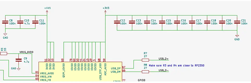
Another aspect of the power supply design are the decoupling capacitors required for RP2350. These provide two basic functions. Firstly, they filter out power supply noise, and secondly, provide a local supply of charge that the circuits inside RP2350 can use at short notice. This prevents the voltage level in the immediate vicinity from dropping too much when the current demand suddenly increases. Because, of this, it is important to place decoupling close to the power pins. Ordinarily, we recommend the use of a 100nF capacitor per power pin, however, we deviate from this rule in a couple of instances.
Figure 7. Section of layout showing RP2350 routing and decoupling 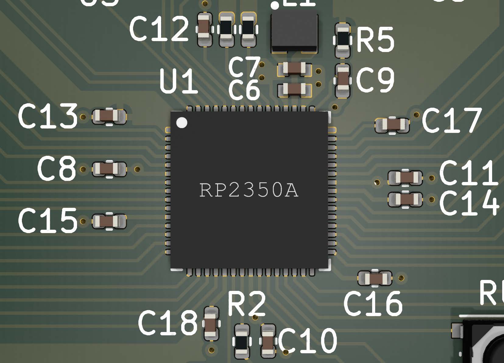
- Firstly, in order to be able to have enough space for all of the chip pins to be able to be routed out, away from the device, we have to compromise with the amount of decoupling capacitors we can use. In this design, pins 53 and 54 of RP2350A (pins 68 and 69 of RP2350B) share a single capacitor (C12 in Figure 7 and Figure 6), as there is not a lot of room on that side of the device, and the components and layout of the regulator take precedence.
- This lack of space could be somewhat overcome if we used more complex/expensive technology, such as smaller components, or a four layer PCB with components on both the top and bottom sides. This is a design trade-off; we have decreased the complexity and cost, at the expense of having less decoupling capacitance, and capacitors which are slightly further away from the chip than is optimal (this increases the inductance). This could have the effect of limiting the maximum speed the design could operate at, as the voltage supply could get too noisy and drop below the minimum allowed voltage; but for most applications, this trade-off should be acceptable.
- The other deviation from the 100nF rule is so we can further improve the voltage regulator performance; we recommend using a 4.7μF for C10, which is the placed on the other side of the chip from the regulator.
Chapter 3. Flash Memory
Primary flash
Figure 8. Schematic section showing the primary flash memory and USB_BOOT circuitry
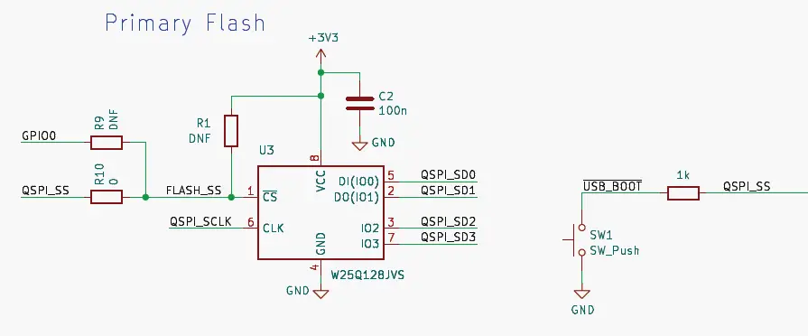
- In order to be able to store program code which RP2350 can boot and run from, we need to use a flash memory, specifically, a quad SPI flash memory. The device chosen here is an W25Q128JVS device (U3 in the Figure 8), which is a 128Mbit chip (16MB). This is the largest memory size that RP2350 can support. If your particular application doesn’t need as much storage, then a smaller, cheaper memory could be used instead.
- As this databus can be quite high frequency and is regularly in use, the QSPI pins of RP2350 should be wired directly to the flash, using short connections to maintain the signal integrity, and to also reduce crosstalk in surrounding circuits. Crosstalk is where signals on one circuit net can induce unwanted voltages on a neighbouring circuit, potentially causing errors to occur.
- The QSPI_SS signal is a special case. It is connected to the flash directly, but it also has two resistors (well, four, but I’ll come on to that later) connected to it. The first (R1) is a pull-up to the 3.3V supply. The flash memory requires the chip-select input to be at the same voltage as its own 3.3V supply pin as the device is powered up, otherwise, it does not function correctly. When the RP2350 is powered up, its QSPI_SS pin will automatically default to a pull-up, but there is a short period of time during switch-on where the state of the QSPI_SS pin cannot be guaranteed. The addition of a pull-up resistor ensures that this requirement will always be satisfied. R1 is marked as DNF (Do Not Fit) on the schematic, as we have found that with this particular flash device, the external pull-up is unnecessary. However, if a different flash is used, it may become important to be able to insert a 10kΩ resistor here, so it has been included just in case.
- The second resistor (R6) is a 1kΩ resistor, connected to a push button (SW1) labelled ‘USB_BOOT’. This is because the QSPI_SS pin is used as a ‘boot strap’; RP2350 checks the value of this I/O during the boot sequence, and if it is found to be a logic 0, then RP2350 reverts to the BOOTSEL mode, where RP2350 presents itself as a USB mass storage device, and code can be copied directly to it. If we simply press the button, we pull QSPI_SS pin to ground, and if the device is then subsequently reset (e.g. by toggling the RUN pin), RP2350 will restart in BOOTSEL mode instead of attempting to run the contents of the flash. These resistors, R2 and R6 (R9 and R10 also), should be placed close to the flash chip, so we avoid additional lengths of copper tracks which could affect the signal.
- All of the above specifically applies to the RP2350, which has no internal flash. Of course, the RP2354 devices have internal 2MB flash memories, so the external U3 memory is not required, so U3 can safely be removed from the schematic, or simply left unpopulated. In either of these cases, we would still want to keep the USB_BOOT switch connected to QSPI_SS, so that we can still enter USB boot mode.
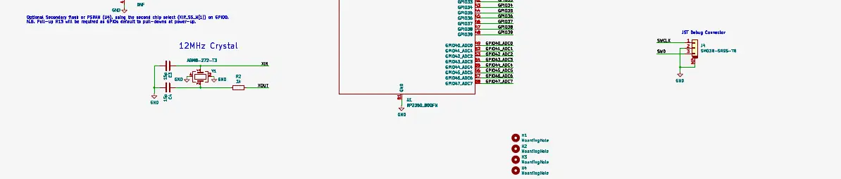
Secondary flash or PSRAM
- The RP235x series now supports a second memory device using the same QSPI pins, with a GPIO providing the additional chip select. So, if we are using an RP2354 (which has internal flash), then we could use U3 as a secondary flash, or even replace it with a PSRAM device. In order to do this, we need to disconnect QSPI_SS from U3, and instead connect it to a suitable GPIO instead. The nearest GPIO capable of being a chip select (XIP_CS1n) is GPIO0, so by removing the 0Ω from R10, and fitting it to R9, we can now access U3 in addition to the on-chip flash. In order to fully take advantage of this feature, where we have two external memory devices so that the flash-less RP2350 parts can benefit, the larger of the two Minimal boards, for the RP2350B, includes an optional footprint (U4) for an additional memory chip.
Figure 9. Schematic section showing the optional secondary memory device
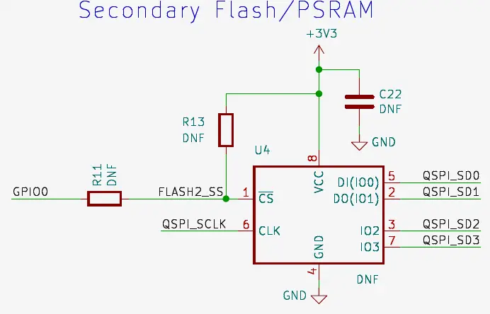
To be able to use this device, it will obviously have to be populated , as well as R11 (0Ω), and R13 (10KΩ). The addition of R11 connects GPIO0 (the XIP_CS1n signal) to the chip select of the second memory. The pull-up on the chip select pin is definitely needed this time, as the default state of GPIO0 is to be pulled low at power-up, which would cause our flash device to fail. C22 would also be needed to provide local power supply decoupling for U4.
Supported flash chips
The initial flash probe sequence, used by the bottom to extract the second stage from flash, uses an 03h serial read command, with 24-bit addressing, and a serial clock of approximately 1MHz. It repeatedly cycles through the four combinations of clock polarity and clock phase, looking for a valid second stage CRC32 checksum.
As the second stage is then free to configure execute-in-place using the same 03h serial read command, RP2350 can perform cached flash execute-in-place with any chip supporting 03h serial read with 24-bit addressing, which includes most 25-series flash devices. The SDK provides an example second stage for CPOL=0 CPHA=0, at https://github.com/raspberrypi/pico-sdk/blob/master/src/rp2350/boot_stage2/boot2_generic_03h.S. To support flash programming using the routines in the bottom , the device must also respond to the following commands:
- 02h 256-byte page program
- 05h status register read
- 06h set write enable latch
- 20h 4kB sector erase
RP2350 also supports a wide variety of dual-SPI and QSPI access modes. For example, https://github.com/raspberrypi/pico-sdk/blob/master/src/rp2350/boot_stage2/boot2_w25q080.S configures a Winbond W25Q-series device for quad-IO continuous read mode, where RP2350 sends quad-IO addresses (without a command prefix) and the flash responds with quad-IO data.
Some caution is needed with flash XIP modes where the flash device stops responding to standard serial commands, like the Winbond continuous read mode mentioned above. This can cause issues when RP2350 is reset, but the flash device is not power-cycled, because the flash will then not respond to the bootrom’s flash probe sequence. Before issuing the 03h serial read, the bootrom always issues the following fixed sequence, which is a best-effort sequence for discontinuing XIP on a range of flash devices:
- CSn=1, IO[3:0]=4’b0000 (via pull downs to avoid contention), issue ×32 clocks
- CSn=0, IO[3:0]=4’b1111 (via pull ups to avoid contention), issue ×32 clocks
- CSn=1
- CSn=0, MOSI=1’b1 (driven low-Z, all other I/Os Hi-Z), issue ×16 clocks
If your chosen device does not respond to this sequence when in its continuous read mode, then it must be kept in a state where each transfer is prefixed by a serial command, otherwise RP2350 will not be able to recover following an internal reset.
For more details on the QSPI , please see QSPI Memory Interface (QMI) in the RP2350 datasheet.
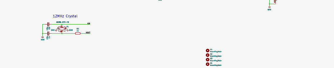
Chapter 4. Crystal Oscillator
Figure 10. Schematic section showing the crystal oscillator and load capacitors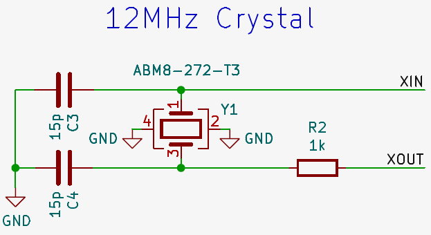
- Strictly speaking, RP2350 does not actually require an external clock source, as it has its own internal oscillator. However, as the frequency of this internal oscillator is not well defined or controlled, varying from chip to chip, as well as with different supply voltages and temperatures, it is recommended to use a stable external frequency source. Applications which rely on exact frequencies are not possible without an external frequency source, USB being a prime example.
- Providing an external frequency source can be done in one of two ways: either by providing a clock source with a CMOS output (square wave of IOVDD voltage) into the XIN pin, or by using a 12MHz crystal connected between
- XIN and XOUT. Using a crystal is the preferred option here, as they are both relatively cheap and very accurate.
- The chosen crystal for this design is an ABM8-272-T3 (Y1 in Figure 10). This is the same 12MHz crystal used on the Raspberry Pi Pico and Raspberry Pi Pico 2. We highly recommend using this crystal along with the accompanying circuitry to ensure that the clock starts quickly under all conditions without damaging the crystal itself. The crystal has a 30ppm frequency tolerance, which should be good enough for most applications. Along with a frequency tolerance of+/-30ppm, it has a maximum ESR of 50Ω, and a load capacitance of 10pF, both of which had a bearing on the choice of accompanying components.
- For a crystal to oscillate at the desired frequency, the manufacturer specifies the load capacitance that it needs for it to do so, and in this case, it is 10pF. This load capacitance is achieved by placing two capacitors of equal value, one on each side of the crystal to ground (C3 and C4). From the crystal’s point of view, these capacitors are connected in series between its two terminals. Basic circuit theory tells us that they combine to give a capacitance of (C3*C4)/(C3+C4), and as C3=C4, then it is simply C3/2. In this example, we’ve used 15pF capacitors, so the series combination is 7.5pF. In addition to this intentional load capacitance, we must also add a value for the unintentional extra capacitance, or parasitic capacitance, that we get from the PCB tracks and the XIN and XOUT pins of RP2350. We’ll assume a value of 3pF for this, and as this capacitance is in parallel to C3 and C4, we simply add this to give us a total load capacitance of 10.5pF, which is close enough to the target of 10pF. As you can see, the parasitic capacitance of the PCB traces are a factor, and we therefore need to keep them small so we don’t upset the crystal and stop it oscillating as intended. Try and keep the layout as short as possible.
- The second consideration is the maximum ESR (equivalent series resistance) of the crystal. We’ve opted for a device with a maximum of 50Ω, as we’ve found that this, along with a 1kΩ series resistor (R2), is a good value to prevent the crystal being over-driven and being damaged when using an IOVDD level of 3.3V. However, if IOVDD is less than 3.3V, then the drive current of the XIN/XOUT pins is reduced, and you will find that the amplitude of the crystal is lower, or may not even oscillate at all. In this case, a smaller value of the series resistor will need to be used. Any deviation from the crystal circuit shown here, or with an IOVDD level other than 3.3V, will require extensive testing to ensure that the crystal oscillates under all conditions, and starts-up sufficiently quickly as not to cause problems with your application.
Recommended crystal
- For original designs using RP2350 we recommend using the Abracon ABM8-272-T3. For example, in addition to the minimal design example, see the Pico 2 board schematic in Appendix B of the Raspberry Pi Pico 2 Datasheet and the Pico 2 design files.
- For the best performance and stability across typical operating temperature ranges, use the Abracon ABM8-272-T3. You can source the ABM8-272-T3 directly from Abracon or from an authorised reseller. Pico 2 has been specifically tuned for the ABM8-272-T3, which has the following specifications:
- Even if you use a crystal with similar specifications, you will need to test the circuit over a range of temperatures to ensure stability.
- The crystal oscillator is powered from the IOVDD voltage. As a result, the Abracon crystal and that particular damping resistor are tuned for 3.3V operation. If you use a different IO voltage, you will need to re-tune.
- Any changes to crystal parameters risk instability across any components connected to the crystal circuit.
- If you can’t source the recommended crystal directly from Abracon or a reseller, contact applications@raspberrypi.com.
Chapter 5. IOs
USB
Figure 11. Schematic section showing the USB pins of RP2350 and series termination
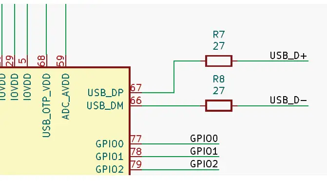
- The RP2350 provides two pins to be used for full speed (FS) or low speed (LS) USB, either as a host or device, depending on the software used. As we’ve already discussed, RP2350 can also boot as a USB mass storage device, so wiring up these pins to the USB connector (J1 in Figure 5) makes sense. The USB_DP and USB_DM pins on RP2350 do not require any additional pull-ups or pull-downs (required to indicate speed, FS or LS, or whether it is a host or device), as these are built in to the I/Os. However, these I/Os do require 27Ω series termination resistors (R7 and R8 in Figure 11), placed close to the chip, in order to meet the USB impedance specification.
- Even though RP2350 is limited to full speed data rate (12Mbps), we should try and makes sure that the characteristic impedance of the transmission lines (the copper tracks connecting the chip to the connector) are close to the
- USB specification of 90Ω (measured differentially). On a 1mm thick board such as this, if we use 0.8mm wide tracks on USB_DP and USB_DM, with a gap of 0.15mm between them, we should get a differential characteristic impedance of around 90Ω. This is to ensure that the signals can travel along these transmission lines as cleanly as possible, minimising voltage reflections which can reduce the integrity of the signal. In order for these transmission lines to work properly, we need to make sure that directly below these lines is a ground. A solid, uninterrupted area of ground copper, stretching the entire length of the track. On this design, almost the entirety of the bottom copper layer is devoted to ground, and particular care was taken to ensure that the USB tracks pass over nothing but ground. If a PCB thicker than 1mm is chosen for your build, then we have two options. We could re-engineer the USB transmission lines to compensate for the greater distance between the track and ground underneath (which could be a physical impossibility), or we could ignore it, and hope for the best. USB FS can be quite forgiving, but your mileage may vary. It is likely to work in many applications, but it’s probably not going to be compliant to the USB standard.
I/O headers
Figure 12. Schematic section showing the 2.54mm I/O headers of the QFN60 version
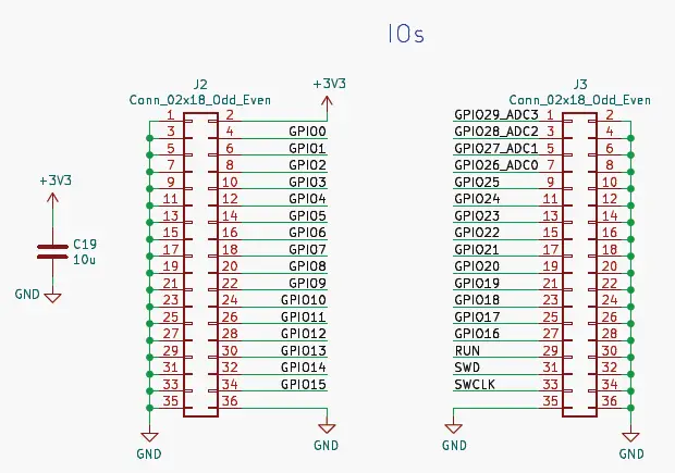
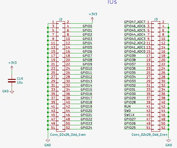
- In addition to the USB connector already mentioned, there are a pair of dual row 2.54mm headers (J2 and J3 in Figure 12), one on each side of the board, to which the rest of the I/O have been connected. There are 30 GPIO on the RP2350A, whereas there are 48 GPIO on the RP2350B, so the headers on this version of the Minimal board are larger to allow for the extra pins (see Figure 13).
- As this is a general purpose design, with no particular application in mind, the I/O have been made available to be connected as the user wishes. The inner row of pins on each header are the I/Os, and the outer row are all connected to ground. It is good practice to include many grounds on I/O connectors. This helps to maintain a low impedance ground, and also to provide plenty of potential return paths for currents travelling to and from the
- I/O connections. This is important to minimise electro-magnetic interference which can be caused by the return currents of quickly switching signals taking long, looping paths to complete the circuit.
- Both headers are on the same 2.54mm grid, which makes connecting this board to other things, such as breadboards, easier. You might want to consider fitting only a single row header instead of the dual row header, dispensing with the outer row of ground connections, to make it more convenient to fit to a breadboard.
Figure 13. Schematic section showing the 2.54mm I/O headers of the QFN80 version
Debug connector
Figure 14. Schematic section showing the optional JST connector for SWD debug
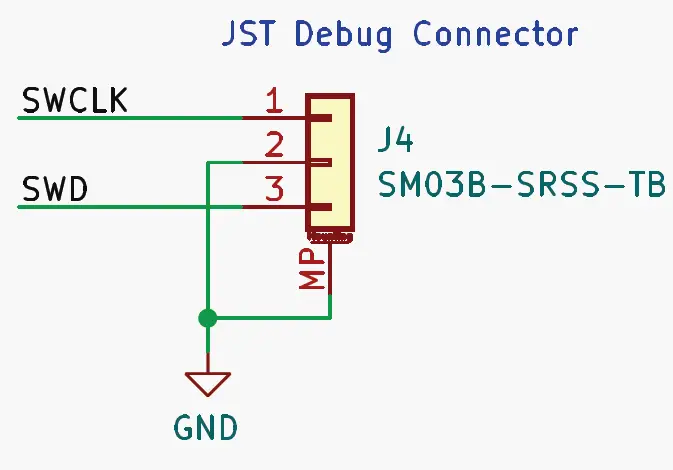
For on-chip debugging, you may wish to connect to the SWD interface of the RP2350. The two pins, SWD and SWCLK, are available on the 2.54mm header, J3, to allow the debug probe of your choice to be easily connected. In addition to this, I’ve included an optional JST header, which allows an easy connection to Raspberry Pi Debug Probe. You don’t need to use this, the 2.54mm headers will suffice if you do intend to debug software, but I find it more convenient to do so. I’ve chosen a horizontal connector, mostly because I like the look of it, even if it’s not on the edge of the board, but vertical ones are available, albeit with a slightly different footprint.
Buttons
The Minimal design now contains not one, but two buttons, where the RP240 version had none. One is for USB boot selection as we’ve previously discussed, but the second is a ‘reset’ button, hooked up to the RUN pin. Neither of these are strictly necessary (though the BOOTSEL button would have to be replaced with a header or similar if USB boot mode was required), and can be removed if space or cost is a concern, but they certainly make using the RP2350 a far more pleasant experience.
Appendix A: Complete Schematic -RP2350A version
Figure 15. Full schematic of the Minimal Design for RP2350A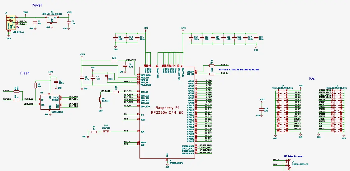
Appendix B: Complete Schematic -RP2350B version
Figure 16. Full schematic of the Minimal Design for RP2350B
Appendix H: Documentation Release History
August 8 2024
Initial release.
i Raspberry Pi
Raspberry Pi is a trademark of Raspberry Pi Ltd
Raspberry Pi Ltd
Documents / Resources
 |
Raspberry Pi SC1631 Raspberry Microcontroller [pdf] Instruction Manual SC1631 Raspberry Microcontroller, SC1631, Raspberry Microcontroller, Microcontroller |


