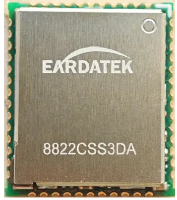
EARDATEK EWN-8822CSS3DA WiFi and BT Combo Module
Specifications
- Product Name: Ff Wi-Fi Module EWN-8822CSS3DA
- Wireless Standards: IEEE 802.11b/g/n/a/ac
- Wireless Interface: SDIO
- Bluetooth Versions: 2.1/3.0/4.2/5.0
- Wireless Data Rates: Up to 173.3 Mbps (20 MHz), 400 Mbps (40 MHz), 866.7 Mbps (80 MHz)
Product Usage Instructions
Installation
Insert the module into the appropriate slot on your device. Ensure proper alignment and secure the module in place.
Connection Setup
Power on your device and locate the Wi-Fi and Bluetooth settings.
Enable Wi-Fi and Bluetooth functionalities on your device.
Scan for available networks and select the desired network to connect.
Configuration
Configure Wi-Fi settings such as SSID, password, and encryption type.
Pair Bluetooth devices by following the device pairing instructions.
Troubleshooting
If you encounter connectivity issues, try resetting the module and re-establishing the connections.
Frequently Asked Questions (FAQ)
- Q: How do I update the firmware of the Ff Wi-Fi Module?
A: Firmware updates can be done by visiting the manufacturer’s website and following the provided instructions for updating the module. - Q: Can the Ff Wi-Fi Module be used with both Windows and Mac operating systems?
A: Yes, the Ff Wi-Fi Module is compatible with both Windows and Mac operating systems, given that the necessary drivers are installed.
E-mail: sales@eardatek.com
Earda Technologies Co., Ltd
General Specifications
The module provides a complete solution for a high-performance integrated wireless and Bluetooth device . It provides SDIO interface for WiFi and HS-UART interface for Bluetooth. The module complies with IEEE 802.11 a/b/g/n/ac 2T2R MIMO standard , and Maximum PHY data rate up to 173.3 Mbps using 20 MHz bandwidth ,400 Mbps using 40 MHz bandwidth, and 866.7 Mbps using 80 MHz bandwidth.
Features
WLAN
- Supports 802.11ac 2×2, Wave-2 compliant with MU-MIMO
- Completes 802.11n MIMO solution for 2.4GHz and 5GHz band
- Maximum PHY data rate up to 173.3Mbps using 20MHz bandwidth, 400Mbps using 40 MHz bandwidth, and 866.7Mbps using 80MHz bandwidth
- Backward compatible with 802.11a/b/g devices while operating at 802.11n data rates
- Backward compatible with 802.11a/n devices while operating at 802.11ac data rates
- Complies with SDIO 1.1/2.0/3.0 for WLAN with clock rate up to 208MHz
- support standard SDIO v3.0 (up to SDR104 mode at 208 MHz) host interfaces
- complies with HS-UART with configurable baud rate for Bluetooth
- IEEE 802.11a/b/g/n/ac compatible WLAN
- IEEE 802.11e QoS Enhancement(WMM)
- IEEE 802.11i (WPA, WPA2). Open, shared key and pair-wise key authentication
- IEEE 802.11h DFS, TPC, Spectrum Measurement
- IEEE 802.11k Radio Resource Measurement
- Channel management and co-existence
- Wi-Fi Direct supports wireless peer to peer
- CCA on secondary through RTS/CTS handshake
- Supports TCP/UDP/IP checksum offload
- Two Transmit and Two Receive paths
- 5MHz/10MHz/20MHz/40MHz/80MHz bandwidth transmission
- Supports 2.4GHz and 5GHz band channels
- Short Guard Interval(400ns)
- Sounding packet
Bluetooth
- Compatible with Bluetooth v2.1 and v3.0 Systems
- Supports Bluetooth 4.1 features
- Supports Bluetooth 4.2 LE Secure Connection by upper layer software upgrade
- Support Bluetooth 5.0 and LE 5.0 system
- Supports all packet types in basic rate and enhanced data rate
- Supports pico-nets in a scatter-net
- Supports Secure Simple Pairing
- Bluetooth 5.0 Dual Mode support: Simultaneous LE and BR/EDR
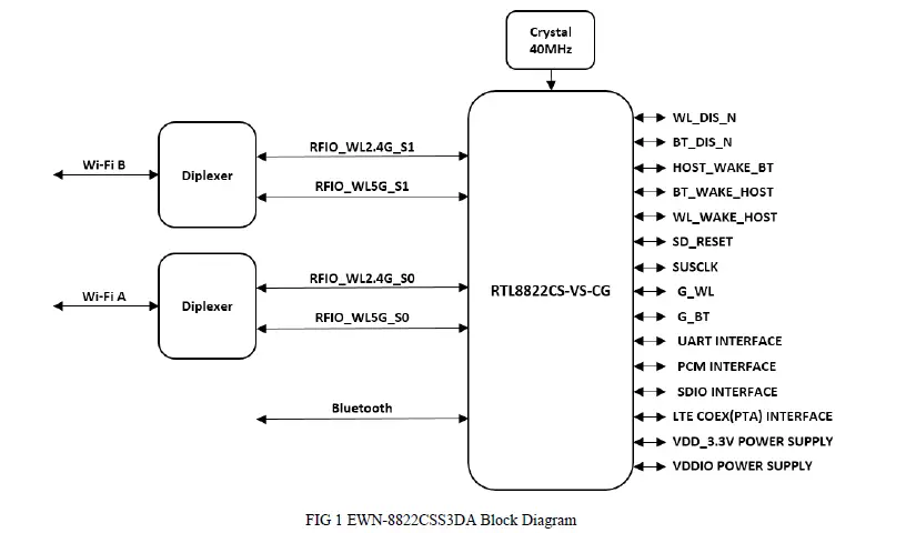
System Block Diagram
PHY Specification
Wi-Fi Specification
Table 1 EWN-8822CSS3DA Wi-Fi RF Parameters
| Protocol | IEEE 802.11b/g/n/a/ac | |
| Interface | SDIO 1.1 / 2.0 / 3.0 | |
| 2.4GHz band CH1~CH13/2400-2483.5MHz | ||
| Frequency | 5GHz Band CH36~CH48/5150-5250MHz CH52~CH64/5250-5350MHz CH100~CH144/5470-5725MHz CH149~CH165/5725-5850MHz |
|
| 2.4G&5G Band Refer to Channel Plan Domain Code | ||
| Bandwidth | 20/40/80 MHz | |
| Maximum PHY data rate up to 173.3 Mbps using 20MHz bandwidth; | ||
| PHY Rate | Maximum PHY data rate up to 400 Mbps using 40MHz bandwidth; | |
| Maximum PHY data rate up to 866.7 Mbps using 80MHz bandwidth . | ||
| Frequency Error | <±10ppm/802.11b/g/n/a/ac | |
| -20dB/±11MHz/OFDM; | ||
| Mask | -28dB/±20MHz/OFDM; | |
| -30dB/±11MHz/DSSS, CCK; | ||
| -50dB/±20MHz/DSSS, CCK. | ||
| 802.11b (2.4G 11Mbps): | 18 +1/-2dBm | |
| 2.4G Transmit Power |
802.11g (2.4G 54Mbps): | 17 +1/-2dBm |
| 802.11n (2.4G HT20 MCS7): | 16 +1/-2dBm | |
| 802.11n (2.4G HT40 MCS7): | 16 +1/-2dBm | |
| If customer needs to PASS the FCC certification, the 2.4G Tx power needs to be reduced to the following level by “ power limit table” | ||
| 802.11b (2.4G CCK): | 18 +1/-2dBm | |
| 802.11g (2.4G OFDM): | 16 +1/-2dBm | |
| 802.11n (2.4G HT20): | 11 +1/-2dBm | |
| 802.11n (2.4G HT40): | 11 +1/-2dBm | |
| Other TX power rate see the “power by rate” | ||
| 2.4G EVM | 802.11b (2.4G 1Mbps): | ≤-13dB |
| 802.11b (2.4G 11Mbps): | ≤-13dB | |
| 802.11g (2.4G 6Mbps): | ≤-8dB | |
| 802.11g (2.4G 24Mbps): | ≤-19dB | |
| 802.11g (2.4G 54Mbps): | ≤-28dB | |
| 802.11n (2.4G HT20 MCS0): | ≤-8dB | |
| 802.11n (2.4G HT20 MCS4): | ≤-22dB | |
| 802.11n (2.4G HT20 MCS7): | ≤-30dB | |
| 802.11n (2.4G HT40 MCS0): | ≤-8dB | |
| 802.11n (2.4G HT40 MCS4): | ≤-22dB | |
| 802.11n (2.4G HT40 MCS7): | ≤-30dB | |
| 5G Transmit Power5G EVM
|
802.11a (5G 54Mbps): | 17 +1/-2dBm |
| 802.11n (5G HT20 MCS7): | 16 +1/-2dBm | |
| 802.11n (5G HT40 MCS7): | 16 +1/-2dBm | |
| 802.11ac (5G VHT20 MCS8): | 14 +1/-2dBm | |
| 802.11ac (5G VHT40 MCS9): | 14 +1/-2dBm | |
| 802.11ac (5G VHT80 MCS9): | 14 +1/-2dBm | |
| Other TX power rate see the “power by rate” | ||
| 802.11a (5G 6Mbps): | ≤-8dB | |
| 802.11a (5G 24Mbps): | ≤-19dB | |
| 802.11a (5G 54Mbps): | ≤-28dB | |
| 802.11n (5G HT20 MCS0): | ≤-8dB | |
| 802.11n (5G HT20 MCS4): | ≤-22dB | |
| 802.11n (5G HT20 MCS7): | ≤-30dB | |
| 802.11n (5G HT40 MCS0): | ≤-8dB | |
| 802.11n (5G HT40 MCS4): | ≤-22dB | |
| 802.11n (5G HT40 MCS7): | ≤-30dB | |
| 802.11ac (5G VHT20 MCS0): | ≤-8dB | |
| 802.11ac (5G VHT20 MCS5): | ≤-25dB | |
| 802.11ac (5G VHT20 MCS8): | ≤-33dB | |
| 802.11ac (5G VHT40 MCS0): | ≤-8dB | |
| 802.11ac (5G VHT40 MCS5): | ≤-25dB | |
| 802.11ac (5G VHT40 MCS9): | ≤-35dB | ||
| 802.11ac (5G VHT80 MCS0): | ≤-8dB | ||
| 802.11ac (5G VHT80 MCS5): | ≤-25dB | ||
| 802.11ac (5G VHT80 MCS9): | ≤-35dB | ||
| 802.11b (2.4G 1Mbps): | -91dBm (Max.) | -97dBm (Typ.) | |
| 802.11b (2.4G 11Mbps): | -85dBm (Max.) | -93dBm (Typ.) | |
| 802.11g (2.4G 6Mbps): | -87dBm (Max.) | -96dBm (Typ.) | |
| 802.11g (2.4G 24Mbps): | -79dBm (Max.) | -83dBm (Typ.) | |
| 2.4G Receive Sensitivity @ PER<10% |
802.11g (2.4G 54Mbps): | -70dBm (Max.) | -77dBm (Typ.) |
| 802.11n (2.4G HT20 MCS0): | -87dBm (Max.) | -95dBm (Typ.) | |
| 802.11n (2.4G HT20 MCS4): | -75dBm (Max.) | -80dBm (Typ.) | |
| 802.11n (2.4G HT20 MCS7): | -69dBm (Max.) | -77dBm (Typ.) | |
| 802.11n (2.4G HT40 MCS0): | -84dBm (Max.) | -92dBm (Typ.) | |
| 802.11n (2.4G HT40 MCS4): | -72dBm (Max.) | -76dBm (Typ.) | |
| 802.11n (2.4G HT40 MCS7): | -66dBm (Max.) | -71dBm (Typ.) | |
| 802.11a (5G 6Mbps): | -87dBm (Max.) | -94dBm (Typ.) | |
| 802.11a (5G 24Mbps): | -79dBm (Max.) | -88dBm (Typ.) | |
| 802.11a (5G 54Mbps): | -70dBm (Max.) | -79dBm (Typ.) | |
| 802.11n (5G HT20 MCS0): | -87dBm (Max.) | -93dBm (Typ.) | |
| 802.11n (5G HT20 MCS4): | -75dBm (Max.) | -80dBm (Typ.) | |
| 802.11n (5G HT20 MCS7): | -69dBm (Max.) | -77dBm (Typ.) | |
| 802.11n (5G HT40 MCS0): | -84dBm (Max.) | -92dBm (Typ.) | |
| 5G Receive Sensitivity @ PER<10% |
802.11n (5G HT40 MCS4): | -72dBm (Max.) | -76dBm (Typ.) |
| 802.11n (5G HT40 MCS7): | -66dBm (Max.) | -71dBm (Typ.) | |
| 802.11ac (5G VHT20 MCS0): | -87dBm (Max.) | -94dBm (Typ.) | |
| 802.11ac (5G VHT20 MCS5): | -71dBm (Max.) | -76dBm (Typ.) | |
| 802.11ac (5G VHT20 MCS8): | -64dBm (Max.) | -72dBm (Typ.) | |
| 802.11ac (5G VHT40 MCS0): | -84dBm (Max.) | -91dBm (Typ.) | |
| 802.11ac (5G VHT40 MCS5): | -68dBm (Max.) | -72dBm (Typ.) | |
| 802.11ac (5G VHT40 MCS9): | -59dBm (Max.) | -68dBm (Typ.) | |
| 802.11ac (5G VHT80 MCS0): | -81dBm (Max.) | -87dBm (Typ.) | |
| 802.11ac (5G VHT80 MCS5): | -65dBm (Max.) | -70dBm (Typ.) | |
| 802.11ac (5G VHT80 MCS9): | -56dBm (Max.) | -65dBm (Typ.) |
BT Specification
Table 2 EWN-8822CSS3DA Bluetooth RF Parameters
| Protocol | BTv2.1+EDR/BTv3.0/BTv3.0+HS/BT v4.2/BT v5.0 |
| Interface | UART |
| Frequency | 2400 MHz ~ 2483.5 MHz (79 channels) |
| Modulation | GFSK, π/4-DQPSK, 8-DPSK |
| PHY Rate | 1Mbps for Basic Rate; 2、3 Mbps for Enhanced Data Rate; 1、2 Mbps for BLE |
| Transmit Power | 6dBm, typical |
| Receive Sensitivity | <-89dBm @ BER=0.1% for GFSK (1Mbps); <-90dBm @ BER=0.01% for π/4-DQPSK (2Mbps); <-83dBm @ BER=0.01% for 8-DPSK (3Mbps); <-90dBm @ PER=30.8% for BLE |
| Maximum Input level | GFSK(1Mbps): -20dBm; π/4-DQPSK (2Mbps): -20dBm; 8-DPSK(3Mbps): -20dBm. |
Other Specifications
Table 3 Other Specifications
| Operating Temperature | 0℃~+70℃ |
| Metal Case Temperature | 86℃ @ Ta=70℃,Power Dissipation=2W |
| Storage Temperature | Module: -20℃~+125℃ Package: -20℃~+70℃ |
| Operating Humidity | RH 95%(Non-Condensing) |
| Storage Humidity | RH 95%(Non-Condensing) |
| Humidity level | Level 3 |
| Security | WEP 64/128bit,WPA,WPA2,TKIP,AES,WAPI |
| Other characteristics: | QoS-WMM, WMM-PS |
| Operation System | Windows XP/Win7/Linux/Android |
| ESD(IEC61000-4-2) | > ±1.5kV(Contact) @ RF Port |
DC Characteristics
Table 4 Power Supply Characteristics
| Symbol | Parameter | Min. | Typical | Max. | Unit |
| VDD_3.3V | 3.3V Supply Voltage | 3.0 | 3.3 | 3.6 | V |
| IDD_3.3V | 3.3V Rating Current | – | – | 800 | mA |
| VDDIO | SDIO I/O Voltage | Depend on the SDIO protocol (1.8V or 3.3V) | |||
Table 5 3.3V IO Pin DC Characteristics
| Symbol | Parameter | Min. | Typical | Max. | Unit |
| VIH | Input high Voltage | 2.0 | 3.3 | 3.6 | V |
| VIL | Input low Voltage | – | 0 | 0.9 | V |
| VOH | Output high Voltage | 2.97 | – | 3.3 | V |
| VOL | Output low Voltage | 0 | – | 0.33 | V |
Table 6 1.8V IO Pin DC Characteristics
| Symbol | Parameter | Min. | Typical | Max. | Unit |
| VIH | Input high Voltage | 1.7 | 1.8 | 3.6 | V |
| VIL | Input low Voltage | – | 0 | 0.8 | V |
| VOH | Output high Voltage | 1.62 | – | 1.8 | V |
| VOL | Output low Voltage | 0 | – | 0.18 | V |
S11 Report
FIG 2 EWN-8822CSS3DA 2.4G Path A
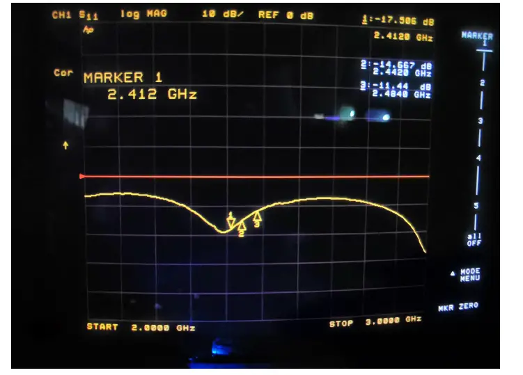
FIG 3

EWN-8822CSS3DA 2.4G Path B

FIG 4 EWN-8822CSS3DA 5G Path A
Module configurations
Module Dimension (L*W*T): 15.2±0.2mm*13.2±0.2mm*2.1±0.2mm。

FIG 6 EWN-8822CSS3DA Module Dimension

Recommended Footprint :

FIG 7 EWN-8822CSS3DA Module Dimension
Pin Definition

See table 7 for the module hardware pin definition.
Table 7 EWN-8822CSS3DA Pin Description
| Pin | Definition | Type | Description | Default Pull | Power level |
| 1 | GND | – | Ground | – | – |
| 2 | Wi-Fi B | I/O | Wi-Fi Path B ANT I/O port | – | – |
| 3 | GND | – | Ground | – | – |
| 4 | GND | – | Ground | – | – |
| 5 | GND | – | Ground | – | – |
| 6 | GND | – | Ground | – | – |
| 7 | GND | – | Ground | – | – |
| 8 | GND | – | Ground | – | – |
| 9 | Wi-Fi A | I/O | Wi-Fi Path A ANT I/O port | – | – |
| 10 | GND | – | Ground | – | – |
| 11 | GND | – | Ground | – | – |
| 12 | BT_ANT | I/O | Bluetooth ANT I/O port | – | – |
| 13 | GND | – | Ground | – | – |
| 14 | G_BT | I/O | GPIO5, General Purpose Input/Output Pin | Internal PD |
VDDIO |
| 15 | WL_DIS_N | I | Reserved | – | VDDIO |
| 16 | WL_WAKE_HOST | O | WLAN to wake-up the host | – | VDDIO |
| 17 | SDIO _CMD | I/O | SDIO interface command line | Internal PU |
VDDIO |
| 18 | SDIO _CLK | I/O | SDIO interface clock line | – | VDDIO |
| 19 | SDIO _DATA_3 | I/O | SDIO interface data line 3 | Internal PU |
VDDIO |
| 20 | SDIO _DATA_2 | I/O | SDIO interface data line 2 | Internal PU |
VDDIO |
| 21 | SDIO _DATA_0 | I/O | SDIO interface data line 0 | Internal PU |
VDDIO |
| 22 | SDIO _DATA_1 | I/O | SDIO interface data line 1 | Internal PU |
VDDIO |
| 23 | GND | – | Ground | – | – |
| 24 | WL_WAKE_HOST | O | WLAN to wake-up the host | – | VDDIO |
| 25 | LTE_COEX1 | I/O | LTE_COEX1, Shared with GPIO6 | – | VDDIO |
| 26 | LTE_COEX2 | I/O | LTE_COEX2, Shared with GPIO12 | – | VDDIO |
| 27 | PCM_SYNC | I/O | PCM SYNC signal | – | VDDIO |
| 28 | PCM_IN | I | PCM data input | – | VDDIO |
| 29 | PCM_OUT | O | PCM data output | – | VDDIO |
| 30 | PCM_CLK | I/O | PCM clock | – | VDDIO |
| 31 | SUSCLK | I/O | External low power clock input (32.768KHz) |
Internal PD |
VDDIO |
| 32 | GND | – | Ground | – | – |
| 33 | LTE_COEX3 | I/O | LTE_COEX3, Shared with GPIO7 | – | VDDIO |
| 34 | VDDIO | I/O | I/O voltage supply input (1.8V typ.) | – | VDDIO |
| 35 | NC | – | No connect | – | – |
| 36 | VDD_3.3V | I/O | Main power voltage source input(3.3V±10%) | – | DC 3.3V±0.3V |
| 37 | NC | – | No connect | – | – |
| 38 | BT_DIS_N | I | Enable pin for Bluetooth device ON: pull high; OFF: pull low External pull low to shut down BT |
Internal PU | VDDIO |
| 39 | GND | – | Ground | – | – |
| 40 | UART_TXD | O | Bluetooth UART interface( connect to host UART RX ) | – | VDDIO |
| 41 | UART_RXD | I | Bluetooth UART interface( connect to host UART TX ) | – | VDDIO |
| 42 | UART_RTS_N | O | Bluetooth UART interface | – | VDDIO |
| 43 | UART_CTS_N | I | Bluetooth UART interface | – | VDDIO |
| 44 | SD_RESET | I | Reset pin for SDIO bus External pull low to reset SDIO bus | Internal PU | VDDIO |
| 45 | G_WL | I/O | GPIO4, General Purpose Input/Output Pin | Internal PD | VDDIO |
| 46 | GND | – | Ground | – | – |
| 47 | NC | – | No connect | – | – |
| 48 | GND | – | Ground | – | – |
| 49 | HOST_WAKE_BT | I | Host wake-up Bluetooth | Internal PD | VDDIO |
| 50 | BT_WAKE_HOST | O | Bluetooth to wake-up the host | Output High | VDDIO |
Note: The internal pull-up/down resistances of the chip are about 50K~100K ohm.
Key material list
Table 8 EWN-8822CSS3DA Key material list
| Type | Model | Footprint | QTY. |
| Diplexers | LD18D2450LAN-D40/M | 1608 | 2PCS |
| RFDIP1607L132A8D1T | |||
| IC | RTL8822CS-VS-CG | QFN76 | 1 PCS |
| Crystal | 40MHz (CX/JWT/TJ) | X3225 | 1 PCS |
Module Photos

Package Information
Carrier dimension: (Unit : mm)


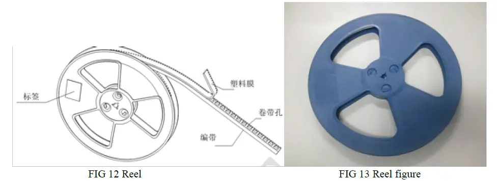
Reel dimension: D=38cm 1400PCS Modules Per Reel
Reference design
Power supply requirement
The module power supply voltage is DC+3.3V, and the maximum module current is 800mA. The power supply design needs to consider the output current and power interference. To avoid the +3.3V power supply from interfering with other circuits on the motherboard, it is recommended to supply to the module using the regulator circuit alone. the recommended DC-DC circuit structure shown in the figure below. A 4.7uF~10uF capacitor is connected in parallel at 3_3VD output to filter out the interference. A bead is connected in series at 3_3VD output. The bead and capacitor must be placed as close to the module as possible. If you need to share +3.3V with other circuits, consider whether the current of the shared power supply is sufficient.

FIG 14 Power supply Circuit schematic
Table 9 DC Characteristics
| Symbol | Parameter | Minimum | Typical | Maximum | Peak Current |
| VDD_3.3V (PIN36) | 3.3V Supply Voltage | 3.0V | 3.3V | 3.6V | 0.8A |
Table 10 Platform Power Rail Requirements
| VDD_3.3V Power range |
VDD_3.3V Ripple |
VDD_3.3V Noise |
Rise time | |
| Min | Max | |||
| +/-0.165V | 300mVpp@switching frequency > 100KHz | 0.5ms | 5ms |
System power on sequrence

Table 11 System Power-On Timing Parameters
| Min. | Typical | Max. | Unit | Description | |
| T18_Ramp/ T33_Ramp | 0.5 | 1.5 | 5 | ms | The 3.3V or 1.8V power ramp up duration. |
| TTrap_Ready | 400 | 500 | – | ms | WLAN eFuse autoload. TTrap_Ready = 500ms (Typical) |
| TSDIO_ Ready | 10 | 20 | 100 | ms | SDIO Not Ready Duration. In this state, the module may respond to commands without the ready bit being set. After the ready bit is set, the host will initiate complete card detection procedure. |
System power off sequrence

Table 12 System Power-Off Timing Parameters
| Min. | Typical | Max. | Unit | Description | |
| TPDN_CHIP | 100 | 100 | – | ms | CHIP_EN keep low duration |
SDIO Interface
The SDIO interface has 4 data lines, a cock signal line and a command signal line. all of the SDIO lines must be equal length. In order to avoid mutual interference, SDIO lines should be avoided to be adjacent and parallel to other data lines, RF lines and power lines, and Surround the data line and clock line with ground copper.
RF circuit
Due to the SMD package, the RF port impedance must be offset after the module is soldered to the motherboard. In order to achieve the best performance,, it is recommended to add a PI-type matching network to the motherboard, as shown below (C11, R21,C6). The value of the PI type matching network needs to be debugged according to the actual motherboard to match RF port impedance to 50 Ohm.

The antenna ANT1 in the figure above must be 50 Ohm. If the antenna is not matched, it is recommended to add a set of PI type matching network at the front of the antenna to match the antenna. Generally, the antenna manufacturers will give Suggestions on matching parameters.

The RF line layout should be matched according to 50ohm. The line impedance is related to the plate, plate thickness, line width and copper spacing. Professional software can be used to calculate the line width. Note: for multilayer plates, the plate thickness should calculate the distance from RF routing layer to GND of the next layer.
There are RF lines Layout principles :
- RF line layout needs to match 50 ohms. The line width can be calculated by professional software. (Note: If it is a multi-layer board, The board thickness should calculate the distance from the RF trace layer to the next ground layer.)
- The RF line must be surrounded by ground copper and ground holes.
- The PI-type matching circuit for adjusting the impedance of the module is placed close to the module. The PI type matching circuit for matching the antenna is placed close to the antenna.


Application Circuit for SD_RESET and BT_DIS_N with Platform
There is internal pull-up, about 100K, resistor design in Module SD_RESET (Pin44) and BT_DIS_N (Pin38) pad. If Host SOC need to control these pins, it is recommended to choose host GPIO without pull capability to avoid voltage divider. Middle range of IO voltage would affect Module booting up (FIG 21).

FIG 21 Host GPIO control WL_REG_ON and BT_REG_ON
If the GPIO connected to SD_RESET and BT_DIS_N by the host has pull-down capability and it can‘t be avoided), suggest to add 10KΩ Pull-Down resistor in circuit to ensure IO is in low level. In this way, Module internal Pull-Up 100KΩ could be neglected (FIG 22). Please note external Pull-Down will cause additional static current. BT_DIS_N exists only high level and low level during power-on. Other uncertain voltage values may cause BT to fail to open.

FIG 22 Add external pull down resistor to ensure low level
PTA interface design reference
EWN-8822CSS3DA supports 3-wire PTA (Packet Traffic Arbitration) interface, and the interface design reference is as follows:
Table 13 Pin Connection Description
| Wi-Fi Module | Other PTA Devices | |
| LTE_COEX1(Pin25) | No Pull | PTA_COEX_BT_STAT |
| LTE_COEX2(Pin26) | No Pull | PTA_COEX_BT_ACT |
| LTE_COEX3(Pin33) | No Pull | PTA_COEX_WL_ACT |
If the surface space is sufficient, it is recommended to reserve series and Pull-Up, Pull-Down resistance for the motherboard.

Motherboard interference avoidance
Motherboard interference comes from: high-speed data interface (HDMI), the Operating frequency of main chip, DDR, DC-DC power supply. The method of avoiding interference according to the characteristics of various signals is also different.
The main methods of interference avoidance include :
- keeping away from the source of interference;
- Adding shields to avoid interference leakage;
- Reasonable layout to eliminate interference.
Interface interference
When HDMI uses the 74.2MHz frequency, its 33x frequency is in the 2.4G band of Wi-Fi, which will seriously interfere with the Wi-Fi signal. If the HDMI frequency is 148.5MHz, although the 16x frequency is not in the Wi-Fi band, the isolation of the frequency is not good, and the Wi-Fi signal will be interfered to some extent. If the distance between the HDMI interface and the Wi-Fi module on the PCB is less than 5cm, the HDMI output display will interfere with the Wi-Fi signal, resulting in problems such as Wi-Fi connection failure and throughput drop.
Therefore, keep the location of the Wi-Fi module away from the HDMI port on the hardware layout to avoid interference. At the same time, if the Wi-Fi antenna is built-in the motherboard, its placement must also be carefully considered to be far from the interface interference. If the antenna is placed in an incorrect position, even if the module is shielded, the interference signal is coupled through the antenna, which will eventually result in a lower Wi-Fi throughput. (Note: In addition to interference, the placement of the internal antenna should also evaluate the effect of the metal interface, motherboard, and housing material on the antenna impedance.)

The main chip interferes with DDR
Because the main chips operate at about 800MHz or DDR2 operate at 667MHz, 3x frequency of 800MHz and 4x frequency of 667MHz are near 2.4GHz band. It must to place Wi-Fi modules and antennas far away from the main chip and DDR. It is strongly recommended that the main chip be isolated from the DDR by a shield. As shown in the figure below.

Recommended secondary reflux temperature curve
The number of reflux shall not exceed 2 times, and the tin feeding height of the half hole of the module shall be no less than 1/4.
The lead-free reflux curve requirements of Wi-Fi module products are shown in FIG 26:


FIG 26 Furnace temperature curve
NOTE:
- The maximum furnace temperature of the module is 260℃, don’t exceed this temperature.
- The gold plating thickness of the module pad is 2u”.
Revision History
| Revision | Release Date | Summary | Revised By |
| V1.0 | 2023-11-09 | First release | Shuize Wang |
| V1.1 | 2023-12-05 | Update module photos | Jisheng Wang |
FCC Statement
This device complies with part 15 of the FCC rules.
Operation is subject to the following two conditions:
- this device may not cause harmful interference, and
- this device must accept any interference received, including interference that may cause undesired operation.
Changes or modifications not expressly approved by the party responsible for compliance could void the user’ s authority to operate the equipment.
NOTE: This equipment has been tested and found to comply with the limits for a Class B digital device, pursuant to part 15 of the FCC Rules. These limits are designed to provide reasonable protection against harmful interference in a residential installation. This equipment generates uses and can radiate radio frequency energy and, if not installed and used in accordance with the instructions, may cause harmful interference to radio communications. However, there is no guarantee that interference will not occur in a particular installation. If this equipment does cause harmful interference to radio or television reception, which can be determined by turning the equipment off and on, the user is encouraged to try to correct the interference by one or more of the following measures:
- Reorient or relocate the receiving antenna.
- Increase the separation between the equipment and receiver.
- Connect the equipment into an outlet on a circuit different from that to which the receiver is connected.
- Consult the dealer or an experienced radio/TV technician for help important announcement
Important Note:
Radiation Exposure Statement
This equipment complies with FCC radiation exposure limits set forth for an uncontrolled environment. This equipment should be installed and operated with minimum distance 20cm between the radiator and your body. This transmitter must not be co-located or operating in conjunction with any other antenna or transmitter. Country Code selection feature to be disabled for products marketed to the US/Canada.
This device is intended only for OEM integrators under the following conditions:
- The antenna must be installed such that 20 cm is maintained between the antenna and users, and
- The transmitter module may not be co-located with any other transmitter or antenna,
- For all products market in US, OEM has to limit the operation channels in CH1 to CH11 for 2.4G band by supplied firmware programming tool. OEM shall not supply any tool or info to the end-user regarding to Regulatory Domain change. (if modular only test Channel 1-11)
As long as the three conditions above are met, further transmitter testing will not be required. However, the OEM integrator is still responsible for testing their end-product for any additional compliance requirements required with this module installed.
Important Note:
In the event that these conditions cannot be met (for example certain laptop configurations or co-location with another transmitter), then the FCC authorization is no longer considered valid and the FCC ID cannot be used on the final product. In these circumstances, the OEM integrator will be responsible for re-evaluating the end product (including the transmitter) and obtaining a separate FCC authorization.
End Product Labeling
The final end product must be labeled in a visible area with the following”
Contains FCC ID: 2AMM6EWN8822CSS3DA ”
Manual Information to the End User
The OEM integrator has to be aware not to provide information to the end user regarding how to install or remove this RF module in the user’s manual of the end product which integrates this module. The end user manual shall include all required regulatory information/warning as show in this manual.
Integration instructions for host product manufacturers according to KDB 996369 D03 OEM
Manual v01r01
List of applicable FCC rules
CFR 47 FCC PART 15 SUBPART C has been investigated. It is applicable to the modular transmitter
Specific operational use conditions
This module is stand-alone modular. If the end product will involve the Multiple simultaneously transmitting condition or different operational conditions for a stand-alone modular transmitter in a host , host manufacturer have to consult with module manufacturer for the installation method in end system.
Limited module procedures
Not applicable
Trace antenna designs
Not applicable
RF exposure considerations
This equipment complies with FCC radiation exposure limits set forth for an uncontrolled environment. This equipment should be installed and operated with minimum distance 20cm between the radiator & your body.
Antennas
This radio transmitter FCC ID: 2AMM6EWN8822CSS3DA has been approved by Federal Communications Commission to operate with the antenna types listed below, with the maximum permissible gain indicated. Antenna types not included in this list that have a gain greater than the maximum gain indicated for any type listed are strictly prohibited for use with this device.
| Antenna No. | Model No. of antenna: | Type of antenna: | Gain of the antenna (Max.) | Frequency range: | |
| Antenna 1 | Antenna 2 | ||||
| Bluetooth | / | PCB Antenna | 5.25 | N/A | 2402-2480MHz |
| 2.4G Wi-Fi | / | PCB Antenna | 3.29 | 3.29 | 2412-2462MHz |
| U-NII-1 | / | PCB Antenna | 4.93 | 4.93 | 5180-5240MHz |
| U-NII-2A | / | PCB Antenna | 5.40 | 5.40 | 5260-5320MHz |
| U-NII-2C | / | PCB Antenna | 5.55 | 5.55 | 5500-5720MHz |
| U-NII-3 | / | PCB Antenna | 5.44 | 5.44 | 5745-5825MHz |
Label and compliance information
The final end product must be labeled in a visible area with the following”
Contains FCC ID: 2AMM6EWN8822CSS3DA “.
Information on test modes and additional testing requirements
Host manufacturer is strongly recommended to confirm compliance with FCC requirements for the transmitter when the module is installed in the host.
Additional testing, Part 15 Subpart B disclaimer
Host manufacturer is responsible for compliance of the host system with module installed with all other applicable requirements for the system such as Part 15 B.
Note EMI Considerations
Host manufacture is recommended to use D04 Module Integration Guide recommending as “best practice” RF design engineering testing and evaluation in case non-linear interactions generate additional non-compliant limits due to module placement to host components or properties.
How to make changes
This module is stand-alone modular. If the end product will involve the Multiple simultaneously transmitting condition or different operational conditions for a stand-alone modular transmitter in a host, host manufacturer have to consult with module manufacturer for the installation method in end system. According to the KDB 996369 D02 Q&A Q12, that a host manufacture only needs to do an evaluation (i.e., no C2PC required when no emission exceeds the limit of any individual device (including unintentional radiators) as a composite. The host manufacturer must fix any failure.
E-mail: sales@eardatek.com
Documents / Resources
 |
EARDATEK EWN-8822CSS3DA WiFi and BT Combo Module [pdf] Instruction Manual EWN8822CSS3DA, 2AMM6EWN8822CSS3DA, EWN-8822CSS3DA WiFi and BT Combo Module, EWN-8822CSS3DA, WiFi and BT Combo Module, BT Combo Module, Module |