ANALOG DEVICES DC3248A Low VIN High Efficiency 10A Step Down DC to DC Module Regulator
USER GUIDE
General Description
The DC3248A evaluation board circuit features the LTM®4659, a high efficiency, 10A step-down power µModule® regulator. The input voltage range is from 2.25V to 5.5V. The output voltage range is 0.5V to VIN. Derating may be necessary for certain VIN, VOUT, frequency and thermal conditions. The DC3248A evaluation board offers the SSTT pin, allowing the user to program output tracking, soft start period and die temperature monitoring.
The MODE/SYNC pin either synchronizes the switching frequency to an external clock, is a clock output, or sets the PWM mode. It can be externally synchronized to a clock from 1MHz to 2.6MHz. The Pulse width modulation (PWM) modes of operation are Forced continuous mode (FCM) for low noise or pulse-skipping mode (PSM) for high efficiency at light load. The LTM4659 defaults to FCM during synchronization and operates in PSM when both the FREQ and MODE/SYNC pins are connected to VIN.
Ordering Information appears at end of demo manual.
The LTM4659 uses external compensation. Users can tune the compensation circuit to ensure the loop is stable and that the desired transient performance can be achieved.
For output loads that demand more than 10A of current, multiple LTM4659s can be paralleled to run out-of-phase to provide more output current without increasing input and output voltage ripples.
The LTM4659 data sheet must be read in conjunction with this evaluation board manual prior to working on or modifying the DC3248A evaluation board.
Features and Benefits
- Tiny surface mount, 4mm × 4mm × 1.43mm LGA
- Silent Switcher®2 architecture
- Ultralow Electromagnetic Interference (EMI) noise
DC3248A Evaluation Board Files
| FILE | DESCRIPTION | ||||||||||||||||||
| DC3248A | Evaluation board circuit design files. | ||||||||||||||||||

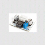
Figure 1. DC3248A Evaluation Board Circuit (Part Marking Is Either Ink Mark or Laser Mark)
Table 1. Performance Summary
Specifications are at TA = 25°C
| PARAMETER | CONDITIONS/NOTES | MIN | TYP | MAX | UNITS | |||||||||||||||||||||||||||||||||||||||
| Input voltage range | 2.25 | 5.5 | V | |||||||||||||||||||||||||||||||||||||||||
| Output voltage | 0.985 | 1.0 | 1.015 | V | ||||||||||||||||||||||||||||||||||||||||
| Maximum continuous output current | Derating is necessary for certain operating conditions. Refer to the data sheet for details. | 10 | ADC | |||||||||||||||||||||||||||||||||||||||||
| Operating frequency | 2 | MHz | ||||||||||||||||||||||||||||||||||||||||||
| Efficiency | VIN = 3.3V, VOUT = 1.0V, IOUT = 10A | 82.16 (see Figure 3) |
% | |||||||||||||||||||||||||||||||||||||||||
| Load transient | VIN = 3.3V, VOUT = 1.0V, ISTEP = 0A to 2.5A | 70 (see Figure 5) |
mV | |||||||||||||||||||||||||||||||||||||||||
Quick Start Required Equipment
- One 0V to 30V DC, 20A power supply
- Electronic load with 20A sink capacity
- Four digital multimeters (DMM)
Procedure
The DC3248A evaluation board is an easy way to evaluate the performance of the LTM4659. See Figure 2 for proper measurement equipment setup and follow the procedure below.
1. Place jumpers in the following positions for a typical application.
| JP1 | RUN | ON | |||||||||||||||||||||
| JP2 | MODE/CLK | CCM | |||||||||||||||||||||
2. With the power off, connect the input power supply, load and meters as shown in Figure 2. Preset the load to 0A and VIN supply to 3.3V.
3. Turn on the power supply at the input. The output voltage should be 1.0V ±1.5% (0.985V to 1.015V).
4. Vary the input voltage from 2.25V to 5.5V and adjust the load current from 0A to 10A. Observe the output voltage regulation, ripple voltage, efficiency, and other parameters.
5. (Optional) To set LTM4659 to PSM, set the MODE/CLK jumper JP8 to PS. See Table 2 for more details.
Table 2. LTM4659 Single-Phase Configuration
| FREQ PIN CONNECTION | MODE/SYNC PIN CONNECTION | MODE OF OPERATION | SWITCHING FREQUENCY | |||||||||||||||||||||||||||||||||||||||||
| VIN | Clock input | FCM | External clock | |||||||||||||||||||||||||||||||||||||||||
| VIN | AGND | FCM | 2MHz default | |||||||||||||||||||||||||||||||||||||||||
| VIN | VIN | PSM | 2MHz default | |||||||||||||||||||||||||||||||||||||||||
| Resistor to AGND | Clock output | FCM | RFREQ-programmed | |||||||||||||||||||||||||||||||||||||||||
6. (Optional) For the optional load transient test, apply an adjustable pulse signal between IOSTEP_CLK and GND test points. The pulse amplitude sets the load step current amplitude. Keep the pulse width short (<1ms) and pulse duty cycle low (<5%) to limit the thermal stress on the load transient circuit.
7. (Optional) LTM4659 can be synchronized to an external clock signal. Place the JP8 jumper on CLK and apply a clock signal on the CLK test point.
8. (Optional) The output of LTM4659 can track another voltage. This external voltage can be connected to the test point TRACK on this board.

Typical Performance Characteristics

Figure 7. Thermal Image of LTM4659 at VIN = 3.3V, VOUT = 1.0V, IOUT = 10A (TA = 25°C, No Forced Airflow)
DC3248A Bill of Materials
| ITEM | QTY | REFERENCE | PART DESCRIPTION | MANUFACTURER/PART NUMBER | ||||||||||||||||||||||||||||||||||||||||
| Required Circuit Components | ||||||||||||||||||||||||||||||||||||||||||||
| 1 | 4 | C1, C3, CIN1, CIN5 | CAP., 10μF, X7R, 16V, 10%, 0805 | TAIYO YUDEN, EMK212BB7106MG-T | ||||||||||||||||||||||||||||||||||||||||
| 2 | 2 | C2, CIN6 | CAP., 150μF, ALUM ELECT, 10V, 20%, 8mm × 6.9mm |
PANASONIC, 10SVP150MX | ||||||||||||||||||||||||||||||||||||||||
| 3 | 1 | C4 | CAP., 0.1μF, X7R, 6.3V, 10%, 0603 | AVX, 06036C104KAT2A | ||||||||||||||||||||||||||||||||||||||||
| 4 | 1 | C13 | CAP., 680pF, C0G, 25V, 5%, 0603 | AVX, 06033A681JAT2A | ||||||||||||||||||||||||||||||||||||||||
| 5 | 1 | CIN2 | CAP., 22μF, X5R, 10V, 20%, 0603 | AVX, 0603ZD226MAT2A | ||||||||||||||||||||||||||||||||||||||||
| 6 | 2 | CIN3, CIN4 | CAP., 22μF, X5R, 16V, 10%, 0805 | TDK, C2012X5R1C226M125AC | ||||||||||||||||||||||||||||||||||||||||
| 7 | 1 | COUT1 | CAP., 22μF, X5R, 6.3V, 20%, 0603 | MURATA, GRM188R60J226MEA0D | ||||||||||||||||||||||||||||||||||||||||
| 8 | 1 | COUT2 | CAP., 22μF, X5R, 6.3V, 20%, 0805 | MURATA, C0805C226M9PACTU | ||||||||||||||||||||||||||||||||||||||||
| 9 | 1 | COUT3 | CAP., 100μF, X5R, 6.3V, 20%, 0805 | MURATA, GRM21BR60J107ME15K | ||||||||||||||||||||||||||||||||||||||||
| 10 | 1 | R3 | RES., 100kΩ, 1%, 1/10W, 0603 | STACKPOLE ELECTRONICS, INC., RMCF0603FG100K | ||||||||||||||||||||||||||||||||||||||||
| 11 | 2 | R4, R6 | RES., 60.4kΩ, 1%, 1/10W, 0603, AEC-Q200 | VISHAY, CRCW060360K4FKEA | ||||||||||||||||||||||||||||||||||||||||
| 12 | 1 | R15 | RES., 6.8 kΩ, 5%, 1/16W, 0603 | KOA SPEER, RK73B1JTTD682J | ||||||||||||||||||||||||||||||||||||||||
| 13 | 1 | U1 | IC, 5.5VIN, 10A μModule, 4mm × 4mm PCKG, BGA | ADI, LTM4659EV#PBF | ||||||||||||||||||||||||||||||||||||||||
| Additional Evaluation Board Circuit Components | ||||||||||||||||||||||||||||||||||||||||||||
| 1 | 0 | C5–C7, C12 | CAP., OPTION, 0603 | |||||||||||||||||||||||||||||||||||||||||
| 2 | 0 | C11 | CAP., OPTION, 0805 | |||||||||||||||||||||||||||||||||||||||||
| 3 | 1 | R11 | RES., 0Ω, 1/10W, 0603 | BOURNS, CR0603-J/-000ELF | ||||||||||||||||||||||||||||||||||||||||
| 4 | 0 | R12 | RES., OPTION, 0603 | |||||||||||||||||||||||||||||||||||||||||
| 5 | 3 | C8–C10 | CAP., 1μF, X7R, 16V, 10%, 0603 | KEMET, C0603C105K4RAC7867 | ||||||||||||||||||||||||||||||||||||||||
| 6 | 1 | L1 | IND., 100 AT 100MHz, FERRITE BEAD, 25%, 8A, 6m, 1812 |
WURTH ELEKTRONIK, 74279226101 | ||||||||||||||||||||||||||||||||||||||||
| 7 | 1 | Q1 | XSTR., MOSFET, N-CHAN, 30V, 5.5A, 3-PIN SOT-23 |
VISHAY, Si2338DS-T1-GE3 | ||||||||||||||||||||||||||||||||||||||||
| 8 | 1 | R13 | RES., 10kΩ, 1%, 1/10W, 0603, AEC-Q200 | VISHAY, CRCW060310K0FKEA | ||||||||||||||||||||||||||||||||||||||||
| 9 | 1 | R14 | RES., 10Ω, 1%, 1/10W, 0603 | VISHAY, CRCW060310R0FKEA | ||||||||||||||||||||||||||||||||||||||||
| 10 | 1 | RS1 | RES., 0.020Ω, 1%, 1W, 1206, PWR, METAL, SENSE, AEC-Q200 | VISHAY, WSLP1206R0200FEA | ||||||||||||||||||||||||||||||||||||||||
| Hardware: For Evaluation Board Circuit Only | ||||||||||||||||||||||||||||||||||||||||||||
| 1 | 8 | E1-E8 | TEST POINT, TURRET, 0.094˝ MTG. HOLE, PCB 0.062˝ THK |
MILL-MAX, 2501-2-00-80-00-00-07-0 | ||||||||||||||||||||||||||||||||||||||||
| 2 | 5 | J1–J5 | CONN., BANANA JACK, FEMALE, THT, NON- INSULATED, SWAGE, 0.218˝ |
KEYSTONE, 575-4 | ||||||||||||||||||||||||||||||||||||||||
| 3 | 2 | J6, J7 | CONN., RF, BNC, RCPT, JACK, 5-PIN, ST, THT, 50 | AMPHENOL RF, 112404 | ||||||||||||||||||||||||||||||||||||||||
| 4 | 1 | JP1 | CONN., HDR, MALE, 1 × 3, 2mm, VERT, ST, THT, NO SUBS. ALLOWED | WURTH ELEKTRONIK, 62000311121 | ||||||||||||||||||||||||||||||||||||||||
| 5 | 1 | JP8 | CONN., HDR., MALE, 2 × 3, 2mm, VERT, ST, THT | WURTH ELEKTRONIK, 62000621121 | ||||||||||||||||||||||||||||||||||||||||
| 6 | 4 | MP1–MP4 | STANDOFF, NYLON, SNAP-ON, 0.50˝ | KEYSTONE, 8833 | ||||||||||||||||||||||||||||||||||||||||
| 7 | 2 | XJP1, XJP8 | CONN., SHUNT, FEMALE, 2-POS, 2mm | WURTH ELEKTRONIK, 60800213421 | ||||||||||||||||||||||||||||||||||||||||
DC3248A Schematic

Ordering Information
| REVISION NUMBER | REVISION DATE | DESCRIPTION | PAGES CHANGED | |||||||||||||||||||||||||||||||||||||||||
| 0 | 04/24 | Initial release | — | |||||||||||||||||||||||||||||||||||||||||
ASSUMED BY ANALOG DEVICES FOR ITS USE, NOR FOR ANY INFRINGEMENTS OF PATENTS OR OTHER RIGHTS OF THIRD PARTIES THAT MAY RESULT FROM ITS USE. SPECIFICATIONS ARE SUBJECT TO CHANGE WITHOUT NOTICE. NO LICENCE, EITHER EXPRESSED OR IMPLIED, IS GRANTED UNDER ANY ADI PATENT RIGHT, COPYRIGHT, MASK WORK RIGHT, OR ANY OTHER ADI INTELLECTUAL PROPERTY RIGHT RELATING TO ANY COMBINATION, MACHINE, OR PROCESS WHICH ADI PRODUCTS ALL INFORMATION CONTAINED HEREIN IS PROVIDED “AS IS” WITHOUT REPRESENTATION OR WARRANTY. NO RESPONSIBILITY IS OR SERVICES ARE USED. TRADEMARKS AND REGISTERED TRADEMARKS ARE THE PROPERTY OF THEIR RESPECTIVE OWNERS.
Documents / Resources
 |
ANALOG DEVICES DC3248A Low VIN High Efficiency 10A Step Down DC to DC Module Regulator [pdf] User Guide DC3248A Low VIN High Efficiency 10A Step Down DC to DC Module Regulator, DC3248A, Low VIN High Efficiency 10A Step Down DC to DC Module Regulator, High Efficiency 10A Step Down DC to DC Module Regulator, 10A Step Down DC to DC Module Regulator, Step Down DC to DC Module Regulator, DC to DC Module Regulator, Module Regulator, Regulator |