![]() User Guide | EVAL-AD7173-8ARDZ
User Guide | EVAL-AD7173-8ARDZ
UG-2322
Evaluating the AD7173-8 24-Bit, 8-/16-Channel, 31.25kSPS, Sigma-Delta ADC with True Rail-to-Rail Buffers
FEATURES
► Full featured evaluation board for the AD7173-8
► PC control in conjunction with the Analog Devices, Inc., SDP-K1 board (EVAL-SDP-CK1Z)
► PC software for control and data analysis (time domain)
► Standalone capability
DOCUMENTS NEEDED
► AD7173-8 data sheet
REQUIRED SOFTWARE
► ACE software (see the Installation Guide section)
EQUIPMENT NEEDED
► EVAL-AD7173-8ARDZ
► EVAL-SDP-CK1Z
► DC signal source
► USB cable
► PC running Windows with USB 2.0 port
ONLINE RESOURCES
► Schematic, PCB layout, and bill of materials
EVALUATION BOARD

GENERAL DESCRIPTION
The EVAL-AD7173-8ARDZ evaluation board features the AD7173-8, a 24-bit, 250kSPS analog-to-digital converter (ADC) with integrated analog input buffers, on-board power supply regulation, and an external amplifier section for amplifier evaluation. A 5V USB is regulated to 5V and 3.3V; this supplies the AD7173-8 and support components. The evaluation board connects to a USB port via the system demonstration platform (SDP) controller board EVAL-SDP-CK1Z (SDP-K1).
The AD717x ACE software fully configures the AD7173-8 device functionality via a user accessible register interface and provides DC time domain analysis in the form of waveform graphs, histograms, and associated noise analysis for ADC performance evaluation.
Full specifications on the AD7173-8 are available in the product data sheet, which must be consulted in conjunction with this user guide when working with the evaluation board. Full details for the SDP-K1 controller board are available on the Analog Devices website.
PLEASE SEE THE LAST PAGE FOR AN IMPORTANT WARNING AND LEGAL TERMS AND CONDITIONS.
REVISION HISTORY
4/2025—Revision A: Initial Version
EVALUATION BOARD BLOCK DIAGRAM

QUICK START GUIDE
RECOMMENDED QUICK START GUIDE
Use the following procedure to set up the evaluation board:
- With the SDP-K1 board disconnected from the USB port of the PC, install the ACE software (can be downloaded online).
Restart the PC after the software installation is complete (for complete software installation instructions, see the Installing the ACE Software section). - Connect the SDP-K1 board to the EVAL-AD7173-8ARDZ board via Arduino connector.
- Connect the SDP-K1 board to the PC via the USB cable. For Windows® XP, it may be necessary to search for the SDP drivers. Choose to automatically search for the drivers for the SDP board if prompted by the operating system.
- Launch the ACE software.
 QUICK START MEASUREMENT
Use the following procedure to capture data quickly:
- Connect the DC signal source to the selected voltage input (for example, AIN0 and AIN1 for differential input).
- Launch the ACE software and select the AD7173-8 Board (see Figure 5).
- Double click the AD7173-8 chip then click the Proceed to Analysis (see Figure 5).
- In the Waveform tab, the user can capture and measure the data by clicking Run Once (Label 14, Figure 13).
The Sample Count in the top left area of the Waveform tab (Label 12, Figure 13) sets the number of samples collected in each batch.
HARDWARE GUIDE
DEVICE DESCRIPTION
The AD7173-8 is a highly accurate, high resolution, multiplexed, 8-/16-channel (full/pseudo-differential) Σ-Δ ADC. The AD7173-8 has a maximum channel-to-channel scan rate of 6.21kSPS (161µs) for fully settled data. The output data rates range from 1.25SPS
to 31.25kSPS. The device includes integrated analog input and reference buffers, an integrated precision 2.5V reference, and an integrated oscillator.
SETUP PROCEDURES
After following the instructions in the Installing the ACE Software section, set up the evaluation board and the SDP-K1 board as detailed in this section.
The ACE software and AD717x board plug-in must be installed before connecting the EVAL-AD7173-8ARDZ and the EVAL-SDP-CK1Z board to the USB port of the PC to ensure that the PC recognizes the evaluation system.
Configuring the Evaluation and SDP Boards
Use the following procedure to configure the boards:
- Connect the SDP-K1 to the Arduino headers of the evaluation board.
- Connect the SDP board to the PC using the USB cable.
HARDWARE LINK OPTIONS
See Table 1 for all the EVAL-AD7173-8ARDZ link options.
| Link Number | Default Position | Description |
| LK1 | B | Selects the voltage applied to the AVDD1 pin. Operates using the AVDD +5V supply (default). When inserted in Position A, sets the AVDD1 voltage to the +3.3V supply from the ADP150 (U6) regulator. Setting AVDD1 = +3.3V is not allowed when AVSS =−2.5V. |
| LK2 | B | Selects the voltage applied to the AVDD2 pin. Operates using the AVDD +5V supply (default). When inserted in Position A, sets the AVDD2 voltage to the +3.3V supply from the ADP150 (U6) regulator. Setting AVDD2 = +3.3V is not allowed when AVSS =−2.5V. |
| LK3 | B | Selects the external clock input or internal clock output (default). When inserted in Position A, selects the CRYSTAL OPTION (Y1). |
| LK4 | Inserted | Insert to connect REF− to AVSS. |
| LK5 | B | Connects REF+ to 5V external reference (default). When inserted in Position A, REF+ is connected to 2.5V internal reference. |
| LK6 | A | Turns on the LTC3129 (U3) to supply 7V to the low-dropout (LDO) linear regulators (default). When inserted in Position B, turns off the LTC3129 (U3). |
| LK7 | B | Shifts the voltage of AVDD 5.5V to 7V when inserted in Position A. When inserted in Position B, AVDD 5.5V is set to 5.5V (default). |
| LK8 | A | Turns on the ADP7118 (U10) to supply for AVDD 5.5V. The AVDD 5.5V is supplied with 5.5V from ADP7118 regulator (default). When inserted in Position B, turns off the ADP7118 (U10). |
| LK9 | A | Turns on the 5V LDO to supply for AVDD 5V. The AVDD 5V is supplied with 5V from ADP7118 (U11) regulator (default). When inserted in Position B, turns off the ADP7118 (U11). |
| LK10 | A | Turns on the 2.5V LDO to supply for AVDD 2.5V. The AVDD 2.5V is supplied with 2.5V from LT1962 (U4) regulator (default). When inserted in Position B, turns off the LT1962 (U4). |
| LK11 | A | Turns on the LTC1983 (U2) to supply for the ADP7182 (U5) 2.5V linear regulator (default). When inserted in Position B, turns off the LTC1983 (U2). |
| LK12 | A | Turns on the ADP7182 (U5) to supply for −2.5V. The −2.5V is supplied with −2.5V from the ADP7182 regulator (default); AVSS can be connected to ground depending on S1. When inserted in Position B, turns off the ADP7182 (U5). |
| LK13 | A | Turns on the 3.3V LDO to supply for IOVDD 3.3V. The IOVDD 3.3V is supplied with 3.3V from ADP150 (U6) regulator (default). When inserted in Position B, turns off the ADP150 (U6). |
| LK14 | Removed | Insert LK14 when performing NOISE TEST. |
| LK15 | A | Set to A, connects AIN0 to ADC Driver. Set to B, connects/directs AIN0 to ADC (default). Remove LK16 when connecting AIN0 to surfboard. |
| LK16 | B | Set to A, connects AIN0 to ADC Driver. Set to B, connects/directs AIN0 to ADC (default). Remove LK16 when connecting AIN0to surfboard. |
| LK17 | B | Set to A, connects AIN1 to ADC Driver. Set to B, connects/directs AIN1 to ADC (default). Remove LK17 when connecting AIN0 to surfboard. |
| LK18 | A | Set to A, connects −VS to GND (default). Set to B, connects −VS to −2.5 V. Remove LK18 when using external supply. |
| LK19 | B | Set to A, connects +VS to AVDD 5 V. Set to B, connects +VS to AVDD 5.5 V (default). Remove LK19 when using external supply. |
| LK20 | Inserted | When inserted, initiates power down for the ADA4945-1/ADA4940-1. Remove when using the ADC DRIVER. Insert LK20 when performing NOISE TEST or when Surfboard is connected. |
| LK21 | A | Set to A, connects SCLK to standard Arduino connection (default). Set to B when using multiple boards; connects SCLK to alternative Arduino connection. |
| LK22 | A | Set to A, connects DOUT to standard Arduino connection (default). Set to B when using multiple boards; connects DOUT to alternative Arduino connection. |
| LK23 | A | Set to A, connects DIN to standard Arduino connection (default). Set to B when using multiple boards; connects DIN to alternative Arduino connection. |
| LK24 | A | Set to A, connects CS to standard Arduino connection (default). Otherwise, select different CS for stacking multiple boards. |
ON-BOARD CONNECTIONS
Table 2. On-Board Connections
| Connector | Function | Connector Type |
| J1 | External clock input or ADC internal clock output | SubMiniature version B (SMB) connector jack, male Pin 50Ω through hole solder |
| J2 | External bench top voltage supply option for AVDD +5V, AVDD +2.5V, AVSS −2.5V, and IOVDD inputs on the AD7173-8 | Screw terminal block, 2.54mm pitch |
| J4 | Arduino headers (power) | 8 position receptacle connector, 2.54mm pitch |
| J5 | Arduino header (Digital 1) | 10 position receptacle connector, 2.54mm pitch |
| J6 | Arduino header (analog) | 6 position receptacle connector, 2.54mm pitch |
| J7 | Arduino header (Digital 0) | 8 position receptacle connector, 2.54mm pitch |
| J8 | Peripheral module (PMOD) form factor | 12-pin header, 2.54mm pitch |
| J9 | Arduino header lead frame chip scale package (LFCSP) | 6 position, 2 row, receptacle connector, 2.54mm pitch |
| J15 and J17 | Analog input terminal block; wired connection to external source or sensor | Power socket block, 8-pin, 2.54mm pitch, 3.5mm solder tail |
| J16 | Analog input terminal block; wired connection to external source or sensor | Power socket block, 6-pin, 2.54mm pitch, 3.5mm solder tail |
| J18 | General‐purpose input/output (GPIO) terminal | 4 position ,1 row vertical printed circuit board (PCB) header, 2.54mm pitch |
| J19 | Surfboard header (optional) | 7-way, 2.54 mm pin socket |
| J20 | Surfboard header (optional) | 7-way, 2.54 mm pin header |
POWER SUPPLIES
The evaluation board receives power through the controller board when connected to the PC via 5V USB. Linear regulators generate the required power supply levels from the applied USB voltage.
Each regulator can be shut down using their shut down links (see Table 3).
To configure the on-board power supplies, refer to the following descriptions:
► AVDD1 and AVSS selection (S1)
► 5V supply (default)
► Position switch (S1) to SINGLE on the board
► 5V regulator supplies AVDD1
► AVSS tied to AGND
► 2.5V split supply
► Position switch (S1) to SPLIT on the board
► 2.5V regulator supplies AVDD1
► −3V regulator and −2.5V regulator supplies AVSS
► AVDD1 and AVDD2 selection (LK1 and LK2)
► 5V supply (default)
► Set LK1 and/or LK2 to Position B
► 5V regulator supplies AVDD1
► 3.3V supply
► Set LK1 and/or LK2 to Position A
► 3.3V regulator supplies IOVDD
► External AVDD/AVSS
► Set LK1, LK2, LK9, LK10, LK11, LK12, and LKL13 to Position B
► When using external AVDD only, set S1 to SINGLE, and connect external AVDD Pin 1 of J2.
► When using external AVDD and AVSS, set S1 to SPLIT, and connect external AVDD and AVSS to Pin 2 and Pin 3 of J2, respectively.
Table 3. Power Supplies Link Options
| Supply | Regulator | Shut Down Link |
| +5V Regulator | ADP7118ACPZN5.0-R7 | LK9 |
| +2.5V Regulator | LT1962EMS8-2.5#PBF | LK10 |
| −2.5V Regulator | ADP7182AUJZ-2.5-R7 | LK12 |
| +3.3V Regulator | ADP150ACBZ-3.3-R7 | LK13 |
SERIAL INTERFACE
There are four primary signals: CS, SCLK, MOSI/DIN, and MISO/DOUT (all are inputs, except for MISO/DOUT, which is an output). The EVAL-AD7173-8ARDZ evaluation board connects to any microcontroller board that uses the Arduino standard headers.
This can be developed in user code for a variety of platforms.
Serial communication options:
► Arduino connection using the SDP-K1
► PMOD connector
► Standalone mode
Note: the links LK21, LK22, LK23, and LK24 through J5 provide access to all serial peripheral interface (SPI) signals and set the input/output voltage levels.
For an introduction to the SPI, see Introduction to SPI Interface.
 ANALOG INPUTS
The EVAL-AD7173-8ARDZ primary analog inputs can be applied on J15, J16, and J17 which are at the left side of the board (see Figure 1). Differential analog inputs are applied on AIN0 and AIN1 when using the ADC driver (when using ADC driver, enable AIN+/AINbuffers).
The AD7173-8 evaluation software is set up to analyze DC inputs to the ADC. The AD7173-8 input buffers work for DC input signals.
REFERENCE OPTIONS
The on-board EVAL-AD7173-8ARDZ link configuration offers the following reference options:
► The AD7173-8 internal 2.5V reference
► The default ADR4550 on-board external reference
► External reference connector J17 through the AIN1/REF2+ and AIN0/REF2− pins
SELECTING THE REFERENCE SOURCE
Software
The following steps show the setting reference for Channel 0. For channel n, go to register SETUPCON[n].
- Board must be connected to ACE.
- Open the AD7173-8 memory map (Memory Map Side-BySide).
- Search for the SETUPCON[0] register.
- Set REF_SEL_N[0] to the desired reference source or the Data (Hex) to the relevant bits.
a. External Reference 1 − REF+/− (Hex Value 00, Binary Value 00).
b. External Reference 2 − REF2+/− (Hex Value 01, Binary Value 01).
c. Internal 2.5V Reference REFOUT, AVSS (Hex Value 02, Binary Value 10).
d. AVDD1 − AVSS (Hex Value 03, Binary Value 11).
 Hardware
Table 4. Reference Link Options
| Link Numbers | Type | Default Position | Description |
| LK4 | Link | Inserted | Inserted: connects REF− to AVSS. Removed: disconnects REF− to AVSS. |
| LK5 | Link | B | REF+/− connections. Set to A: connects REF+ to REFOUT. Set to B: connects REF+ to on board the ADR4550 external reference. |
SOFTWARE GUIDE
ACE SOFTWARE
The ACE software is available at the Analog Devices website.
See the Quick Start Guide section or for the step by step installation, see the Installation Guide section.
INSTALLATION GUIDE
The EVAL-AD7173-8ARDZ evaluation kit includes a link to the software that needs to be installed before using the EVALAD7173-8ARDZ evaluation board.
Warning: the ACE software and board plug-in must be installed before connecting both the evaluation board and the SDP-K1 board to the PC. This ensures that the evaluations system is recognized when it is connected to the PC.
Installing the ACE Software
To install the ACE software, follow these steps:
- With the SDP board disconnected from the USB port of the PC, download the ACE software package to start the ACE software installation.
- Click Download ACE Installer.
- Run the installer and follow the instructions to complete the software installation process.
During the installation process, ensure to select Precision Converter Components () when prompted and enable the LibIIO Wrapper () to ensure that all necessary software components are installed (see Figure 6). The LibIIO Wrapper must be installed for ACE to detect the connected hardware. If you need to install the LibIIO Wrapper after ACE has been installed, click the Help button in the main ACE window. In the ACE Help panel that appears, expand the Application Resources section, and there is a link to run a local copy of the IIO prerequisite software components (IIO Components Installer (Local copy)). See Figure 7 and Figure 8.
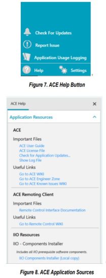 When prompted to select LibIIO components, ensure to select LibIIO and LibIIODrivers options, then click Install (see Figure 9).
Evaluation Hardware Setup
When the ACE software installation is complete, take the following steps to set up the SDP-K1 and evaluation board together:
- Connect the SDP-K1 and evaluation board using the Arduino headers.
- Connect the power supplies configuration.
- Connect the USB cable to the SDP-K1.
- Open the ACE software.
Software Operation
To start the ACE software, from the Windows Start menu, click Analog Devices > ACE. The software window opens (see Figure 10) until the software recognizes the AD7173-8 evaluation board.
When the software recognizes the board, double click on the icon in the Start view to open the main window as shown in Figure 11.
Ensure that you already have the AD717x-8 board plug-in in the plug-in manager.
By clicking on the part in the main ACE software window (see Figure 11), the AD7173-8 chip view opens (Figure 12).
The chip view shows the block diagram of the AD7173-8. This tab allows the user to select inputs, set up the ADC, reset the ADC, and view errors present, as well as configure the device for different demonstration modes. Figure 12 shows the chip view in detail, and the following sections discuss the different elements on the chip view of the software window.
 Quick Configuration Tab
The QUICK CONFIGURATION tab shows a block diagram of the AD7173-8. This tab allows the user to select inputs, set up the ADC, reset the ADC, and view errors present, as well as configure the device.
The ACE software features a quick configuration tab to configure the AD7173-8 through the following:
► Functional block diagram: the functional block diagram of the AD7173-8 (Label 1 in Figure 12) shows each of the functional blocks within the AD7173-8. Click a functional block on this diagram to open the configuration pop-up window for that block.
► Configuration pop-up button: each block has a pop-up window (Label 2 in Figure 12) which opens a different window to configure the relevant block.
► External parameters: the following are the four external parameters that are set by the EVAL-AD7173-8ARDZ but must be entered into the software:
► AVDD1 and AVDD2 (Label 3 in Figure 12)
► Ext. REF− and Ext. REF+ (Label 4 in Figure 12)
► IOVDD (Label 5 in Figure 12)
► AVSS (Label 6 in Figure 12)
The external reference on the EVAL-AD7173-8ARDZ is set to 2.5V by using the ADR4525. If bypassing the ADR4525 on the board, change the external reference voltage value in the software to ensure correct calculation of results in the Waveform and Histogram tabs in the waveform analysis window.
► Status bar: the status bar (Label 7 in Figure 12) displays status updates.
► Memory map button: opens the Memory Map tab.
► Waveform analysis button: opens the Waveform tab.
 Waveform Tab
The Waveform tab can display the different waveforms for voltage input, current input and select the channel. The waveform tab graphs the conversions gathered and processes the data, calculating the peak-to-peak noise, RMS noise, and resolution.
The ACE software features different configuration settings to display results through the following:
► Waveform graph and controls: the data waveform graph (Label 10 in Figure 13) shows each successive sample of the ADC output. Zoom in on the data in the graph using the control toolbar (Label 11 in Figure 13). Change the scales on the graph by typing values into the x-axis and y-axis fields.
► Samples: the samples numeric control (Label 12 in Figure 13) sets the number of samples gathered per batch.
► Serial interface and internal reference: sets the ADC mode, enables DATA_STAT and internal reference (Label 13 in Figure 13).
► Run: click Run Once or Run Continuously (Label 14 in Figure 13) to start gathering ADC results. If Run Once is clicked, the ADC returns the number of samples specified by the samples control. If Run Continuously, the ADC continuously returns samples until stopped by the user. Samples specify the amounts of samples to be shown on the data graph. This control is unrelated to the ADC mode. Results appear in the waveform graph (Label 10 in Figure 13).
► Channel selection: the channel selection control (Label 15 in Figure 13) selects which channel is displayed on the data waveform. These controls only affect the waveform graphs and have no effect on the channel settings in the ADC register map.
► Display units and axis controls: click the units dropdown box (Label 16 in Figure 13) to select whether the data graph displays in units of voltages/amps or codes. This control is independent for each graph.
► Results pane: the RESULTS pane (Label 17 in Figure 13) displays parametric values for the selected display format. The bottom of the RESULTS pane also has buttons that allow the user to import or export sample data.
 Histogram Tab
The Histogram tab generates a histogram using the gathered samples and processes the data, calculating the peak-to-peak noise, RMS noise, and resolution. The ACE software features a histogram tab that can be configured through the following:
► Histogram graph and controls: the data histogram graph (Label 18 in Figure 14) shows the number of times each sample of the ADC output occurs. Zoom in on the data using the control toolbar (Label 19 in Figure 14) in the graph.
► Channel selection: the channel selection control (Label 20 in Figure 14) selects which channel is displayed on the data waveform.
These controls only affect the waveform graphs and have no effect on the channel settings in the ADC register map.
► Display units and axis controls: click the units dropdown box (Label 21 in Figure 14) to select whether the data graph displays in units of voltages/amps or codes. This control is independent for each graph.
 Memory Map
The ACE software features a memory map as an additional method to configure the AD7173-8 through the following:
► Register tree: the register maps nested list (Label 22 in Figure 15) shows the full register map in a tree control. Each register is shown. Click the expand button next to each register to show all the bit fields contained within that register.
► Register tree search: the register tree search box (Label 23 in Figure 15) allows the user to search the tree for any register or bit field. Enter a value into this field to filter the register tree.
► Register and bit field control: the register and bit field control section (Label 24 in Figure 15) allows the user to change the individual bit of the register selected in the register tree by clicking the bits or by programming the register value directly into the number control field (Label 25 in Figure 15). This control also shows all bit fields for the selected register. Change the values by using a dropdown box (Label 26 in Figure 15) or by selecting or clearing a checkbox (Label 27 in Figure 15).
► Documentation: the bit field documentation (Label 28 in Figure 15) contains the documentation for the register or the bit field selected. This field can be updated by selecting a register or bit field in the register tree or hovering over the register or bit field in the register tree or register control. This documentation is displayed by clicking the button labeled 28 in Figure 15.
► Import and export: save and load (Label 29 in Figure 15) allow the user to save the current register map setting to a file and to load the setting from the same file, respectively.

![]() ESD Caution
ESD Caution
ESD (electrostatic discharge) sensitive device. Charged devices and circuit boards can discharge without detection. Although this product features patented or proprietary protection circuitry, damage may occur on devices subjected to high energy ESD. Therefore, proper ESD precautions should be taken to avoid performance degradation or loss of functionality.
Legal Terms and Conditions
By using the evaluation board discussed herein (together with any tools, components documentation or support materials, the “Evaluation Board”), you are agreeing to be bound by the terms and conditions set forth below (“Agreement”) unless you have purchased the Evaluation Board, in which case the Analog Devices Standard Terms and Conditions of Sale shall govern. Do not use the Evaluation Board until you have read and agreed to the Agreement. Your use of the Evaluation Board shall signify your acceptance of the Agreement. This Agreement is made by and between you (“Customer”) and Analog Devices, Inc. (“ADI”), with its principal place of business at Subject to the terms and conditions of the Agreement, ADI hereby grants to Customer a free, limited, personal, temporary, non-exclusive, non-sublicensable, non-transferable license to use the Evaluation Board FOR EVALUATION PURPOSES ONLY. Customer understands and agrees that the Evaluation Board is provided for the sole and exclusive purpose referenced above, and agrees not to use the Evaluation Board for any other purpose. Furthermore, the license granted is expressly made subject to the following additional limitations: Customer shall not (i) rent, lease, display, sell, transfer, assign, sublicense, or distribute the Evaluation Board; and (ii) permit any Third Party to access the Evaluation Board. As used herein, the term “Third Party” includes any entity other than ADI, Customer, their employees, affiliates and in-house consultants. The Evaluation Board is NOT sold to Customer; all rights not expressly granted herein, including ownership of the Evaluation Board, are reserved by ADI. CONFIDENTIALITY. This Agreement and the Evaluation Board shall all be considered the confidential and proprietary information of ADI. Customer may not disclose or transfer any portion of the Evaluation Board to any other party for any reason. Upon discontinuation of use of the Evaluation Board or termination of this Agreement, Customer agrees to promptly return the Evaluation Board to ADI. ADDITIONAL RESTRICTIONS. Customer may not disassemble, decompile or reverse engineer chips on the Evaluation Board. Customer shall inform ADI of any occurred damages or any modifications or alterations it makes to the Evaluation Board, including but not limited to soldering or any other activity that affects the material content of the Evaluation Board. Modifications to the Evaluation Board must comply with applicable law, including but not limited to the RoHS Directive. TERMINATION. ADI may terminate this Agreement at any time upon giving written notice to Customer. Customer agrees to return to ADI the Evaluation Board at that time. LIMITATION OF LIABILITY. THE EVALUATION BOARD PROVIDED HEREUNDER IS PROVIDED “AS IS” AND ADI MAKES NO WARRANTIES OR REPRESENTATIONS OF ANY KIND WITH RESPECT TO IT. ADI SPECIFICALLY DISCLAIMS ANY REPRESENTATIONS, ENDORSEMENTS, GUARANTEES, OR WARRANTIES, EXPRESS OR IMPLIED, RELATED TO THE EVALUATION BOARD INCLUDING, BUT NOT LIMITED TO, THE IMPLIED WARRANTY OF MERCHANTABILITY, TITLE, FITNESS FOR A PARTICULAR PURPOSE OR NONINFRINGEMENT OF INTELLECTUAL PROPERTY RIGHTS. IN NO EVENT WILL ADI AND ITS LICENSORS BE LIABLE FOR ANY INCIDENTAL, SPECIAL, INDIRECT, OR CONSEQUENTIAL DAMAGES RESULTING FROM CUSTOMER’S POSSESSION OR USE OF THE EVALUATION BOARD, INCLUDING BUT NOT LIMITED TO LOST PROFITS, DELAY COSTS, LABOR COSTS OR LOSS OF GOODWILL. ADI’S TOTAL LIABILITY FROM ANY AND ALL CAUSES SHALL BE LIMITED TO THE AMOUNT OF ONE HUNDRED US DOLLARS ($100.00). EXPORT. Customer agrees that it will not directly or indirectly export the Evaluation Board to another country, and that it will comply with all applicable United States federal laws and regulations relating to exports. GOVERNING LAW. This Agreement shall be governed by and construed in accordance with the substantive laws of the Commonwealth of Massachusetts (excluding conflict of law rules). Any legal action regarding this Agreement will be heard in the state or federal courts having jurisdiction in Suffolk County, Massachusetts, and Customer hereby submits to the personal jurisdiction and venue of such courts. The United Nations Convention on Contracts for the International Sale of Goods shall not apply to this Agreement and is expressly disclaimed. All Analog Devices products contained herein are subject to release and availability.
![]() ©2025 Analog Devices, Inc. All rights reserved. Trademarks and
©2025 Analog Devices, Inc. All rights reserved. Trademarks and
registered trademarks are the property of their respective owners.
One Analog Way, Wilmington, MA 01887-2356, U.S.A.
Rev. A | 16 of 16
Documents / Resources
 |
ANALOG DEVICES AD7173-8 Highly Integrated Sigma Delta ADC [pdf] User Guide EVAL-AD7173-8ARDZ, EVAL-SDP-CK1Z, AD7173-8 Highly Integrated Sigma Delta ADC, AD7173-8, Highly Integrated Sigma Delta ADC, Integrated Sigma Delta ADC, Sigma Delta ADC, Delta ADC, ADC |