TOSHIBA DEBUG-A 32 Bit RISC Microcontroller
Product Information
Specifications
- Product Name: Debug Interface
- Model: DEBUG-A
- Revision: 1.4
- Date: 2024-10
Product Usage Instructions
Introduction
The Debug Interface is a 32-bit RISC Microcontroller Reference Manual for debugging purposes.
Features
- Input/Output Ports
- Product Information
- Flash Memory
- Clock Control and Operation Mode
Getting Started
- Connect the Debug Interface to your system using the appropriate cables.
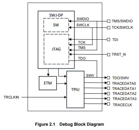
- Refer to the Debug Block Diagram (Figure 2.1) to better understand the interface.
- Ensure proper power supply and connections.
FAQs (Frequently Asked Questions)
- What are the properties of each bit in a register?
The properties are expressed as R (Read only), W (Write only), or R/W (Read and write). - How should be reserved bits of a register be handled?
Reserved bits must not be rewritten, and the read value should not be used. - How do we interpret numeric formats in the manual?
Hexadecimal numbers are prefixed with 0x, decimal numbers can have a suffix of 0d, and binary numbers can be prefixed with 0b.
Preface
Related Document
| Document name |
| Input/Output Ports |
| Product Information |
| Flash Memory |
| Clock Control and Operation Mode |
Conventions
- Numeric formats follow the rules as shown below:
- Hexadecimal: 0xABC
- Decimal: 123 or 0d123
Only when it needs to be explicitly shown that they are decimal numbers. - Binary: 0b111
It is possible to omit the “0b” when the number of bits can be distinctly understood from a sentence.
- “_N” is added to the end of signal names to indicate low active signals.
- It is called “assert” that a signal moves to its active level, and “deassert” to its inactive level.
- When two or more signal names are referred to, they are described as [m:n].
Example: S[3:0] shows four signal names S3, S2, S1 and S0 together. - The characters surrounded by [ ] define the register.
Example: [ABCD] - “N” substitutes the suffix number of two or more same kind of registers, fields, and bit names.
Example: [XYZ1], [XYZ2], [XYZ3] → [XYZn] - “x” substitutes the suffix number or character of units and channels in the register list.
- In the case of the unit, “x” means A, B, and C, …
Example: [ADACR0], [ADBCR0], [ADCCR0] → [ADxCR0] - In the case of the channel, “x” means 0, 1, and 2, …
Example: [T32A0RUNA], [T32A1RUNA], [T32A2RUNA] → [T32AxRUNA] - The bit range of a register is written as [m: n].
Example: Bit[3: 0] expresses the range of bit 3 to 0. - The configuration value of a register is expressed by either the hexadecimal number or the binary number.
Example: [ABCD]<EFG> = 0x01 (hexadecimal), [XYZn]<VW> = 1 (binary) - Word and byte represent the following bit length.
- Byte: 8 bits
- Half word: 16 bits
- Word: 32 bits
- Double word: 64 bits
- Properties of each bit in a register are expressed as follows:
- R: Read only
- W: Write only
- R/W: Read and write are possible.
- Unless otherwise specified, register access supports only word access.
- The register defined as “Reserved” must not be rewritten. Moreover, do not use the read value.
- The value read from the bit having a default value of “-” is unknown.
- When a register containing both of writable bits and read-only bits is written, read-only bits should be written with their default value, In the cases that default is “-“, follow the definition of each register.
- Reserved bits of the write-only register should be written with their default value. In the cases that the default is “-“, follow the definition of each register.
- Do not use read-modified-write processing to the register of a definition which is different by writing and read out.
Terms and Abbreviations
Some of abbreviations used in this document are as follows:
- SWJ-DP Serial Wire JTAG Debug Port
- ETM Embedded Trace MacrocellTM
- TPIU Trace Port Interface Unit
- JTAG Joint Test Action Group
- SW Serial Wire
- SWV Serial Wire Viewer
Outlines
The Serial Wire JTAG Debug Port (SWJ-DP) unit for interfacing with the debugging tools and the Embedded Trace Macrocell (ETM) unit for instruction trace output are built-in. Trace data is output to the dedicated pins(TRACEDATA[3:0], SWV) for the debugging via the on-chip Trace Port Interface Unit (TPIU).
| Function classification | Function | Operation |
| SWJ-DP | JTAG | It is possible to connect the JTAG support debugging tools. |
| SW | It is possible to connect the Serial Wire debugging tools. | |
| ETM | Trace | It is possible to connect the ETM Trace support debugging tools. |
For details about SWJ-DP, ETM and TPIU, refer to”Arm ® Cortex-M3 ® Processor Technical Reference Manual”/”Arm Cortex-M4 Processor Technical Reference Manual”.
Configuration
Figure 2.1 shows the block diagram of the debug interface.
| No. | Symbol | Signal name | I/O | Related reference manual |
| 1 | TRCLKIN | Trace Function Clock | Input | Clock Control and Operation Mode |
| 2 | TMS | JTAG Test Mode Selection | Input | Input/Output Ports, Product Information |
| 3 | SWDIO | Serial Wire Data Input/Output | Input/Output | Input/Output Ports, Product Information |
| 4 | TCK | JTAG Serial Clock input | Input | Input/Output Ports, Product Information |
| 5 | SWCLK | Serial Wire Clock | Input | Input/Output Ports, Product Information |
| 6 | TDO | JTAG Test Data Output | Output | Input/Output Ports, Product Information |
| 7 | SWV | Serial Wire Viewer Output | Output | Input/Output Ports, Product Information |
| 8 | TDI | JTAG Test Data Input | Input | Input/Output Ports, Product Information |
| 9 | TRST_N | JTAG Test RESET_N | Input | Input/Output Ports, Product Information |
| 10 | TRACEDATA0 | Trace Data 0 | Output | Input/Output Ports, Product Information |
| 11 | TRACEDATA1 | Trace Data 1 | Output | Input/Output Ports, Product Information |
| 12 | TRACEDATA2 | Trace Data 2 | Output | Input/Output Ports, Product Information |
| 13 | TRACEDATA3 | Trace Data 3 | Output | Input/Output Ports, Product Information |
| 14 | TRACECLK | Trace Clock | Output | Input/Output Ports, Product Information |
- SWJ-DP
- SWJ-DP supports the Serial Wire Debug Port (SWCLK, SWDIO), the JTAG Debug Port (TDI, TDO, TMS, TCK, TRST_N), and trace output from Serial Wire Viewer(SWV).
- When you use the SWV, please set an applicable clock enable bit to 1 (clock supply) in the Clock supply and stop register ([CGSPCLKEN]<TRCKEN>). For details, see the “Clock Control and Operation Mode” and “Input/Output Ports” of the reference manual.
- The JTAG Debug Port or TRST_N pin does not exist depending on the product. For details, see the “Product Information” of the reference manual.
- ETM
- ETM supports data signals to four pins(TRACEDATA) and one clock signal pin (TRACECLK).
- When you use the ETM, please set an applicable clock enable bit to 1 (clock supply) in the Clock supply and stop register ([CGSPCLKEN]<TRCKEN>). For details, see the “Clock Control and Operation Mode” and “Input/Output Ports” of the reference manual.
- ETM is not supported depending on the product. For details, see the “Product Information” of the reference manual.
Function and Operation
Clock Supply
When you use the Trace or SWV, please set an applicable clock enable bit to 1 (clock supply) in the ADC Trace Clock supply stop register ([CGSPCLKEN]<TRCKEN>). For details, see the “Clock Control and Operation Mode” of the reference manual.
Connection with Debug Tool
- Concerning a connection with debug tools, refer to manufactures’ recommendations. Debug interface pins contain a pull-up resistor and a pull-down resistor. When debug interface pins are connected with external pull-up or pulldown, please pay attention to input level.
- When the security function is enabled, the CPU cannot connect to the debug tool.
Peripheral Functions in Halt Mode
- The hold mode means that the state where the CPU is stopped (break) on the debugging tool
- When the CPU enters in the halt mode, the watchdog timer (WDT) automatically stops. Other peripheral functions continue to operate.
Usage Example
- The debug interface pins can also be used as general-purpose ports.
- After releasing reset, the particular pins of the debug interface pins are initialized as the debug interface pins. The other debug interface pins should be changed to the debug interface pins if needed.
Debug interface Debug interface pins JTAG TRST_N TDI TDO TCK TMS TRACEDATA [3:0] TRACECLK SW – – SWV SWCLK SWDIO Debug pins status after releasing reset
Valid
Valid
Valid
Valid
Valid
Invalid
Invalid
JTAG (With TRST_N)
✔ ✔ ✔ ✔ ✔ N/A N/A JTAG (Without TRST_N)
N/A
✔
✔
✔
✔
N/A
N/A
JTAG+TRACE ✔ ✔ ✔ ✔ ✔ ✔ ✔ SW N/A N/A N/A ✔ ✔ N/A N/A SW+TRACE N/A N/A N/A ✔ ✔ ✔ ✔ SW+SWV N/A N/A ✔ ✔ ✔ N/A N/A Debug function disable N/A N/A N/A N/A N/A N/A N/A
Precaution
Important Points of Using Debug Interface Pins Used as General-purpose Ports
- After releasing reset, if the debug interface pins are used as the general I/O ports by the user program, the debug tool cannot be connected.
- If the debug interface pins are used to other function, please pay attention of the settings.
- If the debug tool cannot be connected, it can recover debug connection to erase the flash memory using single BOOT mode from external. For details, please refer reference manual of “Flash Memory”.
Revision History
| Revision | Date | Description |
| 1.0 | 2017-09-04 | First release |
|
1.1 |
2018-06-19 |
– Contents
Modified Table of Contents to Contents -1 Outline Modified ARM to Arm. -2. Configuration Reference “reference manual” is added to SWJ-DP Reference “reference manual” is added to SWJ-ETM |
|
1.2 |
2018-10-22 |
– Conventions
Modified explanation of trademark – 4. Usage Example Added example for SW+TRACE in Table4.1 – Replaced RESTRICTIONS ON PRODUCT USE |
|
1.3 |
2019-07-26 |
– Figure 2.1 revised
– 2 Added clock setting for using SWV function. – 3.1 Added clock setting for using SWV function. modified from “ETM” to “Trace”. – 3.3 Added description of Hold mode. |
| 1.4 | 2024-10-31 | – Appearance updated |
RESTRICTIONS ON PRODUCT USE
Toshiba Corporation and its subsidiaries and affiliates are collectively referred to as “TOSHIBA”.
Hardware, software and systems described in this document are collectively referred to as “Products”.
- TOSHIBA reserves the right to make changes to the information in this document and related Products without notice.
- This document and any information herein may not be reproduced without prior written permission from TOSHIBA. Even with TOSHIBA’s written permission, reproduction is permissible only if reproduction is without alteration/omission.
- Though TOSHIBA works continually to improve the Product’s quality and reliability, the Product can malfunction or fail. Customers are responsible for complying with safety standards and for providing adequate designs and safeguards for their hardware, software, and systems which minimize risk and avoid situations in which a malfunction or failure of a Product could cause loss of human life, bodily injury or damage to property, including data loss or corruption. Before customers use the Product, create designs including the Product, or incorporate the Product into their own applications, customers must also refer to and comply with (a) the latest versions of all relevant TOSHIBA information, including without limitation, this document, the specifications, the data sheets and application notes for Product and the precautions and conditions outlined in the “TOSHIBA Semiconductor Reliability Handbook” and (b) the instructions for the application with which the Product will be used with or for. Customers are solely responsible for all aspects of their product design or applications, including but not limited to (a) determining the appropriateness of the use of this Product in such design or applications; (b) evaluating and determining the applicability of any information contained in this document, or in charts, diagrams, programs, algorithms, sample application circuits, or any other referenced documents; and (c) validating all operating parameters for such designs and applications. TOSHIBA ASSUMES NO LIABILITY FOR CUSTOMERS’ PRODUCT DESIGN OR APPLICATIONS.
- PRODUCT IS NEITHER INTENDED NOR WARRANTED FOR USE IN EQUIPMENT OR SYSTEMS THAT REQUIRE EXTRAORDINARILY HIGH LEVELS OF QUALITY AND/OR RELIABILITY, AND/OR A MALFUNCTION OR FAILURE OF WHICH MAY CAUSE LOSS OF HUMAN LIFE, BODILY INJURY, SERIOUS PROPERTY DAMAGE, AND/OR SERIOUS PUBLIC IMPACT (“UNINTENDED USE”). Except for specific applications as expressly stated in this document, Unintended Use includes, without limitation, equipment used in nuclear facilities, equipment used in the aerospace industry, medical equipment, equipment used for automobiles, trains, ships, and other transportation, traffic signaling equipment, equipment used to control combustions or explosions, safety devices, elevators and escalators, devices related to electric power, and equipment used in finance-related fields. IF YOU USE THE PRODUCT FOR UNINTENDED USE, TOSHIBA ASSUMES NO LIABILITY FOR THE PRODUCT. For details, please contact your TOSHIBA sales representative.
- Do not disassemble, analyze, reverse-engineer, alter, modify, translate or copy Product, whether in whole or in part.
- Product shall not be used for or incorporated into any products or systems whose manufacture, use, or sale is prohibited under any applicable laws or regulations.
- The information contained herein is presented only as guidance for Product use. No responsibility is assumed by TOSHIBA for any infringement of patents or any other intellectual property rights of third parties that may result from the use of the Product. No license to any intellectual property right is granted by this document, whether express or implied, by estoppel or otherwise.
- ABSENT A WRITTEN SIGNED AGREEMENT, EXCEPT AS PROVIDED IN THE RELEVANT TERMS AND CONDITIONS OF SALE FOR THE PRODUCT, AND TO THE MAXIMUM EXTENT ALLOWABLE BY LAW, TOSHIBA (1) ASSUMES NO LIABILITY WHATSOEVER, INCLUDING WITHOUT LIMITATION, INDIRECT, CONSEQUENTIAL, SPECIAL, OR INCIDENTAL DAMAGES OR LOSS, INCLUDING WITHOUT LIMITATION, LOSS OF PROFITS, LOSS OF OPPORTUNITIES, BUSINESS INTERRUPTION AND LOSS OF DATA, AND (2) DISCLAIMS ANY AND ALL EXPRESS OR IMPLIED WARRANTIES AND CONDITIONS RELATED TO SALE, USE OF PRODUCT, OR INFORMATION, INCLUDING WARRANTIES OR CONDITIONS OF MERCHANTABILITY, FITNESS FOR A PARTICULAR PURPOSE, ACCURACY OF INFORMATION, OR NONINFRINGEMENT.
- Do not use or otherwise make available Product or related software or technology for any military purposes, including without limitation, for the design, development, use, stockpiling or manufacturing of nuclear, chemical, or biological weapons or missile technology products (mass destruction weapons). Product and related software and technology may be controlled under the applicable export laws and regulations including, without limitation, the Japanese Foreign Exchange and Foreign Trade Law and the U.S. Export Administration Regulations. Export and re-export of Product or related software or technology are strictly prohibited except in compliance with all applicable export laws and regulations.
- Please contact your TOSHIBA sales representative for details as to environmental matters such as the RoHS compatibility of Product. Please use the Product in compliance with all applicable laws and regulations that regulate the inclusion or use of controlled substances, including without limitation, the EU RoHS Directive. TOSHIBA ASSUMES NO LIABILITY FOR DAMAGES OR LOSSES OCCURRING AS A RESULT OF NONCOMPLIANCE WITH APPLICABLE LAWS AND REGULATIONS.
Toshiba Electronics Devices & Storage Corporation: https://toshiba.semicon-storage.com/
Documents / Resources
 |
TOSHIBA DEBUG-A 32 Bit RISC Microcontroller [pdf] Instructions DEBUG-A 32 Bit RISC Microcontroller, DEBUG-A, 32 Bit RISC Microcontroller, RISC Microcontroller, Microcontroller |


