Suzhou Pairlink Network Technology Buffalo-DS531 Bluetooth 5.1 BLE Module

Electrical Specifications
Absolute Ratings
|
Parameter |
Specification |
Unit |
|
| Min. | Max. | ||
| Power Supply(V) | -0.3V | +3.6V | Burn the module permanently
if it exceeds +3.6V |
| Storage temperature(℃) | -40 | +125 | |
| Working temperature(℃) | -40 | +85 | |
| ESD HBM | -4KV | +4KV | Human Body Model |
| ESD CDM | -500V | +500V | Charged-Device Model |
Recommended Operating Conditions
|
Parameter |
Specification |
Note |
|||
| Min. | Typical | Max. | |||
| Power Supply(V) | 1.8 | 3.3 | 3.6 | ||
| Communication level(V) | 3.3 | Can’t communicate with 5V TTL
level directly |
|||
| Working temperature(℃) | -40 | 20 | +85 | Industry Standard | |
| TX Current
(mA) |
3.5 | TX Power=+2.5dBm | |||
| Consume | RX Current
(mA) |
2.2 | 1Mbps | ||
| Sleep Current
(uA) |
2 | Software off period | |||
| TX Power(dBm) | -19.5 | +2.5 | |||
| Receive Sensitivity(dBm) | -94 | 1Mbps | |||
Physical Parameters
| Parameter | Performance | Note | |
|
Distance |
Buffalo-DS531-B |
30m |
Data Transfer (BLE) Environment: Sunny and open Airspeed: 1Mbps
Buffalo-DS531-B with PCB antenna |
| Crystal | 32MHz | Industry Standard | |
| Protocol | Bluetooth 5.1 | Supported data rates: 1 Mbps | |
| Package | Patch | Refer to section 4.3 | |
| IC | DA14531-00000FX2 | Package:FCGQFN24 | |
| Core | ARM Cortex-M0 | ||
| OTP | 32KB | One-Time-Programmable | |
| RAM | 48KB | ||
| ROM | 144KB | ||
| EEPROM | Buffalo-DS531-B:2Kbit | Type:P24C02A | |
| Dimensions(mm) | 16.3*12.0*2.4 | L*W*H | |
| Antenna Type | Buffalo-DS531-B | On-board PCB antenna | |
| Antenna Gain | +0dbi | On-board PCB antenna | |
Peripheral Interface
- 2 x UARTs (one with flow control)
- 1 x SPI interface with master configurable
- 1 x I2Cs interface
- 12 x GPIOs
- 4 x 10-bit ADC input
- 8 x PWMs interface
- 2 x general-purpose timer
Hardware Design and PCB layout
Pin assignment and Pin description: Buffalo DS 531 B Pin definition can refer to Figure 1
Table 1: Module Pin Description
| Pin Number | Pin Name | I/O | RESET STATE | Alternate Function Description | |
| 8 | VBAT | P | Power Supply | ||
| 1,15,16 | GND | P | Connect to Ground | ||
| P0_0 | DIO | I-PD | GPIO:P0_0 | ||
| 6
Reset |
DI | I-PD | Reset signal (active high). | ||
| P0_6 | DIO | ||||
| 2 | ADC2 | AI | I-PD | ||
| P0_2 | DIO | ||||
| 3 SWCLK | DIO | I-PD | |||
| ADC1 | AI | ||||
INPUT/OUTPUT with selectable pulls up/down resistor. General purpose I/O port bit or alternate function nodes. Contain state retention mechanism during power down.
Reference Design
The latest schematic and design examples, bill of material, and layout file are available from the original developer Contact us for details.

Circuit Description
- VBAT supply voltage value is 1.80V 3.60V.
- PIN10 (P0_9 / UART_RX), and PIN11(P0.8 / UART_TX) are configured as the module’s UART interface by default.
- PIN 6 ( 0 /RESET) multiple xing module RESET, the software can be configured as RESET function, int ernal pull down by default. If need to configure the RESET function must consult the Pair link for recommendations.
- The Buffalo DS531 B is TTL level, and the UART port can communicate directly with the 3.3V MCU.
- Support GPIO super multiplexing function, WAKE_ UP / UART / SPI / IIC / PWM /, and other functions can be arbitrarily configured on GPIO.
- Reserve P1 burning interface if the PCB board has enough space.
- The application diagram is shown below.

Appearance and Dimensions
Figure 2 shows the size of the module. The components and prominent structure are not allowed put in this size range(16.3mm*12.0mm*2.4mm). The following land pattern size is recommended for user board design. However, the user can modify it according PC B soldering conditions. Sufficient examination is necessary if using the modified land pattern.
Module Layout Guideline
The layout on the user PCB should be designed according to the following guideline. When the module is placed on the PCB, it must be ensured that the RF antenna area (2 times the width of the module) is hollow or suspended, and there must be no traces, vias, or copper.
Welding Declaration
The Buffalo-DS531-B module only supports one reflow soldering. Our company is not responsible for the module failure caused by multiple reflow soldering.
Figure 4:Reflow Soldering Temperature
Figure 5 Reflow Soldering Curve

Federal Communications Commission (FCC) Interference Statement
This equipment has been tested and found to comply with the limits for a Class B digital device, pursuant to Part15 of the FCC Rules. These limits are designed to provide reasonable protection against harmful interference in a residential installation. This equipment generates, uses, and can radiate radio frequency energy and, if not installed and used in accordance with the instructions, may cause harmful interference to radio communications. However, there is no guarantee that interference will not occur in a particular installation. If this equipment does cause harmful interference to radio or television reception, which can be determined by turning the equipment off and on, the user is encouraged to try to correct the interference by one of the following measures:
- Reorient or relocate the receiving
- Increase the separation between the equipment and
- Connect the equipment into an outlet on a circuit different from that to which the receiver is
- Consult the dealer or an experienced radio/TV technician for an experienced radio/TV technician for help.
This device complies with Part 15 of the FCC Rules. Operation is subject to the following two conditions:
- This device may not cause harmful interference, and
- this device must accept any interference received, including interference that may cause undesired operation.
FCC Caution: Any changes or modifications not expressly approved by the party responsible for compliance could void the user’s authority to operate this equipment.
The module is limited to OEM installation only This product is mounted inside of the end product only by professional installers OEM. They use this module with changing the power and control signal setting by software of end product within the scope of this application. End-user cannot change this setting. The OEM integrator has to be aware no to provide information to the end-user regarding how to install or remove this RF module in the user manual of the end product with integrates this module. The end-user manual shall include all required regulatory information/warning as shown in this manual. That separate approval is required for all other operating configurations, including portable configurations with respect to Part 2.1093 and different antenna configurations.
RF exposure warning
This equipment complies with FCC radiation exposure limits set forth for an uncontrolled environment. This product may not be collocated or operated in conjunction with any other antenna or transmitter This equipment must be installed and operated in accordance with provided instructions and the antenna(s) used for this transmitter must be installed to provide a separation distance of at least 20 cm from all persons and must not be collocated or oper ating in conjunction with any other antenna or transmitter.
Industry Canada
(IC) CAN ICES 3 (B)/NMB 3(B)
This device complies with Industry Canada’s license-exempt RSS. Operation is subject to the following two conditions:
- This device may not cause harmful interference, and this device must accept any interference received, including interference that may cause undesired operation.
IMPORTANT NOTE
Radiation Exposure Statement:
This equipment complies with IC radiation exposure limits set forth for an uncontrolled environment. This equipment should be installed and operated with a minimum distance of 20cm between the radiator and your body.
OEM Integration Instructions
This device is intended only for OEM integrators under the fol lowing conditions The module can be used to install in another host, and the transmitter module may not be co-located with any other transmitter or antenna. The module shall be only used with the integral antenna(s) that has been originally tested and certified with this module. As long as 3 conditions above are transmitter tests will not be required. However, the OEM integrator is still responsible for testing their end-product for any additional compliance requirement with this module installed (for example, digital device emission, PC peripheral requirements, etc.)
IMPORTANT NOTE
In the event that these conditions cannot be met (for example certain laptop configuration or c o location with another transmitter), then the FCC authorization for this module in combination with the host equipment is no longer considered valid and the FCC ID of the module cannot be used on the final product. In this circumstance, the OEM integrator will be responsible for re-evaluating. The end product (including the transmitter) and obtaining a separate FCC authorization. The final end product must be labeled in a visible area with the following:
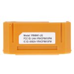
Contains Transmitter Module FCC ID: 2AQV6BDS531
Antenna Specification
|
Antenna Type |
Manufacturer |
Frequency Range
(MHz) |
Maximum Peak
Antenna Gain(dBi) |
| PCB Antenna | N/A | 2402 – 2480 | -0.41dBi |
IMPORTANT NOTE
This Wireless Module IC: 24210 BDS531 ) has been approved by Industry Canada to operate with the antenna types listed below with the maximum permissible gain indicated. Antenna types not included in this list, having a gain greater than the maximum gain indicated for that type, are strictly prohibited for use with this device. The Host Marketing Name (HMN) must be displayed (according to e-labeling requirements) or indicated at any location on the exterior of the host product or product packaging or product literature, which shall be available with the host product or online. The host product shall be properly labeled to identify the modules within the host product. The Innovation,
Science, and Economic Development
Canada certification label of a module shall be clearly visible at all times when installed in the host product; otherwise, the host product must be labeled to display the Innovation, Science, and Economic Development Canada certification number for the module, preceded by the word “Contains” or similar wording expressing the same meaning, as follows:
Contains IC: 2421 0 BDS531
Antenna Specification
|
Antenna Type |
Manufacturer |
Frequency Range
(MHz) |
Maximum Peak
Antenna Gain(dBi) |
| PCB Antenna | N/A | 2402 – 2480 | -0.41dBi |
Documents / Resources
 |
Suzhou Pairlink Network Technology Buffalo-DS531 Bluetooth 5.1 BLE Module [pdf] User Guide BDS531, 2AQV6BDS531, Buffalo-DS531 Bluetooth 5.1 BLE Module, Buffalo-DS531, Bluetooth 5.1 BLE Module |
 |
Suzhou Pairlink Network Technology Buffalo-DS531 Bluetooth 5.1 BLE Module [pdf] User Guide BDS531, 2AQV6BDS531, Buffalo-DS531 Bluetooth 5.1 BLE Module, Buffalo-DS531, Bluetooth 5.1 BLE Module |