Rockchip CM3568 Boardcon Embedded Design User Manual

Introduction
About this Manual
This manual is intended to provide the user with an overview of the board and benefits, complete features specifications, and set up procedures. It contains important safety information as well.
Feedback and Update to this Manual
To help our customers make the most of our products, we are continually making additional and updated resources available on the Boardcon website (www.boardcon.com , www.armdesigner.com).
These include manuals, application notes, programming examples, and updated software and hardware. Check in periodically to see what’s new!
When we are prioritizing work on these updated resources, feedback from customers is the number one influence, If you have questions, comments, or concerns about your product or project, please no hesitate to contact us at support@armdesigner.com.
Limited Warranty
Boardcon warrants this product to be free of defects in material and workmanship for a period of one year from date of buy. During this warranty period Boardcon will repair or replace the defective unit in accordance with the following process:
A copy of the original invoice must be included when returning the defective unit to Boardcon. This limited warranty does not cover damages resulting from lighting or other power surges, misuse, abuse, abnormal conditions of operation, or attempts to alter or modify the function of the product.
This warranty is limited to the repair or replacement of the defective unit. In no event shall Boardcon be liable or responsible for any loss or damages, including but not limited to any lost profits, incidental or consequential damages, loss of business, or anticipatory profits arising from the use or inability to use this product.
Repairs make after the expiration of the warranty period are subject to a repair charge and the cost of return shipping. Please contact Boardcon to arrange for any repair service and to obtain repair charge information.
CM3568 Introduction
Summary
The CM3568 system-on-module is equipped with Rockchip’s RK3568 with quad-core Cortex-A55 CPU, Mali-G52 GPU, and 1 TOPs NPU.
It is designed specifically for the AI devices such as industrial controller, IoT devices, intelligent interactive devices, personal computers and robots. The high performance and low power solution can help customers to introduce new technologies more quickly and enhance the overall solution efficiency.

Features
- Microprocessor
- Quad-core Cortex-A55 up to 1.8GHz
- 32KB I-cache and 32KB D-cache for each core, 512KB L3 cache
- 1 TOPS Neural Process Unit
- Mali-G52 up to 0.8GHz
- Memory Organization
- LPDDR4 or LPDDR4X RAM up to 8GB
- EMMC up to 128GB
- Boot ROM
- Supports system code download through USB OTG or SD
- Trust Execution Environment system
- Supports secure OTP and multiple cipher engine
- Video Decoder/Encoder
- Supports video decoding up to 4K@60fps
- Supports H.264 encode
- H.264 HP encoding up to 1080p@100fps
- Picture size up t0 8192×8192
- Display Subsystem
- Video Output
Supports HDMI 2.0 transmitter with HDCP 1.4/2.2, up to 4K@60fps
Supports 8/4 lanes MIPI DSI up to 2560×1440@60Hz Or LVDS interface up to 1920×1080@60Hz
Supports ePD1.3 interface up to 2560×1600@60fps
Supports BT-656 8bit output
Supports BT-1120 16bit output
Support 24bits RGB TTL output
Support three display with different source - Image Input
Supports MIPI CSI 4lanes interface Or 2ch MIPI CSI 2lanes interfaces
- Video Output
- I2S/PCM/ AC97
- Three I2S/PCM interfaces
- Support Mic array Up to 8ch PDM/TDM interface
- One SPDIF output
- USB and PCIE
- Three 2.0 USB interfaces
- One USB 2.0 OTG+SATA or 3.0 USB hosts
- One USB 3.0 host or SATA interface.
- One 1lane PCIE or SATAI interface.
- Ethernet
- One GMAC/EMAC and QSGMII
- Support 10/100/1000Mbit/s data transfer rates
- Support MII/RGMII PHY interface
- I2C
- Up to Five I2C
- Support standard mode and fast mode(up to 400kbit/s)
- SDIO
- Support SDIO 3.0 protocol
- SPI
- Up to four SPI controllers,
- Full-duplex synchronous serial interface
- UART
- Support up to 9 UARTs
- UART2 with 2 wires for debug tools
- Embedded two 64byte FIFO
- Support auto flow control mode for UART1-5
- SATA
- Three SATA host controller
- Support SATA 1.5Gb/s, 3.0Gb/s and SATA 6.0Gb/s
- ADC
- Up to Three ADC channels
- 10-bit resolution
- Voltage input range between 0V to 1.8V
- Support up to 1MS/s sampling rate
- PWM
- 14 on-chip PWMs with interrupt-based operation
- Support 32bit time/counter facility
- IR option on PWM3/7/11/15
- Analog Audio
- 1.3W@8 ohm Speaker output
- Headphone stereo output
- Stereo MIC input
- Power unit
- PMU with audio codec on board
- 5V and 3.3V input or Single 3.3V input
- 1.8V max 500mA output
- Very low RTC consume current, less 5uA at 3V button Cell
CM3568 Block Diagram
RK3568 Block Diagram

Development board (EM3568) Block Diagram

CM3568 specifications
| Feature | Specifications |
| CPU | Quad-core Cortex-A55 |
| DDR | 2GB (up to 8GB) |
| eMMC FLASH | 8GB (up to 128GB) |
| Power | DC 3.3V or DC 5V&3.3V |
| LVDS/MIPI DSI | 1-CH LVDS or MIPI, 2-CH MIPI DSI |
| I2S | 3-CH |
| MIPI CSI | 1-CH 4-Lane or 2-CH 2-Lane CSI |
| SATA | 3-CH |
| HDMI out | 1-CH |
| CAN | 2-CH |
| USB | 3-CH (USB HOST2.0), 1-CH(OTG 2.0) and 1-CH(USB 3.0) |
| Ethernet | 2-ch GMAC: GMDI, GMII and QSGMIIIf GMII is not needed, it can be set to SDIO, UART and PCM for WIFI/BT module. |
| SDMMC | 2-CH |
| SPDIF TX | 1-CH |
| I2C | 5-CH |
| SPI | 4-CH |
| UART | 8-CH, 1-CH(DEBUG) |
| PWM | 14-CH |
| ADC IN | 3-CH |
| Board Dimension | 60 x 45mm |
CM3568 PCB Dimension

CM3568 Pin Definition
| Pin | Signal | Description or functions | GPIO serial | IO Voltage |
| 1 | HDMI_TX0N_PORT | 0.5V | ||
| 2 | HDMI_TX0P_PORT | 0.5V | ||
| 3 | HDMI_TX1N_PORT | 0.5V | ||
| 4 | HDMI_TX1P_PORT | 0.5V | ||
| 5 | HDMI_TX2N_PORT | 0.5V | ||
| 6 | HDMI_TX2P_PORT | 0.5V | ||
| 7 | HDMI_TX_HPDIN | HDMI hot plug detect signal | 3.3V | |
| 8 | PCIE20_REFCLKP | PCIE2 reference clock output | 0.5V | |
| 9 | PCIE20_REFCLKN | PCIE2 reference clock output | 0.5V | |
| 10 | PCIE20_RXP | PCIE2/SATA/QSGMII RXP | 0.5V | |
| 11 | PCIE20_RXN | PCIE2/SATA/QSGMII RXN | 0.5V | |
| 12 | PCIE20_TXP | PCIE2/SATA/QSGMII TXP | 0.5V | |
| 13 | PCIE20_TXN | PCIE2/SATA/QSGMII TXN | 0.5V | |
| 14 | USB3_HOST1_SSTXN | USB3/SATA/QSGMII TXN | 0.5V | |
| 15 | USB3_HOST1_SSTXP | USB3/SATA/QSGMII TXP | 0.5V | |
| 16 | USB3_HOST1_SSRXN | USB3/SATA/QSGMII RXN | 0.5V | |
| 17 | USB3_HOST1_SSRXP | USB3/SATA/QSGMII RXP | 0.5V | |
| 18 | USB3_OTG0_SSTXN | USB3 OTG or SATA TXN | 0.5V | |
| 19 | USB3_OTG0_SSTXP | USB3 OTG or SATA TXP | 0.5V | |
| 20 | USB3_OTG0_SSRXN | USB3 OTG or SATA RXN | 0.5V | |
| 21 | USB3_OTG0_SSRXP | USB3 OTG or SATA RXP | 0.5V | |
| 22 | GND | Ground | 0V | |
| 23 | USB3_HOST1_DM | USB3 Host1 DM | 0.5V | |
| 24 | USB3_HOST1_DP | USB3 Host1 DP | 0.5V | |
| 25 | USB3_OTG0_DP | USB3 OTG0 DP | 0.5V | |
| 26 | USB3_OTG0_DM | USB3 OTG0 DM | 0.5V | |
| 27 | UART1_RTSn_M0/GMAC0_TXEN | GMAC0_TXEN /UART1_RTSor SPI1_CLK_M0 | GPIO2_B5_u | 1.8V |
| 28 | UART1_TX_M0/GMAC0_TXD1 | GMAC0_TXD1 orUART1_TXD | GPIO2_B4_u | 1.8V |
| 29 | UART1_RX_M0/GMAC0_TXD0 | GMAC0_TXD0 orUART1_RXD | GPIO2_B3_u | 1.8V |
| 30 | BT_REG_ON_H_GPIO2_B7/GMAC0_RXD1 | GMAC0_RXD1/I2S2_SCK_RX_M0 or SPI1_MOSI_M0 | GPIO2_B7_d | 1.8V |
| 31 | UART1_CTSn_M0/GM AC0_RXD0 | GMAC0_RXD0/UART1_CTS or SPI1_MISO_M0 | GPIO2_B6_u | 1.8V |
| 32 | SDMMC1_D1/GMAC0_RXD3 | GMAC0_RXD3/SDMMC1_D1 or UART6_TX_M0 | GPIO2_A4_u | 1.8V |
| 33 | SDMMC1_D0/GMAC0_RXD2 | GMAC0_RXD2/SDMMC1_D0 or UART6_RX_M0 | GPIO2_A3_u | 1.8V |
| 34 | SDMMC1_CLK/GMAC0_TXCLK | GMAC0_TXCLK/SDMMC1_CLK or UART9_TX_M0 | GPIO2_B0_d | 1.8V |
| 35 | SDMMC1_CMD/GMAC0_TXD3 | GMAC0_TXD3/SDMMC1_CMD or UART9_RX_M0 | GPIO2_A7_u | 1.8V |
| 36 | SDMMC1_D3/GMAC0_TXD2 | GMAC0_TXD2/SDMMC1_D3or UART7_TX_M0 | GPIO2_A6_u | 1.8V |
| 37 | SDMMC1_D2/GMAC0_RXCLK | GMAC0_RXCLK/SDMMC1_D2 or UART7_RX_M0 | GPIO2_A5_u | 1.8V |
| 38 | GND | Ground | 0V | |
| 39 | SOC_PCM_CLK/GMAC0_MCLKINOUT | GMAC0_MCLK/I2S2_SCKTx/UART7CTS/SPI2_MISO_M0 | GPIO2_C2_d | 1.8V |
| 40 | SOC_PCM_SYNC/GMAC0_MDC | GMAC0_MDC/I2S2_LRCKTx/UART7RTS/SPI2_MOSI_M0 | GPIO2_C3_d | 1.8V |
| 41 | SOC_PCM_OUT/GMAC0_MDIO | GMAC0_MDIO/I2S2_SDO/UART9CTS/SPI2_CS0_M0 | GPIO2_C4_d | 1.8V |
| 42 | BT_WAKE_HOST_H/GMAC0_RXDV_CRS | GMAC0_RXDV/I2S2_LRCKRx/UART6CTS/SPI1CS0_M0 | GPIO2_C0_d | 1.8V |
| 43 | HOST_WAKE_BT_H_GPIO2_C1 | I2S2_MCLK/UART7_RTS/SPI2_CLK_M0 | GPIO2_C1_d | 1.8V |
| 44 | EDP_TX_D3N | 0.5V | ||
| 45 | EDP_TX_D3P | 0.5V | ||
| 46 | EDP_TX_D2N | 0.5V | ||
| 47 | EDP_TX_D2P | 0.5V | ||
| 48 | EDP_TX_D1N | 0.5V | ||
| 49 | EDP_TX_D1P | 0.5V | ||
| 50 | EDP_TX_D0N | 0.5V | ||
| 51 | EDP_TX_D0P | 0.5V | ||
| 52 | EDP_TX_AUXN | 0.5V | ||
| 53 | EDP_TX_AUXP | 0.5V | ||
| 54 | USB3_OTG0_VBUSDET | USB OTG VBUS detect input | 3.3V | |
| 55 | USB3_OTG0_ID | USB OTG ID input | 3.3V | |
| 56 | SDMMC0_CLK | UART5Tx_M0/CAN0_Rx_M1 | GPIO2_A2_d | 3.3V |
| 57 | SDMMC0_CMD | UART5Rx_M0/CAN0_Tx_M1 | GPIO2_A1_u | 3.3V |
| 58 | SDMMC0_D0 | UART6_Tx_M1/PWM8_M1 | GPIO1_D5_u | 3.3V |
| 59 | SDMMC0_D1 | UART6_Rx_M1/PWM9_M1 | GPIO1_D6_u | 3.3V |
| 60 | SDMMC0_D2 | UART5CTS_M0/JTAG_TCK | GPIO1_D7_u | 3.3V |
| 61 | SDMMC0_D3 | UART5RTS_M0/JTAG_TMS | GPIO2_A0_u | 3.3V |
| 62 | GND | Ground | 0V | |
| 63 | SARADC_VIN3 | 1.8V | ||
| 64 | SARADC_VIN2_HP_HOOK | 1.8V | ||
| 65 | SARADC_VIN0_KEY/RECOVERY | Program need short to GNDwhen power on.( Pull up 10K) | 1.8V | |
| 66 | GND | Ground | 0V | |
| 67 | GPIO2_C6 | UART8_Rx/SPI1_CS1_M0 | GPIO2_C6_d | 1.8V |
| 68 | WIFI_REG_ON_H_GPIO2_B1 | UART8_RTS_M0/CAN2_Rx_M1 | GPIO2_B1_d | 1.8V |
| 69 | WIFI_WAKE_HOST_H_GPIO2_B2 | UART8_CTS_M0/CAN2_Tx_M1/SD1_DET | GPIO2_B2_u | 1.8V |
| 70 | SOC_PCM_IN | UART8Tx_M0/I2S2_SDI_M0 | GPIO2_C5_d | 1.8V |
| 71 | UART0_TX/GPIO0_C1 | PWM2_M0/MCU_JTAG_TDI | GPIO0_C1_d | 3.3V |
| 72 | UART0_RX/PWM1_M0 | GPIO0_C0_d | 3.3V | |
| 73 | I2C1_SCL/CAN0_TX_M0 | PCIE30X1_ButtonRSTn/MCU_JTAG_TDO | GPIO0_B3_u (Pull up2.2K onboard) | 3.3V |
| 74 | I2C1_SDA/CAN0_RX_M0 | PCIE20_ButtonRSTn/MCU_JTAG_TCK | GPIO0_B4_u (Pull up2.2K onboard) | 3.3V |
| 75 | UART2TX_M0_DEBUG | Debug UART | GPIO0_D1_u | 3.3V |
| 76 | UART2RX_M0_DEBUG | Debug UART | GPIO0_D0_u | 3.3V |
| 77 | TP_INT_L_PWM1_M1 | SPI0_CLK _M0 | GPIO0_B5_u | 3.3V |
| 78 | LCD0_BL_PWM4 | PCIE30X1_PERSTn_M0 | GPIO0_C3_d | 3.3V |
| 79 | PCIE20_CLKREQn_M0/GPIO0_A5 | SDMMC0_PWREN/SATA_MP_SWITCH | GPIO0_A5_d | 3.3V |
| 80 | PWM3_IR | PCIE30X1_Wake/EDP_HPD | GPIO0_C2_d | 3.3V |
| 81 | LCD1_PWREN_H_GPIO0_C5 | PCIE30X2_WAKEn_M0/PWM6 /SPI0_MISO_M0 | GPIO0_C5_d | 3.3V |
| 82 | SDMMC0_DET_L | PCIE30X1_CLKREQn_M0 | GPIO0_A4_u | 3.3V |
| 83 | LCD1_BL_PWM5 | UART0_RTS/SPI0_CS1_M0 | GPIO0_C4_d | 3.3V |
| 84 | TP_RST_L_PWM2_M1 | SPI0_MOSI_M0 | GPIO0_B6_u | 3.3V |
| 85 | I2C4_SCL_M0 | SPI3CLK_M0/I2S2_SDO_M1(Pull up 2.2K onboard) | GPIO4_B3_d | 1.8V |
| 86 | I2C4_SDA_M0 | SPI3MOSI_M0 /I2S2SDI_M1(Pull up 2.2K onboard) | GPIO4_B2_d | 1.8V |
| 87 | I2C2_SCL_M1 | CAN2Tx_M0 /I2S1SDO3_M1(Pull up 2.2K onboard) | GPIO4_B5_d | 1.8V |
| 88 | I2C2_SDA_M1 | CAN2Rx_M0/ISP_Flash_Trig(Pull up 2.2K onboard) | GPIO4_B4_d | 1.8V |
| 89 | PDM_CLK1_M0_ADC | SPDIF_M0/UART4_Rx_M0 | GPIO1_A4_d | 3.3V |
| 90 | PDM_SDI1_M0_ADC | PCIE20_PERSTn_M2 | GPIO1_B2_d | 3.3V |
| 91 | PDM_SDI2_M0_ADC | PCIE20_WAKEn_M2 | GPIO1_B1_d | 3.3V |
| 92 | PDM_SDI3_M0_ADC | PCIE20_CLKREQn_M2 | GPIO1_B0_d | 3.3V |
| 93 | I2C3_SCL_M0 | (Pull up 2.2K onboard) | 3.3V | |
| 94 | I2C3_SDA_M0 | (Pull up 2.2K onboard) | 3.3V | |
| 95 | GND | Ground | 0V | |
| 96 | USB2_HOST2_DM | 1.8V | ||
| 97 | USB2_HOST2_DP | 1.8V | ||
| 98 | USB2_HOST3_DM | 1.8V | ||
| 99 | USB2_HOST3_DP | 1.8V | ||
| 100 | PHY1_LED2/CFG_LDO1 | Ethernet Speed LED(PU4.7K) | 3.3V | |
| 101 | PHY1_LED1/CFG_LDO0 | Ethernet Link LED(PD 4.7K) | 3.3V | |
| 102 | PHY1_MDI0+ | 0.5V | ||
| 103 | PHY1_MDI0- | 0.5V | ||
| 104 | PHY1_MDI1+ | 0.5V | ||
| 105 | PHY1_MDI1- | 0.5V | ||
| 106 | PHY1_MDI2+ | 0.5V | ||
| 107 | PHY1_MDI2- | 0.5V | ||
| 108 | PHY1_MDI3+ | 0.5V | ||
| 109 | PHY1_MDI3- | 0.5V | ||
| 110 | GND | Ground | 0V | |
| 111 | CIF_CLKOUT/PWM11_IR_M1/GPIO4_C0_d | GPIO4_C0_d | 1.8V | |
| 112 | UART7_TX_M1 | PDM_CLK1_M2/PWM14_M0 | GPIO3_C4_d | 3.3V |
| 113 | UART7_RX_M1 | SPDIFO_M1/PWM15_IR_M0 | GPIO3_C5_d | 3.3V |
| 114 | LCDC_VSYNC/UART5_TX_M1 | SPI1_MISO_M1/VOP_BT1120_D14 | GPIO3_C2_d | 3.3V |
| 115 | LCDC_HSYNC/PCIE20_PERSTn_M1 | SPI1_MOSI_M1/VOP_BT1120_D13 | GPIO3_C1_d | 3.3V |
| 116 | LCDC_DEN/UART5_RX_M1 | SPI1_CLK_M1/VOP_BT1120_D15 | GPIO3_C3_d | 3.3V |
| 117 | RTC32KOUT_WIFI | 32.768KHz output(PU 10K) | Open Drain | 3.3V |
| 118 | SPKP_OUT | 1.3W@8Ohm Speaker output | 1.8V | |
| 119 | SPKN_OUT | 1.3W@8Ohm Speaker output | 1.8V | |
| 120 | HPL_OUT | Headphone L-CH output | 1.8V | |
| 121 | HPR_OUT | Headphone R-CH output | 1.8V | |
| 122 | MIC1_INN | MIC1 P or MIC_L input | 1.8V | |
| 123 | MIC1_INP | MIC1 N or MIC_R input | 1.8V | |
| 124 | VRTC | RTC button Cell Power input | 3.0V | |
| 125 | LCDC_D23/UART3_RX_M1 | PDM_SDI3_M2 /PWM13_M0 | GPIO3_C0_d | 3.3V |
| 126 | LCDC_D22/UART3_TX_M1 | PDM_SDI2_M2 /PWM12_M0 | GPIO3_C0_d | 3.3V |
| 127 | LCDC_D21/PWM11_IR_M0 | VOP_BT1120_D12 | GPIO3_B6_d | 3.3V |
| 128 | LCDC_D20/GPIO3_B5 | VOP_BT1120_D11/PWM10_M0 | GPIO3_B5_d | 3.3V |
| 129 | LCDC_D19/I2C5_SDA_M0 | VOP_BT1120_D10/PDM_SDI1_M2 | GPIO3_B4_d | 3.3V |
| 130 | LCDC_D18/I2C5_SCL_M0 | VOP_BT1120_D9/PDM_SDI0_M2 | GPIO3_B3_d | 3.3V |
| 131 | LCDC_D17/UART4_TX_M1 | VOP_BT1120_D8/PWM9_M0 | GPIO3_B2_d | 3.3V |
| 132 | LCDC_D16/UART4_RX_M1 | VOP_BT1120_D7/PWM8_M0 | GPIO3_B1_d | 3.3V |
| 133 | LCDC_D15/GPIO3_B0 | VOP_BT1120_D6 | GPIO3_B0_d | 3.3V |
| 134 | LCDC_D14/GPIO3_A7 | VOP_BT1120_D5/SD2_DET | GPIO3_A7_d | 3.3V |
| 135 | LCDC_D13/I2S3_SDI_ | VOP_BT1120_CLK | GPIO3_A6_d | 3.3V |
| M0 | /SDMMC2_CLK_M1 | |||
| 136 | LCDC_D12/I2S3_SDO_M0 | VOP_BT1120_D4/SDMMC2_CMD_M1 | GPIO3_A5_d | 3.3V |
| 137 | LCDC_D11/I2S3_LRCK_M0 | VOP_BT1120_D3/SDMMC2_D3_M1 | GPIO3_A4_d | 3.3V |
| 138 | LCDC_D10/I2S3_SCLK_M0 | VOP_BT1120_D2/SDMMC2_D2_M1 | GPIO3_A3_d | 3.3V |
| 139 | LCDC_D9/I2S3_MCLK_M0 | VOP_BT1120_D1/SDMMC2_D1_M1 | GPIO3_A2_d | 3.3V |
| 140 | GND | Ground | 0V | |
| 141 | RK809_PWRON | Connect to Power Button | 3.3V | |
| 142 | VCC_3V3 | 3.3V System Power input | 3.3V | |
| 143 | VCC_SYS | 3.3-5V Main Power input | 3.3-5V | |
| 144 | VCC_SYS | 3.3-5V Main Power input | 3.3-5V | |
| 145 | RESETn | Connect to Reset Button | 3.3V | |
| 146 | VCC_1V8 | 1.8V IO Power output | (Max out: 500mA) | 1.8V |
| 147 | LCDC_D8/GPIO3_A1 | VOP_BT1120_D0/SPI1_CS0 | GPIO3_A1_d | 3.3V |
| 148 | LCDC_D7/SPI2_MISO_M1/I2S1_SDO0_M2/U ART8_TX_M1 | VOP_BT656_D7_M0 | GPIO2_D7_d | 3.3V |
| 149 | LCDC_D6/SPI2_MOSI_M1/I2S1_SDI3_M2 | VOP_BT656_D6_M0/PCIE30X2_PERSTn_M1 | GPIO2_D6_d | 3.3V |
| 150 | LCDC_D5/SPI2_CS0_M1/I2S1_SDI2_M2 | VOP_BT656_D5_M0/PCIE30X2_WAKEn_M1 | GPIO2_D5_d | 3.3V |
| 151 | LCDC_D4/SPI0_CS1_M1/I2S1_SDI1_M2 | VOP_BT656_D4_M0/PCIE30X2_CLKREQn_M1 | GPIO2_D4_d | 3.3V |
| 152 | LCDC_D3/SPI0_CLK_M1/I2S1_SDI0_M2 | VOP_BT656_D3_M0/PCIE30X1_ WAKEn _M1 | GPIO2_D3_d | 3.3V |
| 153 | LCDC_D2/SPI0_CS0_M1/I2S1_LRCKTx_M2 | VOP_BT656_D2_M0/PCIE30X1_CLKREQn_M1 | GPIO2_D2_d | 3.3V |
| 154 | LCDC_D1/SPI0_MOSI_M1/I2S1_SCLKTx_M2 | VOP_BT656_D1_M0/PCIE20_ WAKEn _M1 | GPIO2_D1_d | 3.3V |
| 155 | LCDC_D0/SPI0_MISO_M1/I2S1_MCLK_M2 | VOP_BT656_D0_M0/PCIE20_ CLKREQn _M1 | GPIO2_D0_d | 3.3V |
| 156 | SATA1_ACT_LED/UART9_TX_M1 | SPI3_MISO_M1/I2S3_SDO_M1 /PWM12_M1 | GPIO4_C5_d | 3.3V |
| 157 | SATA0_ACT_LED/UART9_RX_M1 | SPI3_CS0_M1/I2S3_SDI_M1/PWM13_M1 | GPIO4_C6_d | 3.3V |
| 158 | CAN1_RX_M1/PWM14_M1 | SPI3_CLK_M1/I2S3_MCLK_M1/PCIE3X2_CLKREQn_M2 | GPIO4_C2_d | 3.3V |
| 159 | CAN1_TX_M1//PWM15 | SPI3_MOSI_M1/I2S3_SCLK | GPIO4_C3_d | 3.3V |
| _IR_M1 | _M1/PCIE3X2_WAKEn_M2 | |||
| 160 | LCDC_CLK/SPI2_CLK_M1/I2S1_SDO1_M2/U ART8_RX_M1 | VOP_BT656_CLK_M0 | GPIO3_A0_d | 3.3V |
| 161 | GND | Ground | 0V | |
| 162 | HDMITX_CEC_M0 | SPI3_CS1_M1 | GPIO4_D1_u | 3.3V |
| 163 | HDMITX_SDA | I2C5_SDA_M1 | GPIO4_D0_u | 3.3V |
| 164 | HDMITX_SCL | I2C5_SCL_M1 | GPIO4_C7_u | 3.3V |
| 165 | SPDIF_TX_M2/SATA2_ACT_LED | I2S3_LRCK_M1/PCIE30X2_PERSTn_M2/EDP_HPD_M0 | GPIO4_C4_d | 3.3V |
| 166 | MIPI_CSI_RX_D3N | MIPI_CSI_RX1_D1N | 0.5V | |
| 167 | MIPI_CSI_RX_D3P | MIPI_CSI_RX1_D1P | 0.5V | |
| 168 | MIPI_CSI_RX_D2P | MIPI_CSI_RX1_D0P | 0.5V | |
| 169 | MIPI_CSI_RX_D2N | MIPI_CSI_RX1_D0N | 0.5V | |
| 170 | MIPI_CSI_RX_CLK1N | MIPI_CSI_RX1_CLKN | 0.5V | |
| 171 | MIPI_CSI_RX_CLK1P | MIPI_CSI_RX1_CLKP | 0.5V | |
| 172 | MIPI_CSI_RX_CLK0N | 0.5V | ||
| 173 | MIPI_CSI_RX_CLK0P | 0.5V | ||
| 174 | MIPI_CSI_RX_D1N | 0.5V | ||
| 175 | MIPI_CSI_RX_D1P | 0.5V | ||
| 176 | MIPI_CSI_RX_D0N | 0.5V | ||
| 177 | MIPI_CSI_RX_D0P | 0.5V | ||
| 178 | MIPI_DSI_TX0_D3P/LVDS_TX0_D3P | 0.5V | ||
| 179 | MIPI_DSI_TX0_D3N/LVDS_TX0_D3N | 0.5V | ||
| 180 | MIPI_DSI_TX0_D2P/LVDS_TX0_D2P | 0.5V | ||
| 181 | MIPI_DSI_TX0_D2N/LVDS_TX0_D2N | 0.5V | ||
| 182 | MIPI_DSI_TX0_CLKP/LVDS_TX0_CLKP | 0.5V | ||
| 183 | MIPI_DSI_TX0_CLKN/LVDS_TX0_CLKN | 0.5V | ||
| 184 | MIPI_DSI_TX0_D1P/LVDS_TX0_D1P | 0.5V | ||
| 185 | MIPI_DSI_TX0_D1N/LVDS_TX0_D1N | 0.5V | ||
| 186 | MIPI_DSI_TX0_D0P/LVDS_TX0_D0P | 0.5V | ||
| 187 | MIPI_DSI_TX0_D0N/LVDS_TX0_D0N | 0.5V | ||
| 188 | LCD0_PWREN_H_GPIO0_C7 | UART0_CTSn /PWM0_M1 | GPIO0_C7_d | 3.3V |
| 189 | REFCLK_OUT | GPIO0_A0_d | 3.3V | |
| 190 | GND | Ground | 0V | |
| 191 | MIPI_DSI_TX1_D3P | 0.5V | ||
| 192 | MIPI_DSI_TX1_D3N | 0.5V | ||
| 193 | MIPI_DSI_TX1_D2P | 0.5V | ||
| 194 | MIPI_DSI_TX1_D2N | 0.5V | ||
| 195 | MIPI_DSI_TX1_CLKP | 0.5V | ||
| 196 | MIPI_DSI_TX1_CLKN | 0.5V | ||
| 197 | MIPI_DSI_TX1_D1P | 0.5V | ||
| 198 | MIPI_DSI_TX1_D1N | 0.5V | ||
| 199 | MIPI_DSI_TX1_D0P | 0.5V | ||
| 200 | MIPI_DSI_TX1_D0N | 0.5V | ||
| 201 | HDMI_TXCLKN_PORT | 0.5V | ||
| 202 | HDMI_TXCLKP_PORT | 0.5V | ||
| Note:I2C3 can’t be used for exclusive bus, Such as CTP.RGMII0(Pin27-43,Pin67-70) default is 1.8V IO, but can change to 3.3V. | ||||
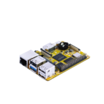
Development Kit (EM3568)

Hardware Design Guide
Peripheral Circuit Reference
External Power


Debug Circuit

USB OTG Interface Circuit

Note:
If common mode inductors are needed, it is recommended to keep 2.2ohm in series to improve the antistatic ability
PCB Footprint

Product Electrical Characteristics
Dissipation and Temperature
| Symbol | Parameter | Min | Typ | Max | Unit |
| VCC_SYS | System IOVoltage | 3.3V | 5 | 5.5 | V |
| Isys_in | VCC_SYSinput Current | 750 | mA | ||
| VCC3V3_SYS | System IOVoltage | 3.3-5% | 3.3 | 3.3+5% | V |
| Isys3v3_in | VCC_SYSinput Current | 500 | mA | ||
| VCC_RTC | RTC Voltage | 1.8 | 3 | 3.4 | V |
| Iirtc | RTC inputCurrent | 5 | 8 | uA | |
| Ta | Operating Temperature | -20 | 70 | °C | |
| Tstg | Storage Temperature | -40 | 85 | °C |
Reliability of Test
| High Temperature Operating Test | ||
| Contents | Operating 8h in high temperature | 55°C±2°C |
| Result | ||
| Operating Life Test | ||
| Contents | Operating in room | 120h |
| Result | ||
Documents / Resources
 |
Rockchip CM3568 Boardcon Embedded Design [pdf] User Manual CM3568 Boardcon Embedded Design, CM3568, Boardcon Embedded Design, Embedded Design, Design |