![]() UM12212
UM12212
S32K396-BGA-DC1
Rev. 1.0 — 3 February 2025
User manual
Document information
| Information | Content |
| Keywords | S32K396, EVB, User Manual |
| Abstract | Information necessary for work with S32K396-BGA EVB |
Introduction
This document describes the features of S32K396 289MapBGA Evaluation board (EVB). It provides guidance to developers about how the board should be utilized and describes its features.
The S32K396 MCU series includes S32K36x, S32K37x, and S32K39x. The S32K39 MCUs extend the highperformance capabilities of S32K37 with two programmable motor control co-processors and extended analogue capabilities. S32K396 is used throughout this document to cover all the variants of the MCU.
This S32K396 289MapBGA Daughter card (DC) is capable of operating standalone and can be extended by the S32X-MB Motherboard (MB) that is common also for S32Z/E family. MB provides another source of power supply for S32K396 MCU as well as extension of DC card functionality with more physical interfaces and user headers. Both boards are connected through the mating connectors (MB-DC).
S32K396 DC EVB overview
Daughter card is populated with several communication interfaces, user LEDs, push buttons, and headers (see Table 1). Several options for debug interfaces are enabled. JTAG is configured as a default debug interface.
Apart from that, the OpenSDA and Trace interfaces are enabled as well. DC card supports one Motor control interface and connector to attach EVB with Ethernet PHY. Three other options are also supported to deliver power supply for all the domains. EVB can be used standalone where power supply is provided from the 12V barrel connector and further provided by FS26 PMIC, or the supplies could be connected independently using the screw connector. In case of using MB to extend the functionality of the DC card, supply could be generated from MB on board regulators.

The daughtercard (DC) is capable of operating standalone and its functionality can be extended by the motherboard (MB). Both boards are connected through the mating connectors (MB-DC).
 Table 1. Overview of S32K396 EVB interfaces
| Interface | S32K396-BGA-DC1 | S32X-MB |
| CAN | 1x PHY (CAN0) | 4x PHY (CAN0, CAN1, CAN3, CAN4) |
| LIN | 2 x UART to LIN converter (UART2, UART3) | 2 x UART to LIN converter (UART2, UART3) |
| Ethernet | 1x connector (no PHY) | – |
| USB/UART | 2x (UART2, UART0) | 1x (UART 1) |
| MC connector | 1x | 1x |
| Zipwire | 1x | – |
| QSPI | 1x | – |
| MSC | 1x (headers – LPUART_MSC, DSPI) | – |
| I2C | 2x (1x USB-serial: I2C0, 1x header: I2C1) | – |
| FlexIO | Header | – |
| eMIOS | Header | – |
| User LED | 3x (PTD4, PTD5, PTH7) | 4x |
| User push button | 4x (PTE21,PTG0, PTG1, PTG2) | 4x |
| Potentiometer | – | 1x |
| BMS interface | 1 x header (J59, LPSPI2, LPSPI3) | – |
Start-up
3.1 PMIC mode configuration
FS26 supports two modes of operations, Normal and Debug, based on the jumper configuration (see Table 2 for the jumper configuration). When Normal mode is selected, FS26 watchdog is active and when it is not serviced in the timely manner, it issues reset to S32K396 by asserting the RESET_b signal. Based on the FS26 configuration after a couple of resets, the FS26 stops generating the MCU power supply.
Table 2. FS26 mode select
| FS26 mode | J10 | J11 |
| Normal | Open | Short |
| Debug (default) | Short | Open |
3.2 Power up
Follow these steps to power supply the board using an external 12V adapter:
- Following the ESD standard procedure when unpacking the S32K396-BGA-DC1.
- Make sure that the jumpers for power distribution and MCU power supply are configured correctly according to the intended power scheme.
- Configure J4 (5.0V), J7 (3.3V), and J6 (1.5 V) to get the power from the PMIC (position 2-4).
- Connect the necessary cables between the host PC and EVB prior to applying 12V power to the EVB.
- Apply the 12V power to EVB and flip the SW10 to ON position (right → left).
- When power is applied to the DC card, four green LEDs show the presence of the supply voltages as follows:
• LED D4 indicates that the 12.0V supply is connected to the DC correctly.
• LED D3 indicates that the VCC_5V0 supply is on.
• LED D2 indicates that the VCC_3V3 supply is on.
• LED D1 indicates that the 1.5V supply is on.

Power supply
There are three ways how the EVB can be supplied:
- External 12V/2A power supply
– FS26 PMIC generates all necessary power supplies:
– VCC_5V0 supply for analog and digital I/O (LDO2OUT)
– VCC_3V3 supply for digital I/O (LDO1OUT)
– 1.5 V supply to generate 1.1 V for core and logic (CORE)
– VREF – 5V supply for analog references (VREF) - External 5.0 V, 3.3 V, and 1.5 V power supplies over the screw type connectors [default]
- From the MB (12.0 V, 5.0 V, 3.3V, 1.5V)

4.1 EVB main 12 V power supply
Main supply for the daughtercard 12V can be supplied either from MB or DC supply connectors. To distribute the 12V power from either source further to the DC components, the SW10 must be in 1-2 position.
Table 3. DC 12V supply source selection
| Source of the 12V | J3 |
| DC card connectors, provided either from J1 or J2 | 1-2 (default) |
| Motherboard (through J55A) | 2-3 |
 VCC_12V is further used to supply VBAT_LIN and as a supply for Ethernet PHY Sabre board that can be connected through connector J53.
Note: SW10 has to be always in position 1-2 to enable 12V propagation to the DC card interfaces, also in the case that 12V is provided from the motherboard (J3 shorted in position 2-3).
Table 4. Main supply connector overview
| Connector | Reference | Description |
 |
DC: J1 | This connector should be used to connect the supplied wall-plug main adapter. Note: if a replacement or alternative adapter is used, you must ensure that the 2.1mm plug uses the correct polarization. |
 |
DC: J2 | This can be used to connect a bare wire lead to the EVB, typically from a laboratory power supply. The polarization of the connectors is clearly marked on the EVB. You must ensure correct connection. |
4.2 EVB VCC_5V0, VCC_3V3 power supply
There are three options for getting these power supplies on the daughtercard. See the following tables for details.
Table 5. DC VCC_5V0 supply configuration
| Source of VCC_5V0 | J4 | Note |
| External power screw connector (JP1 pin 4) | 1-2 (default) | Typically from a laboratory power supply. You must ensure correct connection, making sure GND is connected as well (JP1 pin 1 or 5). |
| MB through J56A | 2-3 | Ensure that J7 on MB is closed (1-2 short) |
| PMIC | 2-4 | – |
Table 6. DC VCC_3V3 supply configuration
| Source of VCC_3V3 | J7 | Note |
| External power screw connector (JP1 pin 3) | 1-2 (default) | Typically from a laboratory power supply. You must ensure correct connection, making sure GND is connected as well (JP1 pin 1 or 5). |
| MB through J56A | 2-3 | Ensure that J9 on MB is closed (1-2 short). |
| PMIC | 2-4 | – |
 4.3 EVB 1.5 power supply
There are four options for getting 1.5V supply on the daughtercard.
Table 7. DC 1.5V supply configuration
| 1.5V source | J6 | J26 | J28 | J29 | Note |
| External power screw connector (JP1 pin 2), typically from a laboratory power supply. | 1-2 (default) | Open (default) | 1-2 (default) | 2-3 (default) | You must ensure correct connection, making sure GND is connected as well (JP1 pin 1 or 5). Note that for this option, J26 must be left open and J28 must be configured to 1-2 short. |
| Buck converter on MB through J56A | 2-3 | Make sure that J68 on MB is closed (1-2 short) | |||
| PMIC | 2-4 | ||||
| Internal SMPS | Open | 1-2 | 2-3 | 1-2 (VDD_HV_ A)/2-3(VDD_HV_B) | J29 selects the source voltage for the SMPS |

4.4 1.1 V core power supply settings
Ensure that J27 is closed for 2-3 (default) for all the operating conditions. This connects the NMOS_CTRL signal to the gate of external NFET that regulates 1.1 V core and logic supply down from 1.5 V.
4.5 VDD_HV_A and VDD_HV_B
The VDD_HV_A and VDD_HV_B domains can be supplied either from VCC_5V0 or from VCC_3V3. The default and preferred configuration is to supply VDD_HV_A from VCC_5V0 and VDD_HV_B from VCC_3V3.
The VDD_HV_A configuration is ensured by soldered blob R6, which is by default, shorted to position 1-3 (VCC_5V0).
The VDD_HV_B configuration is ensured by soldered blob R334, which is by default, shorted to position 1-2 (VCC_3V3).
See the following table for the possible configuration of the VDD_HV_A and VDD_HV_B power supply domain and peripheral limitations.
Table 8. VDD_HV_A and VDD_HV_B configuration
| VDD_HV_A | VDD_HV_B | SDADC, ADCBIST, MSC, motor control (VDD_HV_A) | Ethernet, QSPI, Zipwire (VDD_HV_B) | ||
| Voltage | R6 | Voltage | R334 | ||
| VCC_5V0 | 1-3 (default) | VCC_3V3 | 1-2 (default) | Available | Available |
| VCC_5V0 | 1-3 | VCC_5V0 | 1-3 | Available | Not available |
| VCC_3V3 | 1-2 | VCC_3V3 | 1-2 | Not available | Available |
4.6 VDD_DCDC
The VDD_DCDC domain can be supplied either from VDD_HV_A or VDD_HV_B. The selection for VDD_DCDC supply is available by configuration of J29.
Note that J29 must not be left open, one of the supplies must be selected all the time.
 Table 9. VDD_DCDC supply configuration
| VDD_DCDC source | J29 |
| VDD_HV_A | 1-2 |
| VDD_HV_B | 2-3 (default) |
4.7 VDD_LVDS
The VDD_LVDS domain can be supplied only by the 3.3 V source. It can be connected either to VDD_HV_B or VCC_3V3. J30 provides options for supply source selection. When Zipwire is not used, then the VDD_LVDS power domain can be left unconnected.
Table 10. VDD_LVDS supply configuration
| VDD_LVDS power | J30 | Note |
| VCC_3V3 | 1-2 | – |
| VDD_HV_B | 2-3 (default) | Can be configured to this position only in case VDD_HV_B is supplied by 3.3 V |
| Unpowered | Open | Unpowered VDD_LVDS does not cause MCU reset (in this case, Zipwire cannot be used and VDD_ LVDS is signaled by flag in the PMC.LVSC register) |
4.8 VREFH
All voltage references of the MCU are connected to a single source, VREFH, which is recommended to be shorted with VDD_HV_A at the PCB level, or it can be supplied from PMIC. All VREFH_x pins must be supplied under all conditions and must not be left unconnected. Configuration is enabled by J63.
Table 11. VREFH source configuration
| VREFH source | J63 |
| PMIC VREF | 1-2 |
| VDD_HV_A | 2-3 (default) |

5.1 Reset, Wake, and LED indicator
On the DC card, there is a RESET switch (SW3) that provides a manual option to generate a reset signal to S32K396 MCU, which drives the RESET signal to reset the peripherals populated on the DC card. The RESET LED indicator (D15) is turned on (red light) when the RESET signal is active (J31 is closed).
The RESET_b signal is bidirectional and is routed to several interfaces on the DC card and to the MB through the MB_DC interface connectors (see the following table).
Table 12. RESET_b signal routing
| RESET_b connection | DC reference | Description |
| ETM Mictor Trace | J22 | When closed, RESET_b is routed to the ETM Mictor Trace connector. |
| Arm JTAG debug | J23 | When closed, RESET_b is routed to the Arm JTAG debug connector. |
| FS26 | J12 | When closed, RESET_b is routed to FS26. |
| Reset push button | J31 | When closed, RESET_b is routed to SW3. |
| QSPI | J36 | When closed, RESET_b is routed to the external QSPI memory. |
| Ethernet | J60 | When closed, RESET_b is routed to external both Sabre connector and also Ethernet PHY on the MB. |
| USB/Serial | J67 | When closed, RESET_b is routed from the USB/ Serial interface controlled GPIO to the MCU. |
For the purpose of external wake-up source, the SW4 is routed to PTB19 that implements wake-up input functionality WKPU[38]. This is one of the ways to get the MCU wake-up from Standby mode.
5.2 Debug interface
On the DC card, there are three possible options for debugging sharing of the same signals. Signal routing for the particular debug interfaces are selectable by jumpers J16, J17, J18, and J19. See the description of configuration in the three options.
Table 13. Debug interface selection
| Debug interface | J16, J17, J18, J19 |
| Arm JTAG | 2-4 (default) |
| Mictor Trace | 2-3 |
| OpenSDA | 1-2 |
Table 14. DC card Debug interfaces overview
| Connector | DC reference | Description | |
| 20-pin Arm standard JTAG connector |
|
J20 | It supports the JTAG interface for accessing ARM7 and ARM9 based devices. For Cortex- Mx devices, it supports Serial Wire and JTAG interfaces for accessing all SWD, SWV, and JTAG signals available on a Cortex-Mx device. |
| 38-pin Arm ETM Mictor Connector |
|
P1 | The Mictor (Matched Impedance Connector) has been the standard way to connect a trace probe to an Arm target. Cortex-M7 supports 16-bit data trace using the Mictor connector. This is only available with DS-5 using a DSTREAM debug and trace unit. |
| OpenSDA |
|
J15 | Micro USB connector is used to connect to the onboard OpenSDA debug interface that bridges serial and debug communication between a USB host and the embedded target processor. The debug circuit is based on Kinetis MK65 MCU. |


USB interface
On the DC card, LPUART0 is routed to the OpenSDA debug interface (J15) that supports also passing the USB to serial communication.
There is also MCP2221 (U32) interface for USB to UART/I2C conversion with GPIO functionality. It uses J64 USB-B type connector and it is connected to LPI2C0 instance and LPUART2 instance.
Table 15. USB to serial interfaces on DC
| Interface | DC reference | Signal name | MCU port |
Description |
|
| OpenSDA
|
J15 | LPUART0_RX | PTE10 | UART Receive | |
| LPUART0_TX | PTE11 | UART Transmit | |||
| USB/serial
|
J64
|
LPUART2_RX | PTH9 | UART Receive | |
| LPUART2_TX | PTH8 | UART Transmit | |||
| LPI2C0_SDA | PTF21 | LPI2C Data I/O | |||
| LPI2C0_SCL | PTF20 | LPI2C Clock I/O | |||
| USB_RESET | RESET_B | When the J67 is populated, it can control the Reset signal | |||

LIN interface
On the S32K396 DC is populated TJA1022 dual LIN transceiver capable to operate in both Master and Slave modes (jumper selectable: J50 and J51) and its outputs are connected to LIN interface connector J52. The MCU communicates with the driver over LPUART.
 Table 16. LIN PHY configuration
| LIN PHY | Jumper position | Configuration |
| 1 (J50) | Open (default) | Slave |
| close | Master | |
| 2 (J51) | Open (default) | Slave |
| Close | Master |
Pinout of the LIN header is detailed in the following table.
Table 17. LIN interface connector J52
| Pin number | Signal |
| 1 | GND |
| 2 | GND |
| 3 | NC |
| 4 | NC |
| 5 | VBAT_LIN |
| 6 | VBAT_LIN |
| 7 | LIN2 |
| 8 | LIN1 |
The list of signals connected from MCU to LIN transceiver is provided in the following table. MCU signals for LIN1 are from the VDD_HV_A supply domain and signals for LIN2 from are from the VDD_HV_B domain.
Table 18. LIN connection from MCU to DC card LIN transceiver
| LIN interface | MCU Signal name | MCU port |
| 1 | LPUART3_RX | PTC20 |
| LPUART3_TX | PTE1 |
| LIN interface | MCU Signal name | MCU port |
| 2 | LPUART2_RX | PTC12 |
| LPUART2_TX | PTC13 |
CAN interface
8.1 CAN interface on Daughtercard (DC)
On the S32K396 DC1 card is populated one CAN transceiver TJA1044GT. The CAN signals are routed on header J34 and are from the VDD_5V0 supply domain. The Standby mode for the PHY can be controlled by the J35 (Standby: 1-2; Normal (default): 2-3).
 Table 19. CAN connection from MCU to DC card CAN transceiver
| Signal name | MCU port | Description | Note | |
| CAN0_TX | PTC21 | CAN Tx channel | ||
| CAN0_RX | PTC23 | CAN Rx channel |
Ethernet interface
On the S32K396 EVB card, there is no Ethernet PHY but the Ethernet interface providing MII and/or RMII signals are routed to Sabre connector J53. Ethernet PHY Sabre expansion board can be plugged in there and used.
Table 20. Configuration of the Ethernet signals for the PHY interface on DC and MB
| Signal | Configuration resistors on DC | DC SABRE interface enable: resistor configuration | MB TJA1103A PHY enable: resistor configuration |
| EMAC_MII_RMII_MDC | R521 | DNP | Populated |
| EMAC_MII_RMII_MDIO | R530 | DNP | Populated |
| EMAC_MII_RMII_TX_EN | R532 | DNP | Populated |
| EMAC_MII_RMII_RX_ER | R522 | DNP | Populated |
| EMAC_MII_CRS | J61 | Open | J61 short 2-3 |
| EMAC_MII_RXD3 | R529 | DNP | Populated |
| EMAC_MII_RMII_RXD[0] | R519 | DNP | Populated |
| EMAC_MII_RMII_RXD[1] | R528 | DNP | Populated |
| EMAC_MII_RXD2 | R520 | DNP | Populated |
| EMAC_MII_TXD3 | R534 | DNP | Populated |
| EMAC_MII_TXD2 | R538 | DNP | Populated |
| EMAC_MII_RMII_TXD[1] | R533 | DNP | Populated |
| EMAC_MII_RMII_TXD[0] | R537 | DNP | Populated |
| EMAC_MII_RMII_TX_CLK | R536 | DNP | Populated |
| EMAC_MII_RX_CLK | R539 | DNP | Populated |
| EMAC_MII_RMII_RX_DV | J61 | Open | J61 short 1-2 |
The following figure depicts the SABRE interface J53 to connect TJA1103SDB SABRE development board.
Make sure resistors R266, R519, R520, R521, R522, R528, R529, R530, R532, R533, R534, R536, R537, R538, R539 are DNP and J61 is open to use the TJA1103SDB SABRE development board.
Table 21. Ethernet signals routed to the Sabre interface connector in DC
| Signal | MCU port | Description |
| EMAC_MII_RMII_MDC | PTD17 | ENET clock for control data transfer to PHY |
| EMAC_MII_RMII_MDIO | PTD16 | ENET control data to/from PHY |
| EMAC_MII_RMII_TX_EN | PTE9 | ENET transmit enable |
| EMAC_MII_RMII_RX_ER | PTC16 | ENET receive error |
| EMAC_MII_COL | PTB27 | ENET MII collision detected |
| EMAC_MII_RXD3 | PTC15 | ENET receive data (MII mode only) |
| EMAC_MII_RMII_RXD[0] | PTB23 | ENET receive data |
| EMAC_MII_RMII_RXD[1] | PTB24 | ENET receive data |
| EMAC_MII_RXD2 | PTC14 | ENET receive data (MII mode only) |
| EMAC_MII_TXD3 | PTB3 | ENET transmit data (MII mode only) |
| EMAC_MII_TXD2 | PTB28 | ENET transmit data (MII mode only) |
| EMAC_MII_RMII_TXD[1] | PTB29 | ENET transmit data |
| EMAC_MII_RMII_TXD[0] | PTC18 | ENET transmit data |
| EMAC_MII_RMII_TX_CLK | PTC19 | ENET transmit clock |
| EMAC_MII_RX_CLK | PTB26 | ENET MII receive clock |
| EMAC_PPS1 | PTD13 | ENET 1588 timer channel |
| EMAC_PPS0 | PTA26 | ENET 1588 timer channel |
| EMAC_MII_CRS | PTB22 | ENET MII carrier sense |
| EMAC_MII_RMII_RX_DV | PTD14 | ENET receive data valid |
Note Those signals are dedicated to the Ethernet interface and are routed to the Sabre connector.
QSPI interface
On the DC card there is populated S71KL512SC0 3.0V 512 Mb HyperFlash and 64Mb HyperRAM in multichip package. Selection of the target memory is done by the corresponding chip select signal. The memory is connected to the QSPI interface of the S32K396 MCU that features only one chip select, so the selection is done by soldered resistor R328 (1-2 by default, selecting Hyper Flash).
Table 22. QSPI memory chip select configuration
| Selected memory | R328 | Description |
| Hyper Flash | 1-2 (default) | QSPI_PCSFA is connected to CS1 pin of external memory |
| Hyper RAM | 2-3 | QSPI_PCSFA is connected to CS2 pin of external memory |
There is a level shifter used only for the RESET_b signal because this pin is supplied from the VDD_HV_A domain. The reset signal can be disconnected from QSPI memory by header J36 (default close).
Warning
QSPI interface is supplied from the VDD_HV_B domain, so the QSPI memory can only be used when VDD_HV_B is supplied from VCC_3.0V (default configuration). In case VDD_HV_B is reconfigured to be supplied from VCC_5.0V, then zero ohm resistors (see below table) connecting the QSPI signals from MCU to memory have to be removed.
Table 23. QSPI signal overview
| MCU port | Signal name | Serial resistor | Description |
| PTD11 | QuadSPI_IOFA0 | R316 | QuadSPI serial data for serial flash device A (fast) |
| PTD7 | QuadSPI_IOFA1 | R322 | QuadSPI serial data for serial flash device A (fast) |
| PTD12 | QuadSPI_IOFA2 | R317 | QuadSPI serial data for serial flash device A (fast) |
| PTC2 | QuadSPI_IOFA3 | R318 | QuadSPI serial data for serial flash device A (fast) |
| PTC0 | QuadSPI_IOFA4 | R319 | QuadSPI serial data for serial flash device A (fast) |
| PTD9 | QuadSPI_IOFA5 | R324 | QuadSPI serial data for serial flash device A (fast) |
| PTD8 | QuadSPI_IOFA6 | R320 | QuadSPI serial data for serial flash device A (fast) |
| PTC17 | QuadSPI_IOFA7 | R321 | QuadSPI serial data for serial flash device A (fast) |
| PTD10 | QuadSPI_SCKFA | R326 | QuadSPI serial clock for serial flash device A (fast) |
| PTC1 | QuadSPI_DQSFA | R325 | QuadSPI data strobe signal Flash A (RWDS) |
| PTC3 | QuadSPI_PCSFA | R327 | QuadSPI chip select for serial flash device A |
Zipwire
There is the Zipwire interface connector populated on the DC card. The connector type is Samtec (ERF8-005-05.0-L-DV-L-TR). There are also populated handy testpoints on Zipwire signals that are useful for debugging and performance evaluation.
 The following table describes the connector.
Table 24. Zipwire interface connector description
| Connector | Tag | Pin number | Signal |
 |
J41 | 1 | TX_P |
| 2 | GND | ||
| 3 | TX_N | ||
| 4 | GND | ||
| 5 | GND | ||
| 6 | REF_CLK | ||
| 7 | RX_N | ||
| 8 | GND | ||
| 9 | RX_P | ||
| 10 | GND | ||
| 11 | GND | ||
| 12 | GND |
Signal connection to the Zipwire interface from MCU is listed in the following table.
Table 25. Zipwire interface connection to MCU
| Zipwire interface | Signal name | MCU port/pin | Description |
| RX_N | LFAST_0_RxD_N | – | LVDS receive negative terminal |
| RX_P | LFAST_0_RxD_P | – | LVDS receive positive terminal |
| TX_N | LFAST_0_TxD_N | – | LVDS transmit negative terminal |
| TX_P | LFAST_0_TxD_P | – | LVDS transmit positive terminal |
| REF_CLK | LFAST_0_EXT_REF_I/O | PTA29 | LFAST reference clock input/output |
Testpoints where LFAST signals can be accessed are listed in the following table.
Table 26. Test points for LFAST signals
| Test point | Signal name |
| TP45 | LFAST_0_RxD_N |
| TP48 | LFAST_0_RxD_P |
| TP47 | LFAST_0_TxD_N |
| TP44 | LFAST_0_TxD_P |
| TP46 | LFAST_0_EXT_REF_I/O |
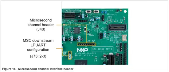
Microsecond channel
The microsecond channel (MSC) communication interface is composed of two IPs. It uses the DSPI interface with LVDS signals (data and clock signals) for upstream channel and the UART interface (only UART Rx channel) for the downstream channel. Chip select signals and UART RX are single-ended signals. Microsecond channels are available on the header J40. For using the microsecond channel, the J73 needs to be populated to position 2-3. -3 (default 1-2 to power SBC)
Table 27. Microsecond channel interface signal overview
| Signal | MCU port/pad | Description | Note |
| DSPI_MSC0_SCK_N | -/U16 | LVDS MSC output clock negative terminal | Dedicated LVDS pads, not multiplexed with any other functionality. Can be used only when VDD_HV_A is supplied from VCC_5V0 because these pins are powered by the VDD_HV_A. |
| DSPI_MSC0_SCK_P | -/U15 | LVDS MSC output clock positive terminal | |
| DSPI_MSC0_SOUT_N | -/T14 | LVDS MSC data output negative terminal | |
| DSPI_MSC0_SOUT_P | -/U13 | LVDS MSC data output positive terminal | |
| DSPI_MSC0_PCS[0] | PTF14/F15 | DSPI MSC peripheral chip select 0 | – |
| DSPI_MSC0_PCS[1] | PTF15/F14 | DSPI MSC peripheral chip select 1 | – |
| LPUART_MSC0_RX | PTF26/R12 | Downstream UART Rx channel | – |
Table 28. J73 configuration
| Functionality of PTF26 | J73 |
| LPSPI communication with FS26 | 1-2 (default) |
| MSC LPUART downstream channel | 2-3 |
Motor control interface
There is one motor control interface connector populated on the DC (see Table 31 for detailed signal description and assignment). Motor control interface is available only when VDD_HV_A is using VDD_5V0. This interface is compatible with low-voltage (GD33937) and high-voltage (GD3162) gate driver boards. The following table describes the functionality of each pin. Because the high voltage gate driver board has a bit different functionality, the differences are listed in a bold format in the table.
Caution
It is necessary to select excitation signal for the resolver by the J45.
Table 29. Motor control interface connections on DC
| Motor control interface | ||||||||
| MCU/board routing | Function | Name | Pin | Name | Function | MCU/board routing | ||
| VCC_5V0 | Analog reference supply | VREF | B1 | A1 | VDDA | Analog power supply | VDD_5V0 | |
| AGND | Analog ground | GNDA2 | B2 | A2 | GNDA1 | Analog ground | AGND | |
| PTE18 | DC bus current | A0 | B3 | A3 | A1 | Phs. U current | PTD1 | |
| PTA8 | DC bus voltage | A2 | B4 | A4 | A3 | Phs. V current | PTE26 | |
| NC | Analog input | A4 | B5 | A5 | A5 | Phs. W current | PTA24 | |
| NC | Analog input | A6 | B6 | A6 | A7 | Analog input | NC | |
| NC | Analog input | A8 | B7 | A7 | A9 | Analog input | NC | |
| PTE6 | Resolver sine negative differential | A10 | B8 | A8 | A11 | Resolver sine single ended/diff positive | PTE2 | |
| PTE17 | Resolver cos negative differential | A12 | B9 | A9 | A13 | Resolver cos single ended/diff positive | PTA16 | |
| NC | – | 14 | B10 | A10 | A15 | Analog input/ EXC_SIG_DEN | NC | |
| AGND | Analog ground | GNDA3 | B11 | A11 | GNDA4 | Analog ground | AGND | |
| VDD_HV_A | Digital power supply MC | U_VCC | B12 | A12 | VCC_PER | Digital power supply | VDD_HV_A | |
| GND | Digital ground | GND1 | B13 | A13 | GND2 | Digital ground | GND | |
| PTF0 | U_Transistor_ Temp_H/Encoder_A | TM0 | B14 | A14 | PWM0 | PWM Phs U H | PTD24 | |
| PTF9 | U_Transistor_ Temp_L/Encoder_B | TM1 | B15 | A15 | PWM1 | PWM Phs U L | PTA2 | |
| PTF4 | V_Transistor_Temp_ L/Encoder_Index | TM2 | B16 | A16 | PWM2 | PWM Phs V H | PTA3 | |
| PTF5 | V_Transistor_ Temp_H | TM3 | B17 | A17 | PWM3 | PWM Phs V L | PTD23 | |
| PTE27 | W_Transistor_ Temp_L | TM4 | B18 | A18 | PWM4 | PWM Phs W H | PTD2 | |
| PTB12/SWG0 | Resolver excitation | TM5 | B19 | A19 | PWM5 | PWM Phs W L | PTD3 | |
| PTF14 | Run button | IO1 | B20 | A20 | PWM6 | U_GS discharge | PTE19 | |
| PTA20 | SPI_MISO | MISO | B21 | A21 | PWM7 | U_GS Charge/ Brake PWM | PTB2 | |
| PTA18 | SPI_MOSI | MOSI | B22 | A22 | PWM8 | V_GS Discharge/ Zero Cross Phase U | PTA30 | |
| PTA19 | SPI_SCK | SCKL | B23 | A23 | PWM9 | V_GS Charge/Zero cross Phase V | PTB18 | |
| PTA21 | SPI CS Low/SPI CS | /SS | B24 | A24 | PWM10 | W_GS Discharge/ Zero cross Phase W | PTB21 | |
| PTA17 | W_Transistor_ Temp_H | IO2 | B25 | A25 | PWM11 | W_GS Charge | PTA31 | |
| PTG3 | W_Transistor_ turnon_check_ H/UART TXD | SCI_TXD | B26 | A26 | FAULT1 | INTB_HS/Fault_OC | PTB15 | |
| PTG8 | W_Transistor_ turnon_check_ L/UART RXD | SCI_RXD | B27 | A27 | FAULT2 | INTB_LS/Fault_OV | PTB16 | |
| PTA14 | Fail safe enable/ GD enable | IO3 | B28 | A28 | FAULT3 | U_Transistor_ turnon_check_H | PTD20 | |
| PTA23 | Fail state low side/GD Reset | IO4 | B29 | A29 | FAULT4 | U_Transistor_ turnon_check_L | PTB17 | |
| PTG4 | Fail state high side/GD INT | IO5 | B30 | A30 | IO6 | SPI CS High | PTA22 | |
| VCC_12V | 12V power supply | VPOWER | B31 | A31 | IO7 | V_Transistor_ turnon_check_ H/SW_UP | PTB5 | |
| GND | Digital GND/ Power GND | GNDP | B32 | A32 | IO8 | V_Transistor_ turnon_check_ L/SW_Down | PTB13 | |
Table 30. Resolver excitation signal selection
| Source of the resolver excitation signal | J45 |
| Sine Wave Generator 0 | 1-2 |
| eTPU_B_CH[2]/eTPU_A_[0]/GPIO pin | 2-3 |

User interface
There are several pin headers where multiple signals are available as well as three user LEDs and four push buttons.
Table 31. User interface summary
| Module | DC reference | Description |
| I2C | J39 | LPI2C1 interface |
| FlexIO | J62 | 32 signals of FlexIO accessible on the header |
| eMIOS0 | J58 | 8 signals of eMIOS accessible on headers |
| User LED | D35 | PTH7 MCU port configured as GPIO |
| D34 | PTD4 MCU port configured as GPIO | |
| D33 | PTD5 MCU port configured as GPIO | |
| User push buttons | SW5 | PTE21 MCU port configured as GPIO. J71 needs to be shorted to position 2-3 to select the SW5 functionality. |
| SW7 | PTG2 MCU port configured as GPIO | |
| SW8 | PTG1 MCU port configured as GPIO | |
| SW9 | PTG0 MCU port configured as GPIO |

Battery management interface
There are populated MC33664ATL1EG isolated network high-speed transceivers for communication with the battery subsystem. The MCU communicates with the device through two LPSPI interfaces (LPSPI2 – master, LPSPI3 – slave) and two GPIO pins. The battery management (BMS) interface is using the header J59.
Table 32. BMS interface signal overview
| Module | Functionality | MCU port | Description |
| LPSPI2 | SCK | PTF0 | Upstream communication |
| PCS0 | PTF3 | ||
| SOUT | PTF2 | ||
| GPIO | EN | PTH11 | Control the BMS device mode (Normal/Sleep) |
| LPSI3 | SCK | PTF13 | Downstream communication |
| PCS0 | PTF16 | ||
| SIN | PTF12 | ||
| GPIO | INT | PTH12 | BMS interrupt to trigger the device wake up |
Monitoring of the internal signal
The TRGMUX_APP module includes the possibility to monitor the internal triggers over the pins. On the EVB is accessible 9 from 16 TRGMUX outputs as shown in the following table.
To route the internal signals to the pins, the following needs to be configured:
- Output functionality of the pin as TRGMUX output in the SIUL2 module (SIUL2.MSCR[x].B.SSS)
- Output buffer enabled in the SIUL2 module (SIUL2.MSCR[x].B.OBE)
- Selected signal needs to be configured in the TRGMUX_AP module based on the selection done based on the S32K39_and_S32K37_TRMUX_connectivity.xlsx/S32K36_TRMUX_connectivity.xlsx spread sheet attached to the RM Also the eTPU signals can be routed over the TRGMUX_APP on the pins but for that you need to route them to the TRGMUX_APP (signals TRGMUX_MSC_TRGMUX_IN0 – TRGMUX_MSC_TRGMUX_IN9) by configuring TRGMUX_MSC (registers TRGMUX_APP_TRGMUX_OUT0 – TRGMUX_APP_TRGMUX_OUT9)
- TRGMUX_APP number of input signals are limited to 128 and for expanding them, the monitor mux functionality is used that routes additional internal signals to the TRGMUX_APP to the inputs 2, 3, and 4 by configuring the monitor mux registers place in the SIUL2 module (MUX0_TIMER_EN1, MUX0_BCTU1_EN, MUX1_TIMER_EN0, MUX1_BCTU0_EN, MUX1_MISC_EN, MUX2_TIMER_EN1, MUX2_BCTU1_EN, MUX2_MISC_EN). These signals are listed in the Monitor Mux sheet of the spreadsheet mentioned above. If you want to have one internal signal on the TRGMUX_APP input, you need to set only one bit in the specific MUX register because these signals are ORed before entering the TRGMUX_APP input.
Table 33. TRGMUX_OP output signal summary
| TRGMUX_OUTPUT | Port pin | Board routing | MSCR | MSCR[SSS] | TRGMUX_ APP register | TRGMUX_APP register SEL bitfield number |
| 0 | PTE5 | J62.8 | 133 | 0x8 | SIUL_ OUT_0 (32) | 0 |
| 1 | PTD0 | TP95 | 96 | 0x7 | 1 | |
| 4 | PTE10 | TP90 | 138 | 0x7 | SIUL_ OUT_1 (33) | 0 |
| 5 | PTE11 | TP88 | 139 | 0x7 | 1 | |
| 8 | PTA31 | J44.A25 | 31 | 0x7 | SIUL_ OUT_2 (34) | 0 |
| 9 | PTB18 | J44.A23 | 50 | 0x7 | 1 | |
| 10 | PTB19 | J32.2 | 51 | 0x7 | 2 | |
| 12 | PTB21 | J44.A24 | 53 | 0x7 | SIUL_ OUT_3 (35) | 0 |
| 13 | PTB22 | J61.3 | 54 | 0x7 | 1 |

Default jumper configuration
Table 34. Default jumper configuration
| Module | Functionality | DCreference | Default connection | Description |
| Input power distribution | VCC_12V | J3 | 1-2 | Main supply is sourced from DC card connectors, provided either from J1 or J2. |
| VCC_5V0 | J4 | 1-2 | Supplied from external power screw connector (JP1 pin 4). | |
| VCC_1V5 | J6 | 1-2 | Supplied from external power screw connector (JP1 pin 2). | |
| VCC_3V3 | J7 | 1-2 | Supplied from external power screw connector (JP1 pin 3). | |
| VDD_HV_B | R334 | 1-2 | Supplied from VCC_3V3. | |
| VDD_HV_A | R6 | 1-3 | Supplied from VCC_5V0. | |
| FS26 PMI
|
Debug mode | J10 | Closed | Debug pin is connected to positive voltage to enable Debug mode. |
| J11 | Open | Left open when configuring FS26 for a debug mode. | ||
| Reset/Wake | J12 | Closed | RESET_b signal connected to WAKE2 and RSTB pins of FS26. | |
| SPI interface | J71 | 1-2 | PTE21 routed to FS26 as SIN | |
| J73 | 1-2 | PTF26 routed to FS26 as PCS1 | ||
| J75 | 2-3 | PTC11 routed to FS26 as SOUT | ||
| Debug | Select the interface | J16 | 2-4 | Arm JTAG connector selected for TDI signal. |
| J17 | 2-4 | Arm JTAG connector selected for TMS signal. | ||
| J18 | 2-4 | Arm JTAG connector selected for TCK signal. | ||
| J19 | 2-4 | ARM JTAG connector selected for TDO signal. | ||
| Power | J21 | Closed | VDD_HV_A connected to pin 2 of Arm JTAG debug connector. | |
| Reset | J22 | Closed | RESET_b signal connected to Arm ETM Mictor trace connector. | |
| J23 | Closed | RESET_b signal connected to Arm JTAG debug connector. | ||
| J68 | Open | Keep this jumper open | ||
| MCU power
|
VDD_1V5 | J26 | Open | Sourced from external source, not from MCU internal SMPS. |
| NMOS gate control | J27 | 2-3 | NMOS_CTRL signal from MCU connected to the gate of external NFET to regulate 1.1V core and logic supply down from 1.5V. | |
| PMOS gate control | J28 | 1-2 | Gate of the P-MOS is shorted to the VDD_DCDC. PMOS_CTRL is left open. | |
| VDD_DCDC | J29 | 2-3 | Sourced from VDD_HV_B. | |
| VDD_LVDS | J30 | 2-3 | Sourced from VDD_HV_B. |
Abbreviations
MCU – Microcontroller Unit
EVB – Evaluation Board
DC – Daughter Card
MB – Motherboard card
PMIC – Power Management Integrated Circuit
ESD – Electrostatic Discharge
PHY – Physical interface
SMPS – Switched-Mode Power Supply
USB – Universal Serial Bus
MSC – Microsecond Channel
BMS – Battery Management System
Revision history
Revision history
| Document ID | Release date | Description |
| UM12212 v.1.0 | 03 February 2025 | Initial release |
Legal information
Definitions
Draft — A draft status on a document indicates that the content is still under internal review and subject to formal approval, which may result in modifications or additions. NXP Semiconductors does not give any representations or warranties as to the accuracy or completeness of information included in a draft version of a document and shall have no liability for the consequences of use of such information.
Disclaimers
Limited warranty and liability — Information in this document is believed to be accurate and reliable. However, NXP Semiconductors does not give any representations or warranties, expressed or implied, as to the accuracy or completeness of such information and shall have no liability for the consequences of use of such information. NXP Semiconductors takes no responsibility for the content in this document if provided by an information source outside of NXP Semiconductors. In no event shall NXP Semiconductors be liable for any indirect, incidental, punitive, special or consequential damages (including – without limitation lost profits, lost savings, business interruption, costs related to the removal or replacement of any products or rework charges) whether or not such damages are based on tort (including negligence), warranty, breach of contract or any other legal theory.
Notwithstanding any damages that customer might incur for any reason whatsoever, NXP Semiconductors’ aggregate and cumulative liability towards customer for the products described herein shall be limited in accordance with the Terms and conditions of commercial sale of NXP Semiconductors.
Right to make changes — NXP Semiconductors reserves the right to make changes to information published in this document, including without limitation specifications and product descriptions, at any time and without notice. This document supersedes and replaces all information supplied prior to the publication hereof. Applications — Applications that are described herein for any of these products are for illustrative purposes only. NXP Semiconductors makes no representation or warranty that such applications will be suitable for the specified use without further testing or modification.
Customers are responsible for the design and operation of their applications and products using NXP Semiconductors products, and NXP Semiconductors accepts no liability for any assistance with applications or customer product design. It is customer’s sole responsibility to determine whether the NXP Semiconductors product is suitable and fit for the customer’s applications and products planned, as well as for the planned application and use of customer’s third party customer(s). Customers should provide appropriate design and operating safeguards to minimize the risks associated with their applications and products.
NXP Semiconductors does not accept any liability related to any default, damage, costs or problem which is based on any weakness or default in the customer’s applications or products, or the application or use by customer’s third party customer(s). Customer is responsible for doing all necessary testing for the customer’s applications and products using NXP Semiconductors products in order to avoid a default of the applications and the products or of the application or use by customer’s third party customer(s). NXP does not accept any liability in this respect.
Terms and conditions of commercial sale — NXP Semiconductors products are sold subject to the general terms and conditions of commercial sale, as published at https://www.nxp.com/profile/terms, unless otherwise agreed in a valid written individual agreement. In case an individual agreement is concluded only the terms and conditions of the respective agreement shall apply. NXP Semiconductors hereby expressly objects to applying the customer’s general terms and conditions with regard to the purchase of NXP Semiconductors products by customer.
Suitability for use in automotive applications — This NXP product has been qualified for use in automotive applications. If this product is used by customer in the development of, or for incorporation into, products or services (a) used in safety critical applications or (b) in which failure could lead to death, personal injury, or severe physical or environmental damage (such products and services hereinafter referred to as “Critical Applications”), then customer makes the ultimate design decisions regarding its products and is solely responsible for compliance with all legal, regulatory, safety, and security related requirements concerning its products, regardless of any information or support that may be provided by NXP. As such, customer assumes all risk related to use of any products in Critical Applications and NXP and its suppliers shall not be liable for any such use by customer.
Accordingly, customer will indemnify and hold NXP harmless from any claims, liabilities, damages and associated costs and expenses (including attorneys’ fees) that NXP may incur related to customer’s incorporation of any product in a Critical Application.
Export control — This document as well as the item(s) described herein may be subject to export control regulations. Export might require a prior authorization from competent authorities.
HTML publications — An HTML version, if available, of this document is provided as a courtesy. Definitive information is contained in the applicable document in PDF format. If there is a discrepancy between the HTML document and the PDF document, the PDF document has priority.
Translations — A non-English (translated) version of a document, including the legal information in that document, is for reference only. The English version shall prevail in case of any discrepancy between the translated and English versions.
Security — Customer understands that all NXP products may be subject to unidentified vulnerabilities or may support established security standards or specifications with known limitations. Customer is responsible for the design and operation of its applications and products throughout their lifecycles to reduce the effect of these vulnerabilities on customer’s applications and products. Customer’s responsibility also extends to other open and/or proprietary technologies supported by NXP products for use in customer’s applications. NXP accepts no liability for any vulnerability. Customer should regularly check security updates from NXP and follow up appropriately.
Customer shall select products with security features that best meet rules, regulations, and standards of the intended application and make the ultimate design decisions regarding its products and is solely responsible for compliance with all legal, regulatory, and security related requirements concerning its products, regardless of any information or support that may be provided by NXP.
NXP has a Product Security Incident Response Team (PSIRT) (reachable at PSIRT@nxp.com) that manages the investigation, reporting, and solution release to security vulnerabilities of NXP products.
NXP B.V. — NXP B.V. is not an operating company and it does not distribute or sell products.
Trademarks
Notice: All referenced brands, product names, service names, and trademarks are the property of their respective owners.
NXP — wordmark and logo are trademarks of NXP B.V.
AMBA, Arm, Arm7, Arm7TDMI, Arm9, Arm11, Artisan, big.LITTLE, Corpyrights, designs and trade secrets. All rights reserved.
Kinetis — is a trademark of NXP B.V.
Please be aware that important notices concerning this document and the product(s) described herein, have been included in section ‘Legal information’.
© 2025 NXP B.V.
For more information, please visit: https://www.nxp.com
All rights reserved.
Document feedback
Date of release: 3 February 2025
Document identifier: UM12212
Documents / Resources
 |
NXP S32K396 Motor Control Development Kit [pdf] User Manual S32K396-BGA-DC1, S32K396 289MapBGA, S32K396 Motor Control Development Kit, S32K396, Motor Control Development Kit, Control Development Kit, Development Kit |