GEXUN 20800D8-04V1.0 and 1ANT IEEE 802. 11 Wi-Fi Integrated Module

Introduction
20800D8-04 module is based on AIC8800D40 solution. 20800D8-04 is a combo low-power, high-performance and high-integrated dual band wireless communication module which is designed for meeting the customers ’needs of small size and low cost. This module supports both WLAN and functions. Its WLAN/function supports the USB2.0/SDIO3.0 interface, and its BT function supports the UART interface, and the module meets the requirements of standard protocol IEEE 802.11 . Such units as power management, power amplifier and low- noise amplifier are integrated in the main chip of the module. Its WLAN PHY rate is up to 2 8 6 . 8 Mbps@TX. The module can be applied in smart sound boxes, set- top boxes,game machines, printers, IP cameras, tachographs, and other smart equipment. This documentation describes the engineering requirements specification.
Features
| Reserving System | |
| IEEE Std. 802.11b | |
| IEEE Std. 802.11g | |
| IEEE Std. 802.11n | |
| IEEE Std. 802.11ax | |
| Chip Solution | AIC8800D40 |
| Band | 2.4GHz |
| Dimensions | 12mm×12mm×1.85mm |
| Antenna | Stamp Hole |
| Installation Mode | SMD |
| Remark |
Block Diagram

Package Outline and Mounting

Pin Definition
|
|
||
| PIN | SYMBOL | DESCRIPTION |
| 1 | GND | Connected to Ground |
| 2 | WL_ANT | 2.4 |
| 3 | GND | Connected to Ground |
| 4 | NC | – |
| 5 | NC | – |
| 6 | GPIOB5/HOST_WAKE | |
| 7 | GPIOB3/WAKE_HOST | |
| 8 | NC | – |
| 9 | VBAT | 3.3V |
| 10 | NC | |
| 11 | NC | – |
| 12 | PWR_WF | PWR_KEY |
| 13 | WL_WAKE_HOST | WIFI |
| 14 | SDIO_D2 | I/O |
| 15 | SDIO_D3 | I/O |
| 16 | SDIO_CMD | I/O |
| 17 | SDIO_CLK | I/O |
| 18 | SDIO_D0 | I/O |
| 19 | SDIO_D1 | I/O |
| 20 | GND | Connected to Ground |
| 21 | NC | – |
| 22 | VIO | 3.3V/1.8V |
| 23 | NC | – |
| 24 | NC | – |
| 25 | PCM_OUT | I/O |
| 26 | PCM_CLK | I/O |
| 27 | PCM_IN | I/O |

| 28 | PCM_SYNC | I/O |
| 29 | UART0_TX | I/O |
| 30 | UART0_RX | I/O |
| 31 | GND | Connected to Ground |
| 32 | NC | – |
| 33 | GND | Connected to Ground |
| 34 | PWR_ | GPIO/_DIS |
| 35 | NC | GPIO |
| 36 | GND | Connected to Ground |
| 37 | NC | – |
| 38 | NC | – |
| 39 | NC | – |
| 40 | NC | – |
| 41 | UART1_RTS | I/O |
| 42 | UART1_TX | I/O |
| 43 | UART1_RX | I/O |
| 44 | UART1_CTS | I/O |
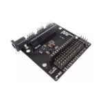
P|roduct Pictures

Key Materials
| 1 | AIC8800D40 | QFN48 | AIC | |
| 2 | PCB | |||
| 3 | ||||
| 4 |
General Requirements
| No. | Feature | Description |
| 8-1 | Operation Voltage | 3.3V±0.3 |
| 8-2 | Current Consumption | 580mA |
| 8-3 | Ripple | ≤120mV |
| 8-4 | Operation Temperature | -20°C to +40°C |
| 8-5 | Antenna Type | External antenna |
| 8-6 | Interface | SDIO3.0/USB2.0/PCM/UART |
| 8-7 | Storage Temperature | -40°C to +85°C |
Electrical Characteristics
The Test for electrical specification was performed under the following condition unless otherwise specified.
- Ambient condition Temperature : 25℃ ± 5℃;
- Power supply voltages:3.3V (±10%) input power at the Module;
IEEE 802.11b Section (2.4GHz)
| Items | Contents | ||||
| Specification | IEEE802.11b | ||||
| Mode | CCK | ||||
| Channel | CH1 to CH13 | ||||
| Data rate | 1, 2, 5.5, 11Mbps | ||||
| TX Characteristics | Min. | Typ. | Max. | Unit | Remark |
| 1. Power Levels at each rate | |||||
| (1Mbps~11Mbps) | |||||
| 2. Spectrum Mask @ target power | |||||
| 1) fc ± 11MHz to ±22MHz | – | – | -30 | dBr | |
| 2) fc > ±22MHz | – | – | -50 | dBr | |
| 3. Constellation Error(EVM)@ target power | |||||
| 1) 1Mbps | – | – | -9.11 | dB | |
| 2) 2Mbps | – | – | -9.11 | dB | |
| 3) 5.5Mbps | – | – | -9.11 | dB | |
| 4) 11Mbps | – | – | -9.11 | dB | |
| 4. Frequency Error | -20 | – | 20 | ppm | |
| RX Characteristics | Min. | Typ. | Max. | Unit | |
| 5. Minimum Input Level Sensitivity | |||||
| 1) 1Mbps (FER ≦8%) | – | – | -83 | dBm | |
| 2) 2Mbps (FER ≦8%) | – | – | -80 | dBm | |
| 3) 5.5Mbps (FER ≦8%) | – | – | -79 | dBm | |
| 4) 11Mbps (FER ≦8%) | – | – | -76 | dBm | |
| 6. Maximum Input Level (FER ≦8%) | -10 | – | – | dBm |
IEEE 802.11g Section (2.4GHz)
| Items | Contents | ||||
| Specification | IEEE802.11g | ||||
| Mode | OFDM | ||||
| Channel | CH1 to CH13 | ||||
| Data rate | 6, 9, 12, 18, 24, 36, 48, 54Mbps | ||||
| TX Characteristics | Min. | Typ. | Max. | Unit | Remark |
| 1. Power Levels | |||||
| 1) For antenna port(54M) | |||||
| 2. Spectrum Mask @ target power | |||||
| 1) at fc +/-11MHz | – | – | -20 | dBr | |
| 2) at fc +/-20MHz | – | – | -28 | dBr | |
| 3) at fc > +/-30MHz | – | – | -40 | dBr | |
| 3 Constellation Error(EVM)@ target power | |||||
| 1) 6Mbps | – | – | -5 | dB | |
| 2) 9Mbps | – | – | -8 | dB | |
| 3) 12Mbps | – | – | -10 | dB | |
| 4) 18Mbps | – | – | -13 | dB | |
| 5) 24Mbps | – | – | -16 | dB | |
| 6) 36Mbps | – | – | -19 | dB | |
| 7) 48Mbps | – | – | -22 | dB | |
| 8) 54Mbps | – | – | -25 | dB | |
| 4 Frequency Error | -20 | – | 20 | ppm | |
| RX Characteristics | Min. | Typ. | Max. | Unit | |
| 5 Minimum Input Level Sensitivity | |||||
| 1) 6Mbps (PER ≤ 10%) | – | – | -85 | dBm | |
| 2) 9Mbps (PER ≤ 10%) | – | – | -84 | dBm | |
| 3) 12Mbps (PER ≤ 10%) | – | – | -82 | dBm | |
| 4) 18Mbps (PER ≤ 10%) | – | – | -80 | dBm | |
| 5) 24Mbps (PER ≤ 10%) | – | – | -77 | dBm | |
| 6) 36Mbps (PER ≤ 10%) | – | – | -73 | dBm | |
| 7) 48Mbps (PER ≤ 10%) | – | – | -69 | dBm | |
| 8) 54Mbps (PER ≤ 10%) | – | – | -65 | dBm |
IEEE 802.11n HT20/40 Section(2.4GHz)
| Items | Contents | |||||
| Specification | IEEE802.11n HT20/40@2.4GHz | |||||
| Mode | OFDM | |||||
| Channel | HT20:CH1 to CH13HT40:CH3 to CH11 | |||||
| Data rate (MCS index) | MCS0/1/2/3/4/5/6/7 | |||||
| TX Characteristics | Min. | Typ. | Max. | Unit | ||
| 1. Power Levels (Calibrated) | ||||||
| 1) For antenna port(MCS7) | ||||||
| 2. Spectrum Mask @target power | ||||||
| 1) fc +/-22MHz | – | – | -20 | dBr | ||
| 2) fc +/-40MHz | – | – | -28 | dBr | ||
| 3) fc > +/-60MHz | – | – | -45 | dBr | ||
| 3. Constellation Error(EVM)@ target power | ||||||
| 1) MCS0 | – | – | -5 | dB | ||
| 2) MCS1 | – | – | -10 | dB | ||
| 3) MCS2 | – | – | -13 | dB | ||
| 4) MCS3 | – | – | -16 | dB | ||
| 5) MCS4 | – | – | -19 | dB | ||
| 6) MCS5 | – | – | -22 | dB | ||
| 7) MCS6 | – | – | -25 | dB | ||
| 8) MCS7 | – | – | -28 | dB | ||
| 4. Frequency Error | -20 | – | 20 | ppm | ||
| RX Characteristics | Min. | Typ. | Max. | Unit | ||
| 5. Minimum Input Level Sensitivity | HT20 | HT40 | ||||
| 1) MCS0 (PER ≤ 10%) | – | – | -82 | -79 | dBm | |
| 2) MCS1 (PER ≤ 10%) | – | – | -79 | -76 | dBm | |
| 3) MCS2 (PER ≤ 10%) | – | – | -77 | -74 | dBm | |
| 4) MCS3 (PER ≤ 10%) | – | – | -74 | -71 | dBm | |
| 5) MCS4 (PER ≤ 10%) | – | – | -70 | -67 | Bm | |
| 6) MCS5 (PER ≤ 10%) | – | – | -66 | -63 | dBm | |
| 7) MCS6 (PER ≤ 10%) | – | – | -65 | -62 | dBm | |
| 8) MCS7 (PER ≤ 10%) | – | – | -64 | -61 | dBm | |
| 6. Maximum Input Level (PER ≤10%) | -20 | – | – | dBm | ||
IEEE 802.11ax HE20/40 Section (2.4GHz)
| Items | Contents | |||||
| Specification | IEEE802.11ax HE20/40@2.4GHz | |||||
| Mode | OFDMA | |||||
| Channel | HE20:CH1 to CH13HE40:CH3 to CH11 | |||||
| Data rate (MCS index) | MCS0/1/2/3/4/5/6/7/8/9 | |||||
| TX Characteristics | Min. | Typ. | Max. | Unit | ||
| 1. Power Levels (Calibrated) | ||||||
| 1) For antenna port(MCS11) | ||||||
| 2. Spectrum Mask @VHT20/VHT40 target power | ||||||
| 1) fc +/- 11MHz/21MHz/41MHz | – | – | -20 | d Br | ||
| 2) fc +/-20MHz/40MHz | – | – | -28 | d Br | ||
| 3) fc +/-30MHz/60MHz | – | – | -40 | d Br | ||
| 3. Constellation Error(EVM)@ target power | ||||||
| 1) MCS0 | – | – | -5 | d B | ||
| 2) MCS1 | – | – | -10 | d B | ||
| 3) MCS2 | – | – | -13 | d B | ||
| 4) MCS3 | – | – | -16 | d B | ||
| 5) MCS4 | – | – | -19 | d B | ||
| 6) MCS5 | – | – | -22 | d B | ||
| 7) MCS6 | – | – | -25 | d B | ||
| 8) MCS7 | – | – | -27 | d B | ||
| 9) MCS8 | – | – | -30 | dB | ||
| 10) MCS9 | – | – | -32 | dB | ||
| 11) MCS10 | – | – | -34 | dB | ||
| 12) MCS11 | – | – | -35 | dB | ||
| 4. Frequency Error | -20 | – | 20 | ppm | ||
| RX Characteristics | Min. | Typ. | Max. | Unit | ||
| 5. Minimum Input Level Sensitivity | HE20 | HE40 | ||||
| 1) MCS0 (PER ≤ 10%) | – | – | -82 | -79 | dBm | |
| 2) MCS1 (PER ≤ 10%) | – | – | -79 | -76 | dBm | |
| 3) MCS2 (PER ≤ 10%) | – | – | -77 | -74 | dBm | |
| 4) MCS3 (PER ≤ 10%) | – | – | -74 | -71 | dBm | |
| 5) MCS4 (PER ≤ 10%) | – | – | -70 | -67 | dBm | |
| 6) MCS5 (PER ≤ 10%) | – | – | -66 | -63 | dBm | |
| 7) MCS6 (PER ≤ 10%) | – | – | -65 | -62 | dBm | |
| 8) MCS7 (PER ≤ 10%) | – | – | -64 | -61 | dBm | |
| 9) MCS8(PER ≤10%) | – | – | -59 | -56 | dBm | |
| 10) MCS9(PER ≤10%) | – | – | -57 | -54 | dBm | |
| 11) MCS10(PER ≤10%) | – | – | -54 | -51 | dBm | |
| 12) MCS11(PER ≤10%) | – | – | -51 | -49 | dBm | |
| 6. Maximum Input Level (PER ≤10%) | -30 | – | – | dBm | ||
Reference Design
DC Electrical Characteristics
| Symbol | Description | conditions | Min. | Typ. | Max. | Unit |
| VDD33 | Power supplies | – | 3.0 | 3.3 | 3.6 | V |
| VDDIO | I/O input power supplies | – | 3.0 | 3.3 | 3.6 | V |
| 1.7 | 1.8 | 1.9 | ||||
| IVDD33 | Power supply current | – | – | – | 800 | mA |
| IVDDIO | I/O supply current | – | – | – | 50 | mA |
| VIH | High-level input voltage | VDDIO=3.3V | VDDIO*0.625 | – | VDDIO+0.3 | V |
| VDDIO=1.8V | VDDIO*0.65 | |||||
| VIL | Low-level input voltage | VDDIO=3.3V | -0.3 | – | VDDIO*0.25 | V |
| VDDIO=1.8V | VDDIO*0.35 | |||||
| VOH | High-level output voltage | VDDIO=3.3V | VDDIO-0.4 | – | VDDIO+0.3 | V |
| VDDIO=1.8V | VDDIO-0.2 | |||||
| VOL | Low-level output voltage | VDDIO=3.3V | -0.3 | – | 0.4 | V |
| VDDIO=1.8V | 0.2 | |||||
| RPU | Internal pull-up resistor | VDDIO=3.3V | 40 | 75 | 190 | kΩ |
| VDDIO=1.8V | 10 | 50 | 100 | |||
| RPD | Internal pull-down resistor | VDDIO=3.3V | 40 | 75 | 190 | kΩ |
| VDDIO=1.8V | 10 | 50 | 100 |
Mechanical, Environmental and Reliability Tests
| Test Items | Test Conditions | Qty | Criteria Condition | |
| 11-1 | Drop test | The packed samples within 100Kg can be tested Drop height: Face Side: 800/600/450mm Edge line: 600/450/350mm Drop time: 1 each Face and edge. | 1xBox | After drop test, the outer box and inner box will not been broken by appearance visual inspection. |
| 11-2 | Vibration test | X-Y-Z direction, first Frequency changing from 10Hz to 30Hz to 10Hz, amplitude 0.75mm, 5 times vibrations, then frequency Changing from 30Hz to 55 Hz to 30 Hz, amplitude 0.15mm, 5 time vibration. | 3 | After the test, the Appearance, Power EVM, and Frequency error shall be satisfied with the specification. |
| 11-3 | Impact test | Impact acceleration: 50m/sec2; Impact duration: 16ms; Impact times: 1000. | 3 | After test, the Appearance, Power EVM, and Frequency error shall be satisfied with the specification. |
| 11-4 | Soldering ability test | Soldering temperature: 235±5℃Soldering duration: 2±0.5S | 3 |
|
| 11-5 | Humidity test | Leave samples in 40±3℃, 93% RH @ 96 hours | 3 | Leave samples in a standard test condition for 2 hours then test, the Appearance, Power, EVM and Frequency error functional parameter shall be satisfied with the test specification. |
| 11-6 | High-temperature load life test | Thermostat cabinettemperature:55±5℃ Applied voltage:110% rated voltage Working duration: 200 hour (Supply Voltage Cycle 23h power on, | 60 | After test, leave samples in standard condition for 1 hour and test, Power, EVM, and Frequency error shall be satisfied with the test specification. |
| 1h power off) | ||||
| 11-7 | High-temperature load test | Temperature: 55±5℃ Samples work for 16 hours | 3 | After test, the Appearance, Power, EVM and Frequency error shall be Satisfied with the test specification. |
| 11-8 | Low temperature storagetest | Leave the samples in-25±3℃@24 hours | 3 | Leave samples in standard test condition for 2 hours then test, the Appearance, Power, EVM and Frequency error shall be satisfied with the test specification. |
| 11-9 | Low-temperature load test | Leave samples in – 15±3℃@ 2 hours, samples’ function shall be normal, the let samples work for 1 hour | 3 | After test, leave the samples in standard condition and test the Appearance, Power, EVM and Frequency error shall be satisfied with the test specification. |
| 11-10 | Temperature circle test | One cycle duration-10±3℃@3H 40±3℃ @3HTotal cycle: 10x | 3 | After test, leave the samples in standard condition and tested Power EVM andFrequency error shall be qualified and all the characters shall be satisfied with the test specification. |
| 11-11 | Continuous TP test | Twice cycle duration-10±3℃@4H+60±3℃@4H,+25@2H@2H | 3 | During test, There will not been appeared signal disconnection or interruption between DUT and AP. |
| 11-12 | ESD | Discharge voltage: 1kV C: 150pFDischarge resistance: 330Ω Positive10 times 1 time for each second | 3 | The products can recover smoothly after ESD test. |
Package

FCC Statement
This device complies with part 15 of the FCC rules. Operation is subject to the following two conditions:
- This device may not cause harmful interference, and
- This device must accept any interference received, including interference that may cause undesired operation.
Changes or modifications not expressly approved by the party responsible for compliance could void the user’s authority to operate the equipment.
NOTE: This equipment has been tested and found to comply with the limits for a Class B digital device, pursuant to part 15 of the FCC Rules. These limits are designed to provide reasonable protection against harmful interference in a residential installation. This equipment generates uses and can radiate radio frequency energy and, if not installed and used in accordance with the instructions, may cause harmful interference to radio communications. However, there is no guarantee that interference will not occur in a particular installation. If this equipment does cause harmful interference to radio or television reception, which can be determined by turn ing the equipment off and on, the user is encouraged to try to correct the interference by one or more of the following measures:
- Reorient or relocate the receiving antenna.
- Increase the separation between the equipment and receiver.
- Connect the equipment into an outlet on a circuit different from that to which the receiver is connected.
- Consult the dealer or an experienced radio/TV technician for help important announcement
Important Note:
Radiation Exposure Statement
This equipment complies with FCC radiation exposure limits set forth for an uncontrolled environment. This equipment should be installed and operated with minimum distance 20cm between the radiator and your body. This transmitter must not be co-located or operating in conjunction with any other antenna or transmitter. Country Code selection feature to be disabled for products marketed to the US/Canada.
This device is intended only for OEM integrators under the following conditions:
- The antenna must be installed such that 20 cm is maintained between the antenna and users, and
- The transmitter module may not be co-located with any other transmitter or antenna,
- For all products market in US, OEM has to limit the operation channels in CH1 to CH11 for 2.4G band by supplying firmware programming tool. OEM shall not supply any tool or info to the end-user regarding to Regulatory Domain change. (if modular only test Channel 1-11)
As long as the three conditions above are met, further transmitter testing will not be required. However, the OEM integrator is still responsible for testing their end product for any additional compliance requirements required with this module installed.
Important Note:
In the event that these conditions cannot be met (for example certain laptop configurations or co-location with another transmitter), then the FCC authorization is no longer considered valid and the FCC ID cannot be used on the final product. In these circumstances, the OEM integrator will be responsible for re-evaluating the end product (including the transmitter) and obtaining a separate FCC authorization.
End Product Labeling
The final end product must be labeled in a visible area with the following”
Contains FCC ID: 2BL2Z-20800D8-04 ”
Manual Information to the End User
The OEM integrator has to be aware not to provide information to the end user regarding how to install or remove this RF module in the user’s manual of the end product which integrates this module.
The end user manual shall include all required regulatory information/warning as show in this manual. Integration instructions for host product manufacturers according to KDB 996369 D03 OEM Manual v01r01
List of applicable FCC rules
CFR 47 FCC PART 15 SUBPART C has been investigated. It is applicable to the modular transmitter
Specific operational use conditions
This module is stand-alone modular. If the end product will involve the Multiple simultaneously transmitting condition or different operational conditions for a stand-alone modular transmitter in a host, host manufacturer have to consult with module manufacturer for the installation method in end system.
Limited module procedures
Not applicable
Trace antenna designs
Not applicable
RF exposure considerations
This equipment complies with FCC radiation exposure limits set forth for an uncontrolled environment. This equipment should be installed and operated with minimum distance 20cm between the radiator & your body.
Antennas
This radio transmitter FCC ID: 2BL2Z-20800D8-04 has been approved by Federal Communications Commission to operate with the antenna types listed below, with the maximum permissible gain indicated. Antenna types not included in this list that have a gain greater than the maximum gain indicated for any type listed are strictly prohibited for use with this device.
| Antenna No. | Model No. of antenna: | Type of antenna: | Gain of the antenna (Max.) | Frequency range: |
| 2.4G Wi-Fi | / | FPC Antenna | 1.82 | 2400-2500MHz |
Label and compliance information
The final end product must be labeled in a visible area with the following” Contains FCC ID: 2BL2Z-20800D8-04″.
Information on test modes and additional testing requirements
Host manufacturer is strongly recommended to confirm compliance with FCC requirements for the transmitter when the module is installed in the host.
Additional testing, Part 15 Subpart B disclaimer
Host manufacturer is responsible for compliance of the host system with module installed with all other applicable requirements for the system such as Part 15 B.
Note EMI Considerations
Host manufacture is recommended to use D04 Module Integration Guide recommended as “best practice” RF design engineering testing and evaluation in case non-linear interactions generate additional non-compliant limits due to module placement to host components or properties.
How to make changes
This module is stand-alone modular. If the end product will involve the Multiple simultaneous transmitting conditions or different operational conditions for a stand-alone modular transmitter in a host, host manufacturer have to consult with module manufacturer for the installation method in the end system. According to the KDB 996369 D02 Q&A Q12, that a host manufacture only needs to do an evaluation (i.e., no C2PC required when no emission exceeds the limit of any individual device (including unintentional radiators) as a composite. The host manufacturer must fix any failure.
Frequently Asked Questions
- Q: What are the supported IEEE standards of this product?
A: This product supports IEEE standards 802.11b, 802.11g, 802.11n, and 802.11ax. - Q: Where can I find information on the pin definitions?
A: The pin definitions can be found in the product manual for proper installation and configuration. - Q: What are the key materials used in this product?
A: The key materials include PCB AIC8800D40/QFN48.
Documents / Resources
 |
GEXUN 20800D8-04V1.0 and 1ANT IEEE 802. 11 Wi-Fi Integrated Module [pdf] Owner's Manual 20800D8-04V1.0 and 1ANT, 20800D8-04V1.0 and 1ANT IEEE 802. 11 Wi-Fi Integrated Module, IEEE 802. 11 Wi-Fi Integrated Module, Wi-Fi Integrated Module, Integrated Module, Module |