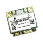
AzureWave IEEE 802.11ah Wireless LAN Module

Specifications
- Model: AW-HM593
- Standard: IEEE 802.11ah Wireless LAN
- Operating Frequency: 850 ~ 950MHz
- Data Rate: Up to 32.5Mbps
- Channel Width Options: 1/2/4/8 MHz
- Modulation: BPSK, QPSK, 16-QAM, 64-QAM
- Supported MCS Levels: MCS 0-7, MCS 10
- Security Features: WPA3, AES encryption engine, SHA1, SHA2 hash
functions - Interfaces: SDIO/SPI, I2C, UART
Product Usage Instructions
Installation and Setup
- Insert the AW-HM593 module into the appropriate slot on your device.
- Connect the necessary peripheral interfaces such as SDIO, SPI, I2C, and UART.
- Ensure proper antenna connection for optimal performance.
Configuration
Configure the module by following these steps
- Access the module’s configuration interface through the designated host interface.
- Set the desired channel width and modulation scheme based on your requirements.
- Configure security settings such as encryption type and key management.
Operation
To operate the AW-HM593 module
- Power on your device and ensure the module is powered up.
- Establish a connection to an existing Wi-Fi network or set up the module as an access point.
- Monitor data transfer rates and signal strength for optimal performance.
FAQ
Q: What is the operating range of the AW-HM593 module?
A: The AW-HM593 offers up to 1KM long-range data transfer capabilities.
Features
General
- Support programmable operation between 850 ~ 950MHz
- Support single-stream data rate up to 32.5Mbps (MCS=7, 64-QAM, 8MHz channel, 4 uSec GI)
- Support channel width options of 1/2/4/8 MHz
- Support Modulation and Coding Scheme (MCS) levels MCS 0-7 and MCS 10
- Modulation: BPSK & QPSK, 16-QAM & 64- QAM
- Support 1 MHz duplicate mode
Host interface
- SDIO 2.0 (slave) Default Speed (DS) at 25MHz
- SDIO 2.0 (slave) High Speed (HS) at 50MHz
- Support for both 1-bit and 4-bit data mode
- Support for SPI mode operation
Standards Supported
- IEEE Std 802.11ah-2016 compliant
Security Features
- AES encryption engine
- Hardware support for SHA1 and SHA2 hash functions (SHA-256, SHA-384,SHA-512)
- WPA3 including protected management frames (PMF)
- Opportunistic Wireless Encryption (OWE)
Peripheral Interfaces
- SDIO/SPI, I2C and UART
- Support for STA and AP roles
Revision History
Document NO: R2-2593-DST-01
| Version | Revision Date | DCN NO. | Description | Initials | Approved |
| A | 2022/06/29 | DCN026640 |
|
Daniel Lee | N.C. Chen |
| B | 2023/12/14 | DCN030777 |
|
Daniel Lee | N.C. Chen |
| C | 2024/05/21 | DCN031435 |
|
Daniel Lee | N.C. Chen |
| D | 2024/06/03 |
|
Daniel Lee | N.C. Chen | |
Introduction
Product Overview
AzureWave Technologies, Inc. introduces the pioneer of the IEEE 802.11ah WIFI stamp module — AW-HM593. The AW-HM593 is an IEEE 802.11ah Wi-Fi module that operates in the Sub 1GHz license-exempt band, offering longer ranger and higher data rate for internet of things (IoT) applications. The AW-HM593 enables streamlined data transfer interoperability with existing Wi-Fi networks while meeting up to 1KM long range data transfer with low power consumption requirements.
The AW-HM593 integrated Morse Micro MM6108 and external RF front end module (FEM) which can increase transmission power. MM6108 supports SDIO 2.0 compliant slave interface and SPI mode operation, and many peripherals such as general I2C, UART and GPIOs. In addition, its MAC supports for STA and AP roles.
Specifications Table
General
| Features | Description |
| Product Description | IEEE 802.11ah Wireless LAN Module |
| Major Chipset | Morse Micro MM6108 (48-pin QFN) |
| Host Interface | SDIO/SPI |
| Dimension | 14mm x 18.5mm x 2.25mm
(Tolerance remarked in mechanical drawing) |
| Form Factor | Stamp module, 38 pins |
| Antenna | l For Stamp Module, “1T1R, external” ANT Main:TX/RX
Model: AN0915-5001BSM, Type: Dipole Antenna, Gain: 2.34dBi |
| Weight | 1.0g |
1.2.2 WLAN
| Features | Description | ||||||
| WLAN Standard | IEEE 802.11ah | ||||||
| Frequency Rage | US (903.5 – 926.5 MHz) | ||||||
| Modulation | OFDM, BPSK, QPSK, 16-QAM, 64-QAM | ||||||
| Channel Bandwidth | 1/2/4/8 MHz | ||||||
| Output Power (Board Level Limit)* | Min | Typ | Max | Unit | |||
| MCS0 (1/2 MHz)
@EVM≦-5dB |
18 |
20 |
22 |
dBm |
|||
| MCS0 BW-4MHz 906MHz (Ch8)
@EVM≦-5dB |
18 |
20 |
22 |
dBm |
|||
| MCS0 BW-4MHz 914MHz (Ch24)
@EVM≦-5dB |
18 |
20 |
22 |
dBm |
|||
| MCS0 BW-4MHz 926MHz (Ch48)
@EVM≦-5dB |
15 |
17 |
19 |
dBm |
|||||
| MCS0 BW-8MHz 908MHz (Ch12)
@EVM≦-5dB |
18 |
20 |
22 |
dBm |
|||||
| MCS0 BW-8MHz 916MHz (Ch28)
@EVM≦-5dB |
18 |
20 |
22 |
dBm |
|||||
| MCS0 BW-8MHz 924MHz (Ch44)
@EVM≦-5dB |
17 |
19 |
21 |
dBm |
|||||
| MCS7 (1/2/4/8 MHz) @EVM≦-27dB |
14 |
16 |
18 |
dBm |
|||||
| Receiver Sensitivity | |||||||||
| Min | Typ | Max | Unit | ||||||
| MCS0 (1 MHz) | -104 | -100 | dBm | ||||||
| MCS0 (2 MHz) | -101 | -97 | dBm | ||||||
| MCS0 (4 MHz) | -99 | -95 | dBm | ||||||
| MCS0 (8 MHz) | -95 | -91 | dBm | ||||||
| MCS7 (1 MHz) | -87 | -81 | dBm | ||||||
| MCS7 (2 MHz) | -84 | -78 | dBm | ||||||
| MCS7 (4 MHz) | -81 | -75 | dBm | ||||||
| MCS7 (8 MHz) | -78 | -72 | dBm | ||||||
| Data Rate |
|
||||||||
| Security |
|
||||||||
Operating Conditions
| Features | Description |
| Operating Conditions | |
| Voltage | VBAT: 3.3V VDD_FEM: 3.3V VDDIO: 3.3V |
| Operating Temperature | -40℃~85 ℃ |
| Operating Humidity | less than 85%R.H |
| Storage Temperature | -40℃~90 ℃ |
| Storage Humidity | less than 60%R.H |
| ESD Protection | |
| Human Body Model | +/-1000V (RF Input pin.38), +/-2000V (All pins except RF Input) |
| Changed Device Model | +/-500V (All pins) |
Pin Definition
Pin Map

Pin Table
| Pin No. | Definition | Basic Description | Voltage | Type |
| 1 | GND | GROUND | GND | |
| 2 | GND | GROUND | GND | |
| 3 | GND | GROUND | GND | |
| 4 | MM_JTAG_TCK | JTAG clock | I | |
| 5 | MM_JTAG_TDI | JTAG data input | I | |
| 6 | NC | No Connection | ||
| 7 | MM_JTAG_TMS | JTAG mode selection | I | |
| 8 | MM_JTAG_TRST | JTAG reset | I | |
| 9 | MM_JTAG_TDO | JTAG data output | O | |
| 10 | NC | No Connection | I | |
| 11 | MM_GPIO10 | General purpose I/O | I/O | |
| 12 | GND | GROUND | GND | |
| 13 | MM_GPIO9 | General purpose I/O | I/O | |
| 14 | MM_GPIO8 | General purpose I/O | I/O | |
| 15 | MM_GPIO7 | General purpose I/O | I/O | |
| 16 | MM_SD_D1 | SDIO Data pin 1 | I/O | |
| 17 | MM_SD_D0 | SDIO Data pin 0 | I/O | |
| 18 | MM_SD_CLK | SDIO Clock pin (input) | I | |
| 19 | VDDIO | I/O supply Input | Power | |
| 20 | GND | GROUND | GND | |
| 21 | MM_SD_CMD | SDIO Command pin | I/O | |
| 22 | MM_SD_D3 | SDIO Data pin 3 | I/O | |
| 23 | MM_SD_D2 | SDIO Data pin 2 | I/O |
| 24 | MM_GPIO6 | General purpose I/O | I/O | |
| 25 | VBAT | 3.3V power supply | 3.3V | Power |
| 26 | GND | GROUND | GND | |
| 27 | MM_GPIO5 | General purpose I/O | I/O | |
| 28 | MM_GPIO4 | General purpose I/O | I/O | |
| 29 | MM_GPIO3 | General purpose I/O | I/O | |
| 30 | MM_GPIO2 | General purpose I/O | I/O | |
| 31 | GND | GROUND | GND | |
| 32 | VDD_FEM | Front End Module power input | 3.3V | Power |
| 33 | MM_GPIO1 | General purpose I/O | I/O | |
| 34 | Busy | WiFi Busy | I/O | |
| 35 | MM_RESET_N | Reset (active low) | I/O | |
| 36 | MM_WAKE | WAKE from sleep | I | |
| 37 | GND | GROUND | GND | |
| 38 | ANT | RF IN/OUT | I/O |
Electrical Characteristics
Absolute Maximum Ratings
| Symbol | Parameter | Minimum | Typical | Maximum | Unit |
| VDD_FEM | Front End Module power input | -0.5 | – | 5.5 | V |
| VBAT | 3.3V power supply | -0.5 | – | 4.3 | V |
| VDDIO | I/O supply Input | -0.5 | – | 4.3 | V |
| Tstg | Storage temperature | -40 | – | 90 | ℃ |
Recommended Operating Conditions
| Symbol | Parameter | Minimum | Typical | Maximum | Unit |
| VDD_FEM | Front End Module power input | 3.0 | 3.3 | 3.6 | V |
| VBAT | 3.3V power supply | 3.0 | 3.3 | 3.6 | V |
| VDDIO | 3.3V I/O supply Input | 1.8 | 3.3 | VBAT | V |
| TAMBIENT | Ambient temperature | -40 | 25 | 85 | ℃ |
Timing Sequence
SDIO Bus Timing
The SDIO clock rate supports up to 50MHz. The device always operates in SD high speed mode.

 SPI Bus
The SPI clock rate supports up to 50MHz. The SPI bus timing is identical to the SDIO bus timing, where MOSI and MISO are considered input and output timing, respectively, in the SDIO timing specification.
The SPI bus defaults to clock idling at logical 0 (CPOL=0), and data is launched and captured on the positive edges of the clock, as per SDIO high-speed mode. It may be configured to behave like CPHA=0 (drive output on negative edge, sample on positive edge) after being initialized.
UART Bus
Two universal asynchronous receiver/transmitter (UARTs) are available and provide a means for serial communication to off-chip devices. The UART cores are as-provided by the SiFive IP repository. The UART peripheral does not support hardware flow control or other modem control signals, or synchronous serial data transfers.
We will clock the UARTs with a maximum clock speed of 30MHz (TBD), meaning maximum baud of the UART will be around 30Mbaud or 30Mbits/s if a divisor of 0 is specified.
| Pin | Name | Default Function | I/O Function |
| 15 | MM_GPIO7 | GPIO | UART1 Tx |
| 24 | MM_GPIO6 | GPIO | UART1 Rx |
| 29 | MM_GPIO3 | GPIO | UART0 Tx |
| 30 | MM_GPIO2 | GPIO | UART0 Rx |
I2C Bus Timing
An I2C master interface is available. It consists of two lines, SDA and SCL, which are bidirectional, connected to a positive supply voltage via a current-source or pull-up resistor.
| Pin | Name | Default Function | I/O Function |
| 27 | MM_GPIO5 | GPIO | I2C SCL |
| 28 | MM_GPIO4 | GPIO | I2C SDA |
Definition of timing for F/S-mode devices on the I2C-bus. All values referred to 
 Power Consumption
Transmit Power Consumption
| Band (MHz) |
Modulation |
BW (MHz) |
DUT Condition |
VBAT = 3.3V, VDD_FEM = 3.3V | |
| VBAT (mA) | VDD_FEM (mA) | ||||
| Avg. | Avg. | ||||
|
915 |
MCS0 |
1 |
Tx @ 20 dBm |
68.5 | 140.4 |
| 2 | 68.3 | 124.3 | |||
| 4 | 71.7 | 108.2 | |||
| 8 | 78.7 | 92.2 | |||
|
MCS7 |
1 |
Tx @ 16 dBm |
59.8 | 80.2 | |
| 2 | 57.7 | 60.1 | |||
| 4 | 61.8 | 52.7 | |||
| 8 | 69.6 | 49.2 | |||
* The power consumption is based on AzureWave test environment, these data for reference only.
Receive Power Consumption
| Band (MHz) | Modulation | BW (MHz) | DUT Condition | VBAT = 3.3V, VDD_FEM = 3.3V | ||
| VBAT (mA) | VDD_FEM (mA) | |||||
| Avg. | Avg. | |||||
|
915 |
MCS0 |
1 | Continuous Rx @ -95 dBm | 40.4 | 4.8 | |
| 2 | Continuous Rx @ -92 dBm | 43.2 | 4.8 | |||
| 4 | Continuous Rx @ -89 dBm | 50.2 | 4.8 | |||
| 8 | Continuous Rx @ -86 dBm | 66.5 | 4.8 | |||
|
MCS7 |
1 | Continuous Rx @ -77 dBm | 41.0 | 4.8 | ||
| 2 | Continuous Rx @ -74 dBm | 43.7 | 4.8 | |||
| 4 | Continuous Rx @ -71 dBm | 49.9 | 4.8 | |||
| 8 | Continuous Rx @ -68 dBm | 62.5 | 4.8 | |||
* The power consumption is based on AzureWave test environment, these data for reference only.
Mechanical Information
Mechanical Drawing

Packing Information
- One reel can pack 1000pcs
- One production label is pasted on the reel, one desiccant and one humidity indicator card are put on the reel
- One reel is put into the anti-static moisture barrier bag, and then one label is pasted on the bag
- A bag is put into the anti-static pink bubble wrap

- A bubble wrap is put into the inner box and then one label is pasted on the inner box
- 4 inner boxes could be put into one carton
- Sealing the carton by AzureWave tape

- One carton label and one box label are pasted on the carton. If one carton is not full, one balance label pasted on the carton


Warning Statements
Federal Communication Commission Interference Statement
This equipment has been tested and found to comply with the limits for a Class B digital device, pursuant to Part 15 of the FCC Rules. These limits are designed to provide reasonable protection against harmful interference in a residential installation. This equipment generates, uses and can radiate radio frequency energy and, if not installed and used in accordance with the instructions, may cause harmful interference to radio communications. However, there is no guarantee that interference will not occur in a particular installation. If this equipment does cause harmful interference to radio or television reception, which can be determined by turning the equipment off and on, the use is encouraged to try to correct the interference by one of the following measures:
- Reorient or relocate the receiving antenna.
- Increase the separation between the equipment and receiver.
- Connect the equipment into an outlet on a circuit different from that to which the receiver is connected.
- Consult the dealer or an experienced radio/TV technician for help.
FCC Caution
Any changes or modifications not expressly approved by the party responsible for compliance could void the user’s authority to operate this equipment.
This device complies with Part 15 of the FCC Rules. Operation is subject to the following two conditions:
- This device may not cause harmful interference, and
- this device must accept any interference received, including interference that may cause undesired operation.
FCC Radiation Exposure Statement:
This equipment complies with FCC radiation exposure limits set forth for an uncontrolled environment. This equipment should be installed and operated with a minimum distance 20cm between the radiator and your body.
IMPORTANT NOTE:
This module has been tested and found to comply with the following requirements for Modular Approval.
Part 15.247 – Operation within the bands 902-928 MHz, 2400-2483.5 MHz, and 5725-5850 MHz.
RF exposure considerations
In the end product, the antenna(s) used with this transmitter must be installed to provide a separation distance of at least 20cm from all persons and must not be co-located or operation in conjunction with any other antenna or transmitter except in accordance with multi-transmitter product procedures. User and installers must be provided with antenna installation instructions and transmitter operating conditions for satisfying the RF exposure compliance.
Antennas
This radio transmitter has been approved by the FCC to operate with the antenna types listed below with the maximum permissible gain indicated. Antenna types not included in this list, having a gain greater than the maximum gain indicated for that type, are strictly prohibited for use with this device.
| Radio | Antenna Type | Freq. (MHz) | Peak Antenna Gain (dBi) |
| 802.11 ah | Dipole | 902 – 928 | 2.34 |
Required End Product Labeling
Any device incorporating this module must include an external, visible, permanent marking or label which states: “Contains FCC ID: TLZ-HM593”
Test Modes
This device uses various test mode programs for test set up which operate separate from production firmware. Host integrators should contact the grantee for assistance with test modes needed for module/host compliance test requirements.
Additional testing, Part 15 Subpart B disclaimer
The modular transmitter is only FCC authorized for the specific rule parts (i.e. FCC
transmitter rules) listed on the grant, and that the host product manufacturer is responsible for compliance to any other FCC rules that apply to the host not covered by the modular transmitter grant of certification.
The final host product still requires Part 15 Subpart B compliance testing with the modular transmitter installed.
EMI Considerations
Note that a host manufacture is recommended to use KDB996369 D04 Module Integration Guide recommending as “best practice” RF design engineering testing and evaluation in
case non-linear interactions generate additional non-compliant limits due to module placement to host components or properties.
For standalone mode, reference the guidance in KDB996369 D04 Module Integration Guide and for simultaneous mode; see KDB996369 D02 Module Q&A Question 12, which permits the host manufacturer to confirm compliance.
How to make changes
Only Grantees are permitted to make permissive changes, if the module will be used differently than granted conditions, please contact us to ensure modifications will not affect compliance.
Antenna Trace Design
The modular transmitter is configured for monostatic operation, which requires only a single RF I/O pin for full duplex communication. The output must be routed to the antenna via 50 ohm microstrip or strapline on the OEM PCB. No coupling capacitor is required given that the RF pin is AC-coupled internally.

- Length: 40.9mm
- Width: 0.28mm
- Thickness: 0.18mm
- Type of trace: 1oz
- Dielectric constant: 4.2
- Antenna connector: 50ohm SMA Male
- The trace from Pin No. 38 to antenna connector on the OEM PCB must be maintained identical as the above specification with Reversed SMA connector. Only trace designs approved with an original grant or through permissive change can be used by an OEM, any changes are deemed as antenna type change and should be reviewed to ensure compliance with the FCC and ISED requirements.
- Verification must be conducted and the results shall not exceed below ranges to ensure identical antenna design is applied to subsequent integration and end product production.
- Impedance 50 ohm +/- 10%
- Input power is 21.5dBm (Average power)
- VSWR absolute max 5dBm (Average power) subsequent integrat
- VSWR recommended 5dBm (Average power) subsequent integration and end pr
Test procedure of verification
- Set module device in support transmission mode.
- Verify RF power through conducted measurement at balanced impedance of 50ohms, the KDB 971168 D01 Power Meas License Digital System shall be used as the supplemental test methodology to adjust the proper setting obtaining the measurement results.
- Verify the Tx power in the datasheet, and compliance test reports.
Innovation, Science and Economic Development Statement
This device contains license-exempt transmitter(s) / receiver(s) that comply with Innovation, Science and Economic Development Canada’s license-exempt RSS(s). Operation is subject to the following two conditions:
- This device may not cause interference, and
- This device must accept any interference, including interference that may cause undesired operation of the device.
Antennas
This radio transmitter has been approved by the ISED to operate with the antenna types listed below with the maximum permissible gain indicated. Antenna types not included in this list, having a gain greater than the maximum gain indicated for that type, are strictly prohibited for use with this device.
| Radio | Antenna Type | Freq. (MHz) | Peak Antenna Gain (dBi) |
| 802.11 ah | Dipole | 902 – 928 | 2.34 |
Required End Product Labeling
Any device incorporating this module must include an external, visible, permanent marking or label which states: “Contains IC: 6100A-HM593”
FORM NO.: FR2-015_ A Responsible Department:WBU Expiry Date: Forever The information contained herein is the exclusive property of AzureWave and shall not be distributed, reproduced, or disclosed in whole or in part without prior written permission of AzureWave.
Documents / Resources
 |
AzureWave IEEE 802.11ah Wireless LAN Module [pdf] User Guide IEEE 802.11ah Wireless LAN Module, IEEE 802.11ah, Wireless LAN Module, LAN Module, Module |