AzureWave AW-CM358MA Wireless MCU with Integrated Wi-Fi 6 Microcontroller Module
Product Usage Instructions
Installation
Ensure the AW-CU603 module is properly aligned with the corresponding connectors on your device.
Power Supply
Connect a single 3.3 V power supply to the AW-CU603 module.
Connectivity
Utilize the UART, I2C, or USB interface for establishing connectivity with the AW-CU603 module.
Network Setup
Configure the Wi-Fi settings on your device to connect to the AW-CU603 module.
Features
WLAN
- 1×1 dual-band 2.4 GHz/5 GHz Wi-Fi 6 radio
- 20 MHz channel operation
- Wi-Fi 6 Target Wake Time(TWT) support
- Wi-Fi 6 Extended Range (ER) and Dual Carrier Modulation (DCM)
- Low-power Wi-Fi idle, standby, and sleep modes
- WPA/WPA2/WPA3 personal and enterprise
- Support for Matter over Wi-Fi
Revision History
Document NO: R2-2603-DST-01
| Version | Revision Date | DCN NO. | Description | Initials | Approved |
| A | 2024/05/07 | DCN031572 | l Draft version | Roger Liu | N.C Chen |
Introduction
Product Overview
AzureWave AW-CU603 is a highly integrated, low-power Wireless RW610 MCU with an integrated MCU and Wi-Fi 6 designed for a broad array of applications. Applications include connected smart home devices, enterprise and industrial automation, smart accessories, and smart energy. AW-CU603 includes a 260 MHz Arm Cortex-M33 core with Trust Zone-M, 1.2 MB on-chip SRAM and a Quad SPI interface with high bandwidth, and an on-the-fly decryption engine for securely accessing off-chip XIP flash. AW-CU603 includes a full-featured 1×1 dual-band (2.4 GHz / 5 GHz) 20 MHz Wi-Fi 6 (802.11ax) subsystem bringing higher throughput, better network efficiency, lower latency, and improved range over previous generation Wi-Fi standards. The advanced design of the AW-CU603 delivers tight integration, low power, and highly secure operation in a space- and cost-efficient wireless MCU requiring only a single 3.3 V power supply.
Block Diagram
TBD
Specifications Table
General
| Features | Description |
| Product Description | Wi-Fi 6 1×1 Microcontroller Module |
| Major Chipset | NXP RW610 HVQFN (116 pins) |
| Host Interface | UART / I2C / USB |
| Dimension | 22 mm x 30 mm x 2.45 mm |
| Package | M.2 2230 |
| Antenna | I-PEX MHF4 Connector Receptacle (20449) 1×1 diversity on MAIN ANT and AUX ANT |
| Weight | 2.64g |
WLAN
| Features | Description |
| WLAN Standard | IEEE 802.11 a/b/g/n/ac/ax 1T1R |
| WLAN VID/PID | NA |
| WLAN SVID/SPID | NA |
| Frequency Rage |
|
| Modulation | DSSS, OFDM, DBPSK, DQPSK, CCK,16-QAM, 64-QAM, 256-QAM, |
| Number of Channels | 2.4GHz:
5GHz:
|
149, 153, 157, 161, 165, 169, 173, 177
|
|||||||||||||||||||||||||||||||||||||||||||||||||||||||||
| Output Power (Board Level Limit)* | 2.4G
5G |
||||||||||||||||||||||||||||||||||||||||||||||||||||||||
| Min | Typ | Max | Unit | ||||||||||||||||||||||||||||||||||||||||||||||||||||||
| 11a (54Mbps) @EVM≦-25 dB | 14 | 16 | 18 | dBm | |||||||||||||||||||||||||||||||||||||||||||||||||||||
| 11n (HT20 MCS7) @EVM≦-27 dB | 13 | 15 | 17 | dBm | |||||||||||||||||||||||||||||||||||||||||||||||||||||
| 11ac(VHT20 MCS8) @EVM≦-30 dB | 12 | 14 | 16 | dBm | |||||||||||||||||||||||||||||||||||||||||||||||||||||
| 11ax(HE20 MCS9) @EVM≦-32 dB | 11 | 13 | 15 | dBm | |||||||||||||||||||||||||||||||||||||||||||||||||||||
| Receiver Sensitivity | 2.4G
5G
|
||||||||||||||||||||||||||||||||||||||||||||||||||||||||
| Data Rate | WLAN: 802.11b : 1, 2, 5.5, 11Mbps 802.11a/g : 6, 9, 12, 18, 24, 36, 48, 54Mbps 802.11n : Maximum data rates up to 72 Mbps (20 MHz channel) 802.11ac: Maximum data rates up to 87 Mbps (20 MHz channel) 802.11ax: Maximum data rates up to 115 Mbps (20 MHz channel) |
| Security | n Wi-Fi: WPA2/WPA3 personal and enterprise and AES/CCMP/CMAC/GCMP |
- * If you have any certification questions about output power please contact FAE directly.
Operating Conditions
| Features | Description |
| Operating Conditions | |
| Voltage | 3.3V +-5% |
| Operating Temperature | -40℃ to +85℃ |
| Operating Humidity | Less than 85% R.H. |
| Storage Temperature | -40℃ to +85℃ |
| Storage Humidity | Less than 60% R.H. |
| ESD Protection | |
| Human Body Model | TBD |
| Changed Device Model | TBD |
Pin Definition
Pin Map
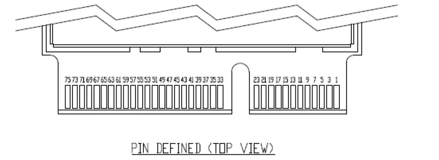
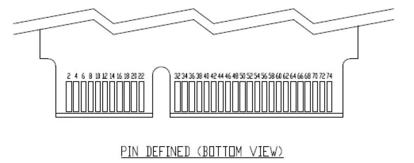
Pin Table
| Pin No | Definition | Basic Description | Voltage | Type |
| 1 | GND | Ground | GND | |
| 2 | +3.3V | 3.3V power supply. | 3.3V | Power |
| 3 | USB_D+ | USB bus data+ | 3.3V | I/O |
| 4 | +3.3V | 3.3V power supply | 3.3V | Power |
| 5 | USB_D- | USB bus data- | 3.3V | I/O |
| 6 | LED1# | GPIO[11], PWM output | 3.3V | I/O |
| 7 | GND | Ground | GND | |
| 8 | NC | No connect to anything | Floating | |
| 9 | NC | No connect to anything | Floating | |
| 10 | NC | No connect to anything | Floating | |
| 11 | NC | No connect to anything | Floating | |
| 12 | NC | No connect to anything | Floating | |
| 13 | NC | No connect to anything | Floating | |
| 14 | NC | No connect to anything | Floating | |
| 15 | NC | No connect to anything | Floating | |
| 16 | LED2# | GPIO[42], ADC0 channel 0 | 3.3V | I/O |
| 17 | NC | No connect to anything | Floating | |
| 18 | GND | Ground. | GND | |
| 19 | GND | Ground. | GND | |
| 20 | UART WAKE# | UART Host Wake | 3.3V | O |
| 21 | NC | No connect to anything | Floating | |
| 22 | UART TxD | UART_SOUT | 3.3V | O |
| 23 | NC | No connect to anything | Floating | |
| 32 | UART RxD | UART_SIN | 3.3V | I |
| 33 | GND | Ground. | GND | |
| 34 | UART RTS | UART_RTS | 3.3V | O |
| 35 | NC | No connect to anything | Floating | |
| 36 | UART CTS | UART_CTS | 3.3V | I |
| 37 | NC | No connect to anything | Floating | |
| 38 | Board ID | GPIO[43] | 3.3V | I/O |
| 39 | GND | Ground | GND | |
| 40 | CONFIG_HOST_BOOT[0] | Host configuration options HW Strap pin for ISP boot mode or for programing Flash | 1.8V | I/O |
| 1= Boot from Flex SPI Flash (Default) 0= ISP boot from UART to programing flash |
||||
| 41 | NC | No connect to anything | Floating | |
| 42 | Vendor defined | Reserve No connect to anything | Floating | |
| 43 | NC | No connect to anything | Floating | |
| 44 | Alert# _EC | GPIO[22] | 3.3V | O |
| 45 | GND | Ground | GND | |
| 46 | I2C1_DATA | GPIO[9] FC1_RXD_SDA_MOSI_DATA_I2C:Flexcomm1 I2C data in/out | 3.3V | I/O |
| 47 | NC | No connect to anything | Floating | |
| 48 | I2C1_CLK | GPIO[8] FC1_TXD_SCL_MISO_WS_I2C:Flexcomm1 I2C clock | 3.3V | I/O |
| 49 | NC | No connect to anything | Floating | |
| 50 | NC | No connect to anything | Floating | |
| 51 | GND | Ground | GND | |
| 52 | NC | No connect to anything | Floating | |
| 53 | NC | No connect to anything | Floating | |
| 54 | NC | No connect to anything | Floating | |
| 55 | NC | No connect to anything | Floating | |
| 56 | W_DISABLE1# | Full Power-down (input) (active low)0 = full power-down mode1 = normal mode This pin has internal pull high 51k resistor to 3.3V | 3.3V | I |
| 57 | GND | Ground | GND | |
| 58 | I2C0_DATA | GPIO[2] FC0_RXD_SDA_MOSI_DATA_I2C:Flexcomm0 I2C data in/out | 3.3V | I/O |
| 59 | NC | No connect to anything | Floating | |
| 60 | I2C0_CLK | GPIO[3] FC0_TXD_SCL_MISO_WS_I2C:Flexcomm0 I2C clock | 3.3V | I/O |
| 61 | NC | No connect to anything | Floating | |
| 62 | ALERT# | GPIO[27] | 3.3V | O |
| 63 | GND | Ground | GND | |
| 64 | NC | No connect to anything | Floating | |
| 65 | NC | No connect to anything | Floating | |
| 66 | NC | No connect to anything | Floating |
| 67 | NC | No connect to anything | Floating | |
| 68 | NC | No connect to anything | Floating | |
| 69 | GND | Ground | GND | |
| 70 | NC | No connect to anything | Floating | |
| 71 | NC | No connect to anything | Floating | |
| 72 | +3.3V | 3.3V power supply | 3.3V | Power |
| 73 | NC | No connect to anything | Floating | |
| 74 | +3.3V | 3.3V power supply | 3.3V | Power |
| 75 | GND | Ground | GND |
Electrical Characteristics
Absolute Maximum Ratings
| Symbol | Parameter | Minimum | Typical | Maximum | Unit |
| VBAT | DC supply for the 3.3V input | – | 3.3 | 3.96 | V |
| VIO | 1.8 V/3.3 V digital I/O power supply | – | 1.8 | 2.16 | V |
| 3.3 | 3.96 | V |
Recommended Operating Conditions
| Symbol | Parameter | Minimum | Typical | Maximum | Unit |
| VBAT | DC supply for the 3.3V input | 3.14 | 3.3 | 3.46 | V |
| VIO | 1.8 V/3.3 V digital I/O power supply | 1.71 | 1.8 | 1.89 | V |
| 3.14 | 3.3 | 3.46 | V |
Digital IO Pin DC Characteristics
VIO 1.8V Operation
| Symbol | Parameter | Minimum | Typical | Maximum | Unit |
| VIO | I/O pad supply voltage | 1.62 | 1.8 | 1.98 | V |
| VIH | Input high voltage | 0.7*VIO | – | VIO+0.4 | V |
| VIL | Input low voltage | -0.4 | – | 0.3*VIO | |
| VOH | Output High Voltage | VIO-0.4 | – | – | |
| VOL | Output Low Voltage | – | – | 0.4 | |
| VHYS | Input Hysteresis | 100 | mV |
VIO 3.3V Operation
| Symbol | Parameter | Minimum | Typical | Maximum | Unit |
| VIO | I/O pad supply voltage | 2.97 | 3.3 | 3.63 | V |
| VIH | Input high voltage | 0.7*VIO | – | VIO+0.4 | V |
| VIL | Input low voltage | -0.4 | – | 0.3*VIO |
| VOH | Output High Voltage | VIO-0.4 | – | – | |
| VOL | Output Low Voltage | – | – | 0.4 | |
| VHYS | Input Hysteresis | 100 | mV |
Power On Sequence
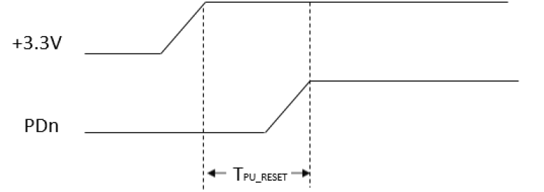
| Symbol | Parameter | Min | Typ | Max | Units |
| Tpu_reset | Valid power to PDn deasserted | 0 | – | – | ms |
Power Consumption
WLAN
| Band (GHz) | Mode | BW(MHz) | RF Power (dBm) | VBAT_IN=3.3 V | |
| Transmit | |||||
| Max. | Avg. | ||||
| 2.4 | 11b@1Mbps | 20 | 18 | 291 | 286 |
| 11g@54Mbps | 20 | 16 | 266 | 251 | |
| 11n@MCS7 | 20 | 15 | 243 | 230 | |
| 11ax@MCS0 NSS1 | 20 | 14 | 235 | 230 | |
| 11ax@MCS11 NSS1 | 20 | 14 | 240 | 222 | |
| 5 | 11a@6Mbps | 20 | 16 | 391 | 384 |
| 11n@MCS7 | 20 | 15 | 375 | 354 | |
| 11ac@MCS0 NSS1 | 20 | 14 | 352 | 347 | |
| 11ac@MCS8 NSS1 | 20 | 14 | 350 | 327 | |
| 11ax@MCS0 NSS1 | 20 | 13 | 340 | 334 | |
| 11ax@MCS11 NSS1 | 20 | 13 | 337 | 315 | |
| Band (GHz) | Mode | BW(MHz) | Receive | ||
| Max. | Avg. | ||||
| 2.4 | 11b@11Mbps | 20 | 90 | 86 | |
| 11g@54Mbps | 20 | 92 | 89 | ||
| 11n@MCS7 | 20 | 91 | 88 | ||
| 11ax@MCS11 NSS1 | 20 | 87 | 83 | ||
| 5 | 11a@54Mbps | 20 | 108 | 104 | |
| 11n@MCS7 | 20 | 109 | 104 | ||
| 11ac@MCS8 NSS1 | 20 | 107 | 104 | ||
| 11ax@MCS11 NSS1 | 20 | 107 | 102 | ||
Current Unit: mA
Normal Mode
| VBAT_IN=3.3V | ||||||||
| MCU Status | WiFi Deep Sleep | WiFi STA Connected | WiFi IEEE Power Saving | WiFi Power Down | ||||
| 2.4G | 5G | 2.4G | 5G | |||||
| DTIM 1 | DTIM10 | DTIM1 | DTIM10 | |||||
| PM0(Active) | 27.1 | 71.8 | 91.5 | NA | 27.2 | |||
| PM1(Idle) | 18.3 | 62.8 | 83.5 | 21.1 | 18.8 | 19.4 | 18.6 | 18.4 |
| PM2(Standby) | 7.1 | 51.9 | 72.5 | 10.2 | 7.7 | 8.2 | 7.6 | 7.0 |
| PM3(Sleep) | 2.7 | 50.3 | 71.2 | 6.0 | 3.2 | 3.8 | 3.7 | 2.7 |
| PM4(Shutdown) | NA | NA | NA | NA | ||||
Current Unit: mA
Peak Current
| No. | Item | VBAT=3.3 V |
| Max. | ||
| 1 | Peak current during device initialization | 547 |
| 2 | Peak current during device scan AP | 534 |
| 3 | Peak current during device connect AP | 515 |
Current Unit: mA
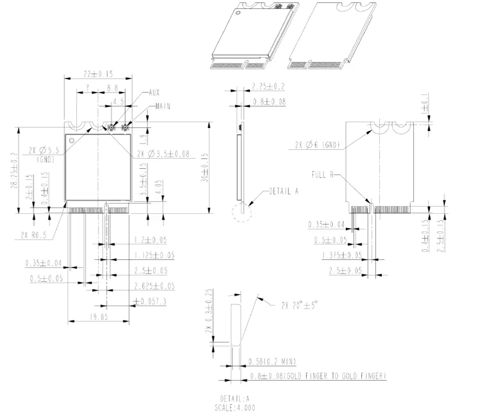
Mechanical Information
Mechanical Drawing
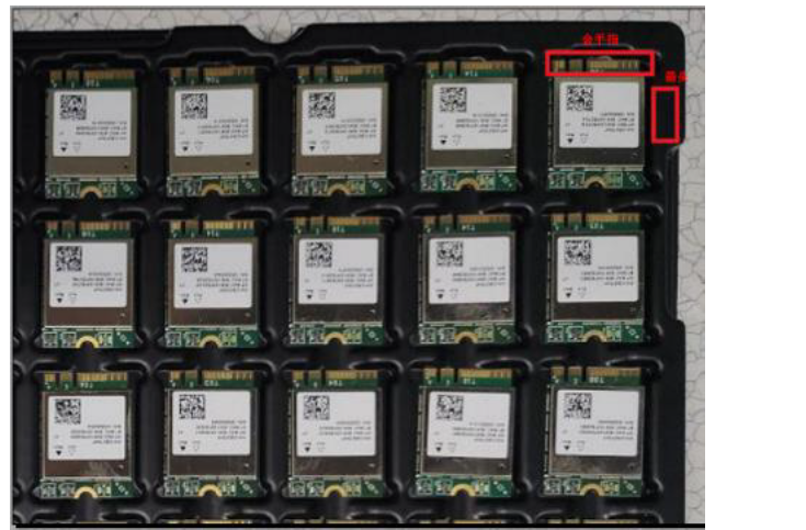
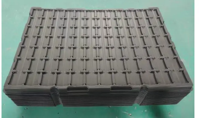
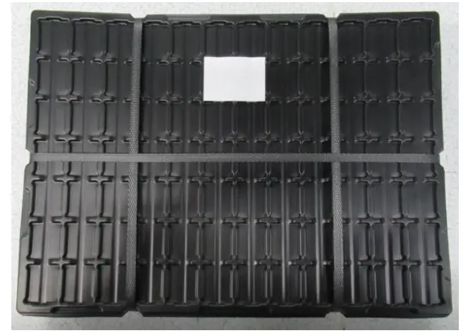
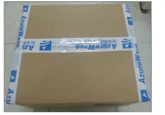
Packing Information
- 84pcs M.2 2230 modules put in one tray
- The trays are stacked with each other, and add more one tray on the top, so the total number of trays is 14pcs, i.e. 13pcs tray (full) and 1pcs tray (empty)
- Use P.P Strap to pack 14pcs trays and add one packing label on the top

- Put the two packed tray into the box
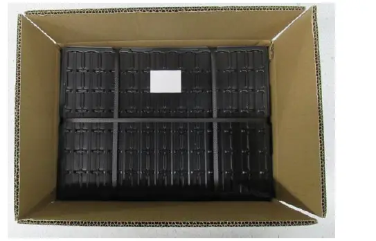
- Seal the carton by Azure Wave tape
- One carton label and one box label pasted on the carton. If the carton is not full, add one balance label pasted on the carton

Label Information on the carton
| Example of Packing Label |  |
|||
| Example of carton label |  |
|||
| Azure Wave P/N | AW-CU603 | |||
| Customer | Provided by Sales | |||
| Customer P/N | Provided by Sales | |||
| Customer P/O | Provided by Sales | |||
| Description | AW-CU603 | |||
| Q’ty | ||||
| C/N | ||||
| N.W. | G.W. | |||
| Example of box label |  |
|||
| Example of balance label |  |
|||
Note:
- 1 Packed Tray = 13pcs Tray = 1092 pcs
- 1 Carton = 2 Packed Tray = 2184 pcs
Federal Communication Commission Interference Statement
This device complies with Part 15 of the FCC Rules.
Operation is subject to the following two conditions:
- This device may not cause harmful interference, and
- This device must accept any interference received, including interference that may cause undesired operation.
This equipment has been tested and found to comply with the limits for a Class B digital device, pursuant to part 15 of the FCC Rules. These limits are designed to provide reasonable protection against harmful interference in a residential installation. This equipment generates, uses and can radiate radio frequency energy and, if not installed and used in accordance with the instructions, may cause harmful interference to radio communications. However, there is no guarantee that interference will not occur in a particular installation. If this equipment does cause harmful interference to radio or television reception, which can be determined by turning the equipment off and on, the user is encouraged to try to correct the interference by one or more of the following measures:
- Reorient or relocate the receiving antenna.
- Increase the separation between the equipment and receiver.
- Connect the equipment into an outlet on a circuit different from that to which the receiver is connected.
- Consult the dealer or an experienced radio/TV technician for help.
Changes or modifications not expressly approved by the party responsible for compliance could void the user‘s authority to operate the equipment.
Radiation Exposure Statement:
This equipment complies with FCC radiation exposure limits set forth for an uncontrolled environment. This equipment should be installed and operated with minimum distance 20cm between the radiator & your body.
Industry Canada Statement
CAN ICES-3(B)/ NMB-3(B)
This device contains licence-exempt transmitter(s)/receiver(s) that comply with Innovation, Science and Economic Development Canada’s licence-exempt RSS(s).
Radiation Exposure Statement:
This equipment complies with ISED radiation exposure limits set forth for an uncontrolled environment. This equipment should be installed and operated with greater than 20cm between the radiator & your body.
Caution :
- The device for operation in the band 5150-5250 MHz is only for indoor use to reduce the potential for harmful interference to co-channel mobile satellite systems;
- For devices with detachable antenna(s), the maximum antenna gain permitted for devices in the bands 5250-5350 MHz and 5470-5725 MHz shall be such that the equipment still complies with the e.i.r.p. limit;
- For devices with detachable antenna(s), the maximum antenna gain permitted for devices in the band 5725-5850 MHz shall be such that the equipment still complies with the e.i.r.p. limits as appropriate;
- Where applicable, antenna type(s), antenna models(s), and worst-case tilt angle(s) necessary to remain compliant with the e.i.r.p. elevation mask requirement set forth in section 6.2.2.3 shall be clearly indicated.
This module is limited to OEM installation ONLY.
List of applicable FCC rules
Compliance with FCC Part 15C, 15E regulation.
Specific operational use conditions
The module is tested for standalone mobile RF exposure use condition. Any other usage conditions such as co-location with other transmitter(s) will need a separate reassessment through a class II permissive change application or new certification.
Limited module procedures
Not applicable to this device
RF exposure considerations
This module is limited to installation in mobile or fixed applications, according to §2.1091(b). The separate approval is required for all other operating configurations, including portable configurations with respect to Part §2.1093 and different antenna configurations
Antennas:
- The antenna must be installed such that 20 cm is maintained between the antenna and users,
- The transmitter module may not be co-located with any other transmitter or antenna.
- To comply with FCC/IC regulations limiting both maximum RF output power and human exposure to RF radiation, the maximum antenna gain including cable loss in a mobile exposure condition must not exceed:
- Antenna Type: PIFA
- Antenna gain: 3.5 dBi in 2.4GHz (frequency); 5 dBi in 5 GHz (frequency)
- Antenna Connector (if applicable): IPEX MHF4
In the event that these conditions cannot be met (for example certain laptop configurations or co-location with another transmitter), then the FCC/IC authorization is no longer considered valid and the FCC ID/IC ID cannot be used on the final product. In these circumstances, the OEM integrator will be responsible for re-evaluating the end product (including the transmitter) and obtaining a separate FCC/IC authorization.
Label and compliance information
When the module is installed in the host device, the FCC ID/ IC ID label must be visible through a window on the final device or it must be visible when an access panel, door or cover is easily removed. If not, a second label must be placed on the outside of the final device that contains the following text: “Contains FCC ID: TLZ-CU603”, “Contains IC: 6100A-CU603 “
The grantee’s FCC ID/IC ID can be used only when all FCC/IC compliance requirements are met. The OEM integrator has to be aware not to provide information to the end user regarding how to install or remove this RF module in the user’s manual of the end product which integrates this module. The end user manual shall include all required regulatory information/warning as show in this manual.
Information on test modes and additional testing requirements
This radio module must not be installed to co-locate and operating simultaneously with other radios in the host system except in accordance with FCC multi-transmitter product procedures. Additional testing and equipment authorization may be required operate simultaneously with other radio.
Additional testing, Part 15 Subpart B disclaimer
The host manufacturer is required to show compliance with Part 15 Subpart B while the transmitter module(s) are installed and operating. The modules should be transmitting and the evaluation should confirm that the module’s intentional emissions are compliant (i.e. fundamental and out of band emissions). The host manufacturer must verify that there are no additional unintentional emissions other than what is permitted in Part 15 Subpart B or emissions are complaint with the transmitter(s) rule(s).
Note EMI Considerations
Please follow the guidance provided for host manufacturers in KDB publications 996369 D02 and D04.
How to make changes
Only Grantees are permitted to make permissive changes.
Please contact us if the host integrator expect the module to be used differently than as granted:
- Company Name: Azure Wave Technologies (USA), Inc.
- Company Address:467 Saratoga ave #108 San Jose, CA 95129 United States
- Japan : 5GHz band (W52,W53): Indoor use only (except communicate to W52 high power radio)
Frequently Asked Questions (FAQ)
- Q: What are the supported Wi-Fi standards?
A: The AW-CU603 supports Wi-Fi 6 (802.11ax) standards for enhanced performance. - Q: How do I ensure secure operation?
A: The module features Trust Zone-M and on-the-fly decryption engine for secure operation. Ensure proper encryption protocols are utilized. - Q: Can the AW-CU603 be used in smart home devices?
A: Yes, the AW-CU603 is suitable for connected smart home devices along with other applications like enterprise automation and smart accessories.
Documents / Resources
 |
AzureWave AW-CM358MA Wireless MCU with Integrated Wi-Fi 6 Microcontroller Module [pdf] User Manual CU603, TLZ-CU603, AW-CU603, AW-CM358MA Wireless MCU with Integrated Wi-Fi 6 Microcontroller Module, AW-CM358MA, Wireless MCU with Integrated Wi-Fi 6 Microcontroller Module, Integrated Wi-Fi 6 Microcontroller Module, Wi-Fi 6 Microcontroller Module, 6 Microcontroller Module, Microcontroller Module |