aspar RS485 8 Analogue Universal Inputs Module

Thank you for choosing our product.
This manual will help you with proper support and proper operation of the device.
The information contained in this manual have been prepared with utmost care by our professionals and serve as a description of the product without incurring any liability for the purposes of commercial law.
This information does not release you from the obligation of own judgment and verification.
We reserve the right to change product specifications without notice.
Please read the instructions carefully and follow the recommendations contained therein.
WARNING!
Failure to follow instructions can result in equipment damage or impede the use of the hardware or software.
Safety rules
- Before first use, refer to this manual
- Before first use, make sure that all cables are connected properly
- Please ensure proper working conditions, according to the device specifications (eg: supply voltage, temperature, maximum power consumption)
- Before making any modifications to wiring connections, turn off the power supply
Module Features
Purpose and description of the module
The MOD-8I8RO module is an innovative device that provides a simple and cost-effective extension of the number of lines of input and output in popular PLCs.
The module has 8 digital inputs with configurable timer/counter option and 8 digital outputs. In addition, terminals IN1 and IN2 and IN3 and IN4 can be used to connect two encoders. All inputs and outputs are isolated from the logic of using optocouplers. Each channel can be individually configured in one of several modes.
This module is connected to the RS485 bus with twisted-pair wire. Communication is via MODBUS RTU or MODBUS ASCII. The use of 32-bit ARM core processor provides fast processing and quick communication. The baud rate is configurable from 2400 to 115200.
The module is designed for mounting on a DIN rail in accordance with DIN EN 5002.
The module is equipped with a set of LEDs used to indicate the status of inputs and outputs useful for diagnostic purposes and helping to find errors.
Module configuration is done via USB by using a dedicated computer program. You can also change the parameters using the MODBUS protocol.
Technical Specifications
|
Power Supply |
Voltage | 10-38VDC; 10-28VAC |
| Maximum Current* | DC: 130 mA @ 24VDC AC: 200 mA @ 24VAC | |
|
Digital Inputs |
No of inputs | 8 |
| Voltage range | 0 – 36V | |
| Low State „0” | 0 – 3V | |
| High State „1” | 6 – 36V | |
| Input impedance | 4kΩ | |
| Isolation | 1500 Vrms | |
| Input Type | PNP lub NPN | |
|
Rylay Outputs |
No of outputs | 8 |
| The maximum current and voltage (resistive load) | 3A 230VAC | |
| 3A 30VDC | ||
|
Counters |
No | 8 |
| Resolution | 32 bits | |
| Frequency | 1kHz (max) | |
| Impulse Width | 500 μs (min) | |
|
Temperature |
Work | -10 °C – +50°C |
| Storage | -40 °C – +85°C | |
|
Connectors |
Power Supply | 2 pins |
| Communication | 3 pins | |
| Inputs | 10 pins | |
| Outputs | 10 pins | |
| Configuration | Mini USB | |
|
Size |
Height | 120 mm |
| Length | 101 mm | |
| Width | 22,5 mm | |
| Interface | RS485 | Up to 128 devices |
* Maximum current with active Modbus transmission, all outputs on and high state on all inputs
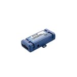
Dimensions of the product
Look and dimensions of the module are shown below. The module is mounted directly to the rail in the DIN industry standard. Power connectors, communication and IOs are at the bottom and top of the module. USB connector configuration and indicators located on the front of the module.
Communication configuration
Grounding and shielding
In most cases, IO modules will be installed in an enclosure along with other devices which generate electromagnetic radiation. Examples of these devices are relays and contactors, transformers, motor controllers etc. This electromagnetic radiation can induce electrical noise into both power and signal lines, as well as direct radiation into the module causing negative effects on the system. Appropriate grounding, shielding and other protective steps should be taken at the installation stage to prevent these effects. These protective steps include control cabinet grounding, module grounding, cable shield grounding, protective elements for electromagnetic switching devices, correct wiring as well as consideration of cable types and their cross sections.
Network Termination
Transmission line effects often present a problem on data communication networks. These problems include reflections and signal attenuation.
To eliminate the presence of reflections from the end of the cable, the cable must be terminated at both ends with a resistor across the line equal to its characteristic impedance. Both ends must be terminated since the direction of propagation is bi-directional. In the case of an RS485 twisted pair cable this termination is typically 120 Ω.
Setting Module Address in RS485 Modbus Network
The following table shows how to set switch to determine the address of the module. The module address is set with the switches in the range of 0 to 127. Addresses From 128 to 255 can by set via RS485 or USB.
| Adr | SW5 | SW4 | SW3 | SW2 | SW1 |
| 0 | OFF | OFF | OFF | OFF | OFF |
| 1 | OFF | OFF | OFF | OFF | ON |
| 2 | OFF | OFF | OFF | ON | OFF |
| 3 | OFF | OFF | OFF | ON | ON |
| 4 | OFF | OFF | ON | OFF | OFF |
| 5 | OFF | OFF | ON | OFF | ON |
| 6 | OFF | OFF | ON | ON | OFF |
| 7 | OFF | OFF | ON | ON | ON |
| 8 | OFF | ON | OFF | OFF | OFF |
| 9 | OFF | ON | OFF | OFF | ON |
| 10 | OFF | ON | OFF | ON | OFF |
| 11 | OFF | ON | OFF | ON | ON |
| 12 | OFF | ON | ON | OFF | OFF |
| 13 | OFF | ON | ON | OFF | ON |
| 14 | OFF | ON | ON | ON | OFF |
| 15 | OFF | ON | ON | ON | ON |
| 16 | ON | OFF | OFF | OFF | OFF |
| 17 | ON | OFF | OFF | OFF | ON |
| 18 | ON | OFF | OFF | ON | OFF |
| 19 | ON | OFF | OFF | ON | ON |
| 20 | ON | OFF | ON | OFF | OFF |
| 21 | ON | OFF | ON | OFF | ON |
| 22 | ON | OFF | ON | ON | OFF |
| 23 | ON | OFF | ON | ON | ON |
| 24 | ON | ON | OFF | OFF | OFF |
| 25 | ON | ON | OFF | OFF | ON |
| 26 | ON | ON | OFF | ON | OFF |
| 27 | ON | ON | OFF | ON | ON |
| 28 | ON | ON | ON | OFF | OFF |
| 29 | ON | ON | ON | OFF | ON |
| 30 | ON | ON | ON | ON | OFF |
| 31 | ON | ON | ON | ON | ON |
Types of Modbus Registers
There are 4 types of variables available in the module.
| Type | Beginning adress | Variable | Access | Modbus Command |
| 1 | 00001 | Digital Outputs | Bit
Read & Write |
1, 5, 15 |
| 2 | 10001 | Digital Inputs | Bit Read | 2 |
| 3 | 30001 | Input Registers | Registered Read | 3 |
| 4 | 40001 | Output Registers | Registered Read & Write | 4, 6, 16 |
Communication settings
The data stored in the modules memory are in 16-bit registers. Access to registers is via MODBUS RTU or MODBUS ASCII.
Default settings
You can restore the default configuration by the switch SW6 (see 3.5.2 – Restore the default configuration)
| Boud rate | 19200 |
| Pariti | None |
| Data bits | 1 |
| Reply Delay [ms] | 0 |
| Modbus Type | RTU |
| Boud rate | 19200 |
Restore the default configuration
To restore the default configuration:
- turn off the power
- turn on the switch SW6
- turn on the power
- when power and communication LED flash turn off the switch SW6
Caution! After restoring the default configuration all values stored in the registers will be cleared as well.
Configuration registers
| Modbus | Dec | Hex | Name | Values |
|
40003 |
2 |
0x02 |
Baud rate |
0 – 2400
1 – 4800 2 – 9600 3 – 19200 4 – 38400 5 – 57600 6 – 115200 other – value * 10 |
|
40005 |
4 |
0x04 |
Parity |
0 – none
1 – odd 2 – even 3 – always 1 4 – always 0 |
| 40004 | 3 | 0x03 | Stop Bits LSB | 1 – one stop bit 2 – two stop bit |
| 40004 | 3 | 0x03 | Data Bits MSB | 7 – 7 data bits
8 – 8 data bits |
| 40006 | 5 | 0x05 | Response delay | Time in ms |
| 40007 | 6 | 0x06 | Modbus Mode | 0 – RTU
1 – ASCII |
Watchdog function
This 16-bit register specifies the time in milliseconds to watchdog reset. If module does not receive any valid message within that time, all Digital and Analog Outputs will be set to the default state.
This feature is useful if there is an interruption in data transmission and for security reasons. Output states must be set to the appropriate state in order to assure the safety of persons or property.
The default value is 0 milliseconds which means the watchdog function is disabled.
Range: 0-65535 ms
Indicators

| Indicator | Description |
| Power supply | LED indicates that the module is correctly powered. |
| Communication | The LED lights up when the unit received the correct packet and sends the answer. |
| Inputs state | LED indicates that on the input is high state. |
| Outputs state | LED indicates that the output is on. |
Module Connection

Switches

| Switch | Function | Description |
| 1 | Module address +1 | Setting module address from 0 to 31 |
| 2 | Module address +2 | |
| 3 | Module address +4 | |
| 4 | Module address +8 | |
| 5 | Module address +16 | |
| 6 | Restoring default settings | Restoring default settings (see 3.5.1 – Default settings i 3.5.2 – Restore the default configuration). |
Modules Registers
Registered access
| Modbus | Dec | Hex | Register Name | Access | Description |
| 30001 | 0 | 0x00 | Version/Type | Read | Version and Type of the device |
| 30002 | 1 | 0x01 | Switches | Read | Switches state |
| 40003 | 2 | 0x02 | Baud rate | Read & Write | RS485 baud rate |
| 40004 | 3 | 0x03 | Stop Bits & Data Bits | Read & Write | No of Stop bits & Data Bits |
| 40005 | 4 | 0x04 | Parity | Read & Write | Parity bit |
| 40006 | 5 | 0x05 | Response Delay | Read & Write | Response delay in ms |
| 40007 | 6 | 0x06 | Modbus Mode | Read & Write | Modbus Mode (ASCII or RTU) |
| 40009 | 8 | 0x08 | Watchdog | Read & Write | Watchdog |
| 40013 | 12 | 0x0C | Default Output State | Read & Write | Default output state (after power on or watchdog reset) |
| 40018 | 17 | 0x11 | Inputs filter | Read & Write | Configuration of the inputs filter |
| 40033 | 32 | 0x20 | Received packets LSB | Read & Write |
No of received packets |
| 40034 | 33 | 0x21 | Received packets MSB | Read & Write | |
| 40035 | 34 | 0x22 | Incorrect packets LSB | Read & Write |
No of received packets with error |
| 40036 | 35 | 0x23 | Incorrect packets MSB | Read & Write | |
| 40037 | 36 | 0x24 | Sent packets LSB | Read & Write |
No of sent packets |
| 40038 | 37 | 0x25 | Sent packets MSB | Read & Write | |
| 30051 | 50 | 0x32 | Inputs | Read | Inputs state |
| 40052 | 51 | 0x33 | Outputs | Read & Write | Output state |
| 40053 | 52 | 0x34 | Counter 1 LSB | Read & Write |
32-bit counter 1 |
| 40054 | 53 | 0x35 | Counter 1 MSB | Read & Write | |
| 40055 | 54 | 0x36 | Counter 2 LSB | Read & Write |
32-bit counter 2 |
| 40056 | 55 | 0x37 | Counter 2 MSB | Read & Write | |
| 40057 | 56 | 0x38 | Counter 3 LSB | Read & Write |
32-bit counter 3 |
| 40058 | 57 | 0x39 | Counter 3 MSB | Read & Write | |
| 40059 | 58 | 0x3A | Counter 4 LSB | Read & Write |
32-bit counter 4 |
| 40060 | 59 | 0x3B | Counter 4 MSB | Read & Write | |
| 40061 | 60 | 0x3C | Counter 5 LSB | Read & Write |
32-bit counter 5 |
| 40062 | 61 | 0x3D | Counter 5 MSB | Read & Write | |
| 40063 | 62 | 0x3E | Counter 6 LSB | Read & Write |
32-bit counter 6 |
| 40064 | 63 | 0x3F | Counter 6 MSB | Read & Write | |
| 40065 | 64 | 0x40 | Counter 7 LSB | Read & Write |
32-bit counter 7 |
| 40066 | 65 | 0x41 | Counter 7 MSB | Read & Write | |
| 40067 | 66 | 0x42 | Counter 8 LSB | Read & Write | 32-bit counter 8 |
| Modbus | Dec | Hex | Register Name | Access | Description |
| 40068 | 67 | 0x43 | Counter 8 MSB | Read & Write | |
| 40085 | 84 | 0x54 | CCounter 1 LSB | Read & Write |
32-bit value of captured counter 1 |
| 40086 | 85 | 0x55 | CCounter 1 MSB | Read & Write | |
| 40087 | 86 | 0x56 | CCounter 2 LSB | Read & Write |
32-bit value of captured counter 2 |
| 40088 | 87 | 0x57 | CCounter 2 MSB | Read & Write | |
| 40089 | 88 | 0x58 | CCounter 3 LSB | Read & Write |
32-bit value of captured counter 3 |
| 40090 | 89 | 0x59 | CCounter 3 MSB | Read & Write | |
| 40091 | 90 | 0x5A | CCounter 4 LSB | Read & Write |
32-bit value of captured counter 4 |
| 40092 | 91 | 0x5B | CCounter 4 MSB | Read & Write | |
| 40093 | 92 | 0x5C | CCounter 5 LSB | Read & Write |
32-bit value of captured counter 5 |
| 40094 | 93 | 0x5D | CCounter 5 MSB | Read & Write | |
| 40095 | 94 | 0x5E | CCounter 6 LSB | Read & Write |
32-bit value of captured counter 6 |
| 40096 | 95 | 0x5F | CCounter 6 MSB | Read & Write | |
| 40097 | 96 | 0x60 | CCounter 7 LSB | Read & Write |
32-bit value of captured counter 7 |
| 40098 | 97 | 0x61 | CCounter 7 MSB | Read & Write | |
| 40099 | 98 | 0x62 | CCounter 8 LSB | Read & Write |
32-bit value of captured counter 8 |
| 40100 | 99 | 0x63 | CCounter 8 MSB | Read & Write | |
| 40117 | 116 | 0x74 | Counter Config 1 | Read & Write |
Counter Configuration
+1 – time measurement (if 0 counting impulses) +2 – autocatch counter every 1 sec +4 – catch value when input low +8 – reset counter after catch +16 – reset counter if input low +32 – encoder (only for counter 1 and 3) |
| 40118 | 117 | 0x75 | Counter Config 2 | Read & Write | |
| 40119 | 118 | 0x76 | Counter Config 3 | Read & Write | |
| 40120 | 119 | 0x77 | Counter Config 4 | Read & Write | |
| 40121 | 120 | 0x78 | Counter Config 5 | Read & Write | |
| 40122 | 121 | 0x79 | Counter Config 6 | Read & Write | |
| 40123 | 122 | 0x7A | Counter Config 7 | Read & Write | |
| 40124 | 123 | 0x7B | Counter Config 8 | Read & Write | |
| 40133 | 132 | 0x84 | Catch | Read & Write | Catch counter |
| 40134 | 133 | 0x85 | Status | Read & Write | Captured counter |
Bit access
| Adres Modbus | Adres Dec | Adres Hex | Nazwa rejestru | Dostęp | Opis |
| 193 | 192 | 0x0C0 | Default state of output 1 | Read & Write | Default state of output 1 |
| 194 | 193 | 0x0C1 | Default state of output 2 | Read & Write | Default state of output 2 |
| 195 | 194 | 0x0C2 | Default state of output 3 | Read & Write | Default state of output 3 |
| 196 | 195 | 0x0C3 | Default state of output 4 | Read & Write | Default state of output 4 |
| 197 | 196 | 0x0C4 | Default state of output 5 | Read & Write | Default state of output 5 |
| 198 | 197 | 0x0C5 | Default state of output 6 | Read & Write | Default state of output 6 |
| 199 | 198 | 0x0C6 | Default state of output 7 | Read & Write | Default state of output 7 |
| 200 | 199 | 0x0C7 | Default state of output 8 | Read & Write | Default state of output 8 |
| 10801 | 800 | 0x320 | Input 1 | Read | Input 1 state |
| 10802 | 801 | 0x321 | Input 2 | Read | Input 2 state |
| 10803 | 802 | 0x322 | Input 3 | Read | Input 3 state |
| 10804 | 803 | 0x323 | Input 4 | Read | Input 4 state |
| 10805 | 804 | 0x324 | Input 5 | Read | Input 5 state |
| 10806 | 805 | 0x325 | Input 6 | Read | Input 6 state |
| 10807 | 806 | 0x326 | Input 7 | Read | Input 7 state |
| 10808 | 807 | 0x327 | Input 8 | Read | Input 8 state |
| 817 | 816 | 0x330 | Output 1 | Read & Write | Output 1 state |
| 818 | 817 | 0x331 | Output 2 | Read & Write | Output 2 state |
| 819 | 818 | 0x332 | Output 3 | Read & Write | Output 3 state |
| 820 | 819 | 0x333 | Output 4 | Read & Write | Output 4 state |
| 821 | 820 | 0x334 | Output 5 | Read & Write | Output 5 state |
| 822 | 821 | 0x335 | Output 6 | Read & Write | Output 6 state |
| 823 | 822 | 0x336 | Output 7 | Read & Write | Output 7 state |
| 824 | 823 | 0x337 | Output 8 | Read & Write | Output 8 state |
| 2113 | 2112 | 0x840 | Capture 1 | Read & Write | Capture counter 1 |
| 2114 | 2113 | 0x841 | Capture 2 | Read & Write | Capture counter 2 |
| 2115 | 2114 | 0x842 | Capture 3 | Read & Write | Capture counter 3 |
| 2116 | 2115 | 0x843 | Capture 4 | Read & Write | Capture counter 4 |
| 2117 | 2116 | 0x844 | Capture 5 | Read & Write | Capture counter 5 |
| 2118 | 2117 | 0x845 | Capture 6 | Read & Write | Capture counter 6 |
| 2119 | 2118 | 0x846 | Capture 7 | Read & Write | Capture counter 7 |
| 2120 | 2119 | 0x847 | Capture 8 | Read & Write | Capture counter 8 |
| 2129 | 2120 | 0x848 | Captured 1 | Read & Write | Captured value of counter 1 |
| 2130 | 2129 | 0x849 | Captured 2 | Read & Write | Captured value of counter 2 |
| 2131 | 2130 | 0x84A | Captured 3 | Read & Write | Captured value of counter 3 |
| 2132 | 2131 | 0x84B | Captured 4 | Read & Write | Captured value of counter 4 |
| 2133 | 2132 | 0x84C | Captured 5 | Read & Write | Captured value of counter 5 |
| 2134 | 2133 | 0x84D | Captured 6 | Read & Write | Captured value of counter 6 |
| 2135 | 2134 | 0x84E | Captured 7 | Read & Write | Captured value of counter 7 |
| 2136 | 2135 | 0x84F | Captured 8 | Read & Write | Captured value of counter 8 |
Configuration software
Modbus Configurator is software that is designed to set the module registers responsible for communication over Modbus network as well as to read and write the current value of other registers of the module. This program can be a convenient way to test the system as well as to observe real-time changes in the registers.
Communication with the module is done via the USB cable. The module does not require any drivers.

Configurator is a universal program, whereby it is possible to configure all available modules.

ampero@ampero.eu
www.ampero.eu
Tel. +48 58 351 39 89; +48 58 732 71 73
Documents / Resources
 |
aspar RS485 8 Analogue Universal Inputs Module [pdf] User Manual RS485, 8 Analogue Universal Inputs, Universal Inputs, 8 Analogue Inputs, Inputs, RS485 8 Analogue Universal Inputs Module, 8 Analogue Universal Inputs Module |
 |
aspar RS485 8 Analogue Universal Inputs Module [pdf] User Manual RS485 8 Analogue Universal Inputs Module, RS485, 8 Analogue Universal Inputs Module, Universal Inputs Module |