SInBOn WSM-A0x Wi SUN Module
Wi‐SUN Introduction
Wi‐SUN is a wireless communication technology designed for large‐scale outdoor industrial and utility applications. It provides a reliable, secure, and low‐power solution for connecting devices in smart grid, smart city, and other Internet of Things (IoT) deployments. Wi‐SUN is based on the IEEE 802.15.4g standard and operates in the Sub‐GHz frequency range, which offers excellent propagation characteristics and long‐ rang connectivity.
Wi‐SUN Module Scope
The VC7300‐series (Vet ExCom SoC Solution) is a highly integrated wireless MCU that perfectly fits IoT networking and sensing applications. It integrates Cortex‐M3 MCU, 512/1024 KB Flash, 128 KB SRAM, sub‐GHz radio, and other functionalities such as UART/SPI/I2C, WDT, and Timer, etc.
The VC7300‐series has varieties of power‐saving modes which can be leveraged to build ultra‐low‐ power IoT networks with powerful computing capability. The embedded sub‐GHz RF transceiver features low power consumption, long‐range and robust wireless links, being able to reject large nearby interfering RF signals.
Furthermore, our module is designed to integrate with existing IP‐based networks, leveraging IPv6 protocols for seamless connectivity with the broader Internet. This enables the integration of Wi‐ SUN networks into larger smart grid and smart city deployments, facilitating efficient data collection, management, and control.
Application and Scenario
Smart Grid: Wi‐SUN enables efficient and secure communication between various components of a smart grid, such as smart meters, distribution automation devices, and grid management systems. It supports advanced metering infrastructure (AMI) and facilitates demand response, grid optimization, and distributed energy resource management.
Smart City: Wi‐SUN can be used for various applications in smart cities, including street lighting control, parking management, environmental monitoring, and infrastructure management. It provides a reliable and scalable communication platform to connect a wide range of devices and sensors deployed throughout the city.
Industrial Automation: Wi‐SUN offers robust wireless connectivity for industrial automation applications, such as asset tracking, remote monitoring, and control of equipment, and process optimization. It can be deployed in manufacturing plants, oil and gas facilities, and other industrial environments.
Advanced Metering Infrastructure (AMI): Wi‐SUN is well‐suited for AMI deployments, where it enables two‐way communication between utility companies and smart meters. It facilitates automated meter reading, remote disconnect/reconnect, and real‐time data collection for billing and load management.
Renewable Energy Integration: Wi‐SUN can play a crucial role in integrating renewable energy sources into the grid. It enables communication and control between renewable energy generation systems, energy storage devices, and the utility grid, allowing for efficient utilization and management of renewable resources.
Water Management: Wi‐SUN can be applied in water management systems to
enable real‐time monitoring of water supply, leak detection, and efficient distribution.
It allows utilities to collect data from various sensors and devices deployed across the
water network, enabling proactive maintenance and conservation measures.
Infrastructure Monitoring: Wi‐SUN can be used for monitoring critical infrastructure, such as bridges, dams, and pipelines. It provides wireless connectivity for sensors and monitoring devices, allowing for early detection of structural issues, environmental conditions, and preventive maintenance.
Specification
Key Features
- Vert ExCom VC7300 SoC
- Support IEEE802.15.4g/WI‐SUN FAN
- Support Wireless M‐BUS
- Radio frequency: ISM bands: NCC: 920MHz ~ 925MHz, FCC : 902MHz ~ 928MHz, CE: 868MHz
- Modulation method: OOK, (G)FSK, 4(G)FSK and GMSK
- Configurable maximum transmit output power : +20dBm
- Interface Support: UART/I2C/SPI/ADC/GPIO
- Root & Node (Dual application)
Characteristic specifications
| Parameter | Description |
| Radio standards | Compliant with IEEE802.15.4g/WI‐SUN |
| Radio frequency | NCC: 920MHz ~ 925MHz, FCC : 902MHz ~ 928MHz, CE: 868MHz |
| Modulation method | (G)FSK |
| Data rate | 50kbps |
| Receiving sensitivity | ‐109 dBm at 50 kbps GFSK (Typ.)(100 kbps,BER<0.1%) |
| Frequency deviation | ±20ppm or less |
| Power Supply | VDD=2.7~3.6V |
| Current consumption (VDD=3.3V)
(Data rate=100 kbps) |
50~145 mA(Typ.)[Transmission] 30 mA(Typ.)[Reception] 7mA(Typ.)[Sleep state] |
| Host interface | UART(115,200 bps) |
| Certification | FCC/CE/NCC |
Main Chip Diagram

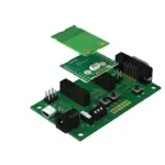
Module Diagram

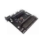
Module Pin Out
| PIN No. | Pin Name | I/O | Function |
| 1 | RFGPIO1 | 0 | RF Part general purpose Out (LNA_EN) |
|
2 |
BOOT |
I |
Default: General purpose IO, IOD0 Boot strap pin
0: Embedded flash boot. 1: Internal ROM boot. |
| 3 | RXD1 | I |
Debug/Programming |
| 4 | TXD1 | O | |
| 5 | TXD0 | O |
Application port |
| 6 | RXD0 | I | |
|
7 |
IOA7 |
I/O |
Default: General purpose IO, IOA7 Function 2: EINT7
Function 4: Second pulse output (RTC PCLK divider output) |
|
8 |
IOA6 |
I/O |
Default: General purpose IO, IOA6 Function 2: EINT6
Function 3: Comparator 2 output. Function 4: Key scan input 2 |
|
9 |
IOA4 |
I/O |
Default: General purpose IO, IOA4 Function 1: Comparator 2 P input
Function 2: EINT4 Function 4: Key scan input 0 |
| 10 | RESETN | I | External reset pin, low active. |
| 11 | GND | G | GND |
| 12 | VDD33 | P | DC Power |
| 13 | IOE4/ADC | I/O | Default: General purpose IO, IOE4. Function 1: ADC channel 4 input |
|
14 |
IOE5/ADC |
I/O |
Default: General purpose IO, IOE5
Function 1: ADC channel 5 input Function 2: VDCIN input |
| 15 | IOE6/ADC | I/O | Default: General purpose IO, IOE6. Function 1: ADC channel 6 input |
| 16 | IOE7/ADC | I/O | Default: General purpose IO, IOE7. Function 1: ADC channel 7 input |
| 17 | IOA0/SWCLK | I/O | Default: General purpose IO, IOA0 (MODE=1), SWCK(MODE=0). Function 2: EINT0 |
| 18 | IOA1/SWIO | I/O | Default: General purpose IO, IOA1 (MODE=1), SWIO(MODE=0). Function 2: EINT1 |
| 19 | GND | G | GND |
|
20 |
MODE |
I |
Debug mode or normal mode selection 0: Debug mode
1: Normal mode The signal level of this pin should be the same as DVDD33, and the state of this IO should not change during normal or debug operation. |
| 21 | IOA2 | I/O | Default: General purpose IO, IOA2. Function 2: EINT2 |
|
22 |
IOA3 |
I/O |
Default: General purpose IO, IOA3.
Function 1: Second pulse output (RTCPLL divider output) Function 2: EINT3 |
|
23 |
IOA9 |
I/O |
Default: General purpose IO, IOA9. Function 1: ADC channel 1 input
Function 2: EINT9 |
| PIN No. | Pin Name | I/O | Function |
|
24 |
IOB7/TXD5 |
I/O |
Default: General purpose IO, IOB7. Function 3: UART TXD 5
Function 5: FSPI HOLDN |
|
25 |
IOB1/RXD5 |
I/O |
Default: General purpose IO, IOB1.
Function 2: RTC Second pulse output (Correct in every 30 seconds) Function 3: UART RXD 5 Function 5: FSPI WPN |
|
26 |
IOB6/TXD4 |
I/O |
Default: General purpose IO, IOB6. Function 2: PWM1 output Function 3: UART TXD 4
Function 4: RTCLK clock output |
|
27 |
IOB0/RXD4 |
I/O |
Default: General purpose IO, IOB0.
Function 2: PWM0 output Function 3: UART RXD 4 |
|
28 |
IOB15/EXT_CLK |
I/O |
Default: General purpose IO, IOB15. Function 2: Timer external clock input Function 3: UART RXD 6
Function 4: Key‐scan output 3 Function 5: FSPI flash CSN |
|
29 |
IOB14/PWM/SD |
I/O |
Default: General purpose IO, IOB14. Function 2: PWM3 output
Function 3: I2C SDA Function 4: Key scan output 2 |
|
30 |
IOB13/PWM/SCL |
I/O |
Default: General purpose IO, IOB13. Function 2: PWM2 output
Function 3: I2C SCL Function 4: Key scan output 1 |
|
31 |
IOB12/MOSI |
I/O |
Default: General purpose IO, IOB12. Function 2: SPI1 MOSI
Function 5: FSPI MOSI |
|
32 |
IOB11/MISO |
I/O |
Default: General purpose IO, IOB11. Function 2: SPI1 MISO
Function 5: FSPI MISO |
|
33 |
IOB10/CLK |
I/O |
Default: General purpose IO, IOB10. Function 2: SPI1 CLK
Function 5: FSPI CLK |
|
34 |
IOB9/F_CS |
I/O |
Default: General purpose IO, IOB9. Function 2: SPI1 CSN
Function 5: FSPI flash CSN |
|
35 |
IOB8/S_CS |
I/O |
Default: General purpose IO, IOB8.
Function 4: Key scan output 0 Function 5: FSPI SRAM CSN |
| 36 | GND | G | GND |
| 37 | TXO_M_OUT | O | EXT PA, RF single out |
| 38 | GND | G | GND |
| 39 | GND | GND | GND |
| 40 | TXO_M_IN | I | EXT PA, RF single in |
| 41 | GND | GND | GND |
| 42 | GPIO5 | I/O | GPIO we PA Power Control |
| 43 | GND | GND | GND |
| 44 | ANT | RF | RF in /out |
| 45 | GND | GND | GND |
Suggested circuit

Module PCB Dimension

Environmental
| Item | Specifications |
| Operating Temperature Range | ‐40~85℃ |
| Operating Humidity Range | 20 to 90% RH (without condensation or freezing) |
| Storage Temperature Range | ‐40~105℃ |
| Storage Operating Humidity Range | 20 to 95% RH
(Sharp temperature change, without condensation or freezing not allowed) |
Recommended Land Pattern

Odering and Marking Information
| Part Number | Description | Note |
| WSM‐A01 | IEEE 802.15.4g, Wi‐SUN Stamp Module , LPWAN, U.FLx1 (915Mhz) | A9314288‐001 |
| WSM‐A02 | IEEE 802.15.4g, Wi‐SUN Stamp Module , LPWAN, U.FLx1 (868Mhz) | TBC |
Product Marking

Packing Information

AFEDERAL COMMUNICATIONS COMMISSION INTERFERENCE STATEMENT
This equipment has been tested and found to comply with the limits for a Class B digital device, pursuant to part 15 of the FCC Rules. These limits are designed to provide reasonable protection against harmful interference in a residential installation. This equipment generates, uses and can radiate radio frequency energy and, if not installed and used in accordance with the instructions, may cause harmful interference to radio communications. However, there is no guarantee that interference will not occur in a particular installation. If this equipment does cause harmful interference to radio or television reception, which can be determined by turning the equipment off and on, the user is encouraged to try to correct the interference by one or more of the following measures:
- Reorient or relocate the receiving antenna.
- Increase the separation between the equipment and receiver.
- Connect the equipment into an outlet on a circuit different from that to which the receiver is connected.
- Consult the dealer or an experienced radio/ TV technician for help.
CAUTION:
Any changes or modifications not expressly approved by the grantee of this device could void the user’s authority to operate the equipment.
authority to operate the equipment.
(Section 15.19)(a)(3) This device complies with Part 15 of the FCC Rules. Operation is subject to the following two conditions:
(1) this device may not cause harmful interference, and (2) this device must accept any interference received, including interference that may cause undesired operation.
This transmitter module is authorized only for use in device where the antenna may be installed such that 20cm may be maintained between the antenna and users. The final end product must be labeled in a visible area with the following: “Contains FCC ID: XXXXX‐XXXXX”.
Information for the OEMs and Integrators:
This device is intended only for OEM integrators under the following conditions:
The module can be used to installation in other host.
the transmitter module may not be collocated with any other transmit or antenna. The module shall be only used with the integral antenna(s) that has been originally tested and certified with this module. As long as 2 conditions above are met, further transmitter test will not be required. However, the OEM integrator is still responsible for testing their end‐product for any additional compliance requirement with this module installed (for example, digital device emission, PC peripheral requirements, etc.)
The final end product must be labeled in a visible area with the following: ” FCC ID: XXXXX‐XXXXX”. The equipment complies with FCC RF exposure limits set forth for an uncontrolled environment. The equipment must not be co‐located or operating in conjunction with any other antenna or transmitter.

Documents / Resources
 |
SInBOn WSM-A0x Wi SUN Module [pdf] User Manual SLB-WSM, SLBWSM, WSM-A0x, WSM A0x Wi SUN Module, Wi SUN Module, SUN Module, Module |