Nexcom International Co., Ltd.
10F, No.920, Chung-Cheng Road
Zhonghe Dist., New Taipei City
Taiwan 235, R.O.C
Bluetooth LE Module
MD88SFA
Version Note
| Version | Details | Contributor(s) | Date | Notes |
| 1.0.0 | First edit | Michelle, Leo | 2024.05.09 | |
Part Number
| Model | Hardware Code |
| MS88SFA8 | 8Y33AI| |
MS88SFA-nRF52833
___
Low Power, Multi-Protocol Bluetooth 5.4 PA Module
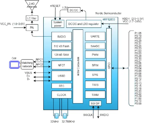
The MS88SFA is a BLES.4 PA/LNA module base on Nighty flexible and very low power-loss nRFS2833 SoC. It owns o RF transceiver of Cortex-M4F ARM core operating at speed of 64Mhz. Besides. it has 512kB FLASH programmer space. 128kB RAM and other matching powerful resources. The nRF52833 is able to support ANT. BLE. BLE MESH. ZIGBEE and THREAD protocols. etc. Communication distance up to 600m under condition of 1Mbps rote and PA/LNA built in.
FEATURES
___
 Bluetooth 5.4
 Built-in PA/LNA
 Power up to Maximurn+20dbm
 Support ANT, BLE, BLE MESH, ZIGBEE and THREAD protocols, etc.
 Transmission distance up to 600 meters in open space
KEY PARAMETER
___
MS88SFA-nRF52833
| Chip Model | Nordic nRF52833 |
| Module Site | 23.2×17.4×2mm |
| Flash | 512kB |
| Receiving Sensitivity | -96dBm |
| Antenna | APEX(MHF 5) |
| GPIO | 29 |
| RAM | 128KB |
| Transmission Power | ~+20dBm |
1 BLOCK DIAGRAM
___
2 ELECTRICAL SPECIFICATION
___
| Parameters | Value | Notes |
| Working Voltage | 1.7V-5.5V | To ensure RF work, supply voltage suggest not lower than 3V |
| Working Temperature | -40 °C ~+85 °C | Storage temperature is -40 °C ~+125 °C |
| Transmission Power | ~+20dBrn | Configurable |
| Module Dimension | 23.2*17.4*2mm | |
| Quantity of IO Port | 29 |
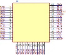
3 PIN DESCRIPTION
___
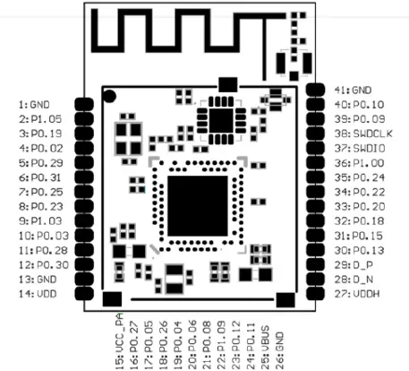
4 PIN DEFINITION
___
| Pin Number | Symbol | Type | Definition |
| 14 | VDD | Power source | Power supply: 1.7V-3.6V, short-circuit VDD and VDDH to use the pin to supply power |
| 27 | VDDH | Power source | Power supply 2.5V-5.5V; When supply 5V electricity, use this pin to supply power, not connect vin pin. |
| 1/13/26/41 | GND | Ground | Ground |
| 37/38 | SWCLK/ SWDIO | Debug | Debug, when debugging only need to connect power supply pin, ground and these 2 pins. |
| 2-12/16-24/30-36/39-40 | P0.02-P0.31 P1.00-P1.09 |
I/O | IO port for general purpose |
| 25 | VBUS | Power source for USB port | 5V input current for USB 3.3V modulator Need to supply 5V current and short-circuit this pi with VDDH When use USB port |
| 15 | VCC_PA | PA supply power pin | Must provide electricity of 2.7-3.6V stably, 1.7V-3.6V chip voltage, this pin can be shorted to VDD/VDDH |
| 29 | D+ | Digital interfaces | USB D+ |
| 28 | D- | Digital interfaces | USB D- |
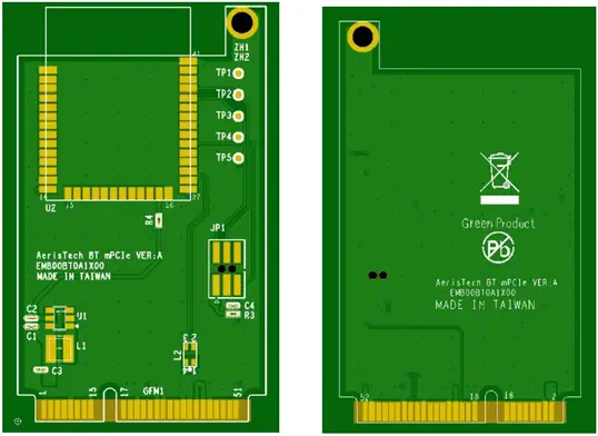
5 MECHANICAL DRAWING
___

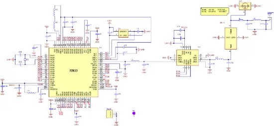
6 ELECTRICAL SCHEMATIC
___
| TXEN | RXEN | MODE | Operational Mode |
| 0 | 0 | 0 | Shutdown mode |
| 0 | 1 | 0 | Rx High Current/Low NF Mode |
| 1 | 0 | 0 | TX Mode |
| 1 | 1 | 0 | TX Mode |
| 0 | 0 | 1 | Bypass Mode |
| 0 | 1 | 1 | Rx Low Current Mode |
![]() Notice: Before placing an order, please confirm the specific configuration required with the salesperson.
Notice: Before placing an order, please confirm the specific configuration required with the salesperson.
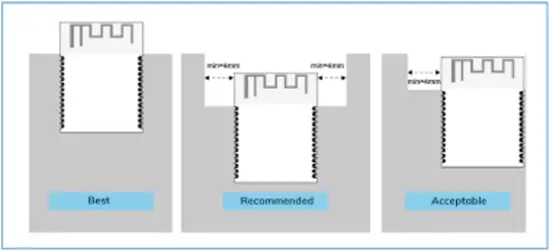
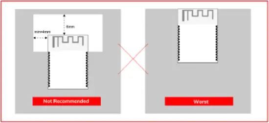
7 PCB LAYOUT
___
There should be no GND plane or metal cross wiring in the module antenna area, and components should not be placed nearby. It is best to make a hollow or clear area, or place it on the edge of the PCB board.
![]() Notice: Refer to examples as below, and highly suggest to use the first design and the adjustment of modules antenna design according to the first wiring.
Notice: Refer to examples as below, and highly suggest to use the first design and the adjustment of modules antenna design according to the first wiring.
Layout Notes:
1) Preferred Module antenna area completely clearance and not be prevented by metals, otherwise it will influence antenna’s effect (as above DWG. indication).
2) Cover the external part of module antenna area with copper as far as possible to reduce the main board’s signal cable and other disturbing.
3) It is preferred to have a clearance area of 4 square meter or more area around the module antenna (including the shell) to reduce the influence to antenna.
4) Device should be grounded well to reduce the parasitic inductance.
5) Do not cover copper under module’s antenna in order to avoid affect signal radiation or lead to transmission distance affected.
6) Antenna should keep far from other circuits to prevent radiation efficiency reduction or affects the normal operation of other lines.
7) Module should be placed on edge of circuit board and keep a distance away from other circuits.
8) Suggesting to use magnetic beads to insulate module’s access power supply.
8 REFLOW AND SOLDERING
___
1) Do SMT according to above reflow oven temperature deal curve. Max. Temperature is 260°C;
Refer to IPC/JEDEC standard; Peak TEMP<260 °C ; Times: ≤2 times, suggest only do once reflow soldering on module surface in case of SMT double pad involved. Contact us if special crafts involved.
2) Suggesting to make 0.2mm thickness of module SMT for partial ladder steel mesh. then make the opening extend 0.8mm
3) After unsealing, it cannot be used up at one time, should be vacuumed for storage, couldn’t be exposed in the air for long time. Please avoid getting damp and soldering-pan oxidizing. If there are 7 to 30 days interval before using online SMT, suggest to bake at 65-70 °C for 24 hours without disassembling the tape.
4) Before using SMT. please adopt ESD protection measure.

9. label
![]()
FCC ID: YHIMD88SFA
Model: MD88SFA
10 STORAGE CONDITIONS
___
- Please use this product within 6 months after signing the receipt.
– This product should be stored without opening the package at an ambient temperature of 5-35°C and a humidity of 20-70%RH.
– This product should be left for more than 6 months after receipt and should be confirmed before use.
– The product must be stored in a non-corrosive gas (Cl2, NH3, SO2, NOx, etc.).
– To avoid damaging the packaging material, do not apply any excessive mechanical shocks, including but not limited to sharp objects adhering to the packaging material and product dropping. - This product is suitable for MSL2 (based on JEDEC standard J-STD-020).
– After opening the package. the product must be stored at ≤30°C/<60%RH. It is recommended to use the product within 3-6 months after opening the package.
– When the color of the indicator in the package changes, the product should be baked before welding. - Baking is not required for one year if exposure is limited to <30°C and 60%RH. Refer to MSL2 for exposure criteria for moisture sensitivity level. If exposed to (≥168h©85°C/60%RH) conditions or stored for more than one year, recommended baking conditions.
1. 120 +5/-5°C, 8 hours, 1 time
Products must be baked individually on heat-resistant trays because the materials (base tape, reel tape. and cover tape) are not heat-resistant. and the packaging material may be deformed at temperatures of 120 °C;
2. 90°C +8/-0°C , 24hours, 1times
The base tape can be baked together with the product at this temperature. Please pay attention to the uniformity of heat.
11 HANDLING CONDITIONS
___
- Be careful in handling or transporting products because excessive stress or mechanical shock may break products.
- Handle with care if products may have cracks or damages on their terminals. If there is any such damage, the characteristics of products may change. Do not touch products with bare hands that may result in poor solder ability and destroy by static electrical charge.
12 QUALITY
___
Cognizant of our commitment to quality, we operate our own factory equipped with state-of-the-art production facilities and a meticulous quality management system. We hold certifications for ISO9001, ISO14001, ISO27001, OHSA18001, BSCI.
Every product undergoes stringent testing, including transmit power, sensitivity, power consumption, stability, and aging tests. Our fully automated module production line is now in full operation, boasting a production capacity in the millions, capable of meeting high-volume production demands.
13.
FEDERAL COMMUNICATIONS COMMISSION INTERFERENCE STATEMENT
This equipment has been tested and found to comply with the limits for a Class B digital device, pursuant to part 15 of the FCC Rules. These limits are designed to provide reasonable protection against harmful interference in a residential installation. This equipment generates, uses and can radiate radio frequency energy and, if not installed and used in accordance with the instructions, may cause harmful interference to radio communications.
However, there is no guarantee that interference will not occur in a particular installation. If this equipment does cause harmful interference to radio or television reception, which can be determined by turning the equipment off and on, the user is encouraged to try to correct the interference by one or more of the following measures:
-Reorient or relocate the receiving antenna.
-Increase the separation between the equipment and receiver.
-Connect the equipment into an outlet on a circuit different from that to which the receiver is connected.
-Consult the dealer or an experienced radio/ TV technician for help.
CAUTION:
Any changes or modifications not expressly approved by the grantee of this device could void the user’s authority to operate the equipment.
RF Exposure warning
This equipment must be installed and operated in accordance with provided instructions and the antenna(s) used for this transmitter must be installed to provide a separation distance of at least 20 cm from all persons and must not be co-located or operating in conjunction with any other antenna or transmitter. End-users and installers must be provide with antenna installation instructions and transmitter operating conditions for satisfying RF exposure compliance.
Information for OEMs and host integrators
The OEM or integrator is obligated to adhere to these requirements and restrictions as a condition for using the module’s certification.
The OEM or integrator is responsible to perform the required additional host regulatory testing and/or obtaining the required host approvals for compliance.
Per KDB 996369 D03 v01r01 OEM Manual section 2.2 to 2.12, this module is intended for OEM integrators under the following conditions:
2.2 List of applicable FCC rules
This module has been tested for compliance to FCC Part 15 Subpart C (15.247).
2.3 Summarize the specific operational use conditions
The module is tested for standalone mobile RF exposure use condition. Any other usage conditions such as colocation with other transmitter(s) will need a separate reassessment through a class II permissive change application or new certification.
2.4 Limited module procedures
Not applicable, this device is a single modular approval and meets FCC 47 CFR 15.212 requirement.
2.5 Trace antenna designs
Not applicable. This module should use an external antenna, and use of internal PCB antenna is prohibited. The module has been approved to operate with the antenna types listed below, with the maximum permissible gain indicated.
| No. | 1 |
| Manufacturer | ARISTOTLE |
| Part No. | RFA-25-T42-U-M70 |
| Antenna Type | OMNI |
| Peak Gain (dBi) | 2.6 dBi |
| Freq. Range (GHz) | 2.4~2.4835 |
| Connector Type | RP SMA PLUG |
2.6 RF exposure considerations
This equipment complies with FCC mobile radiation exposure limits set forth for an uncontrolled environment. This equipment should be installed and operated with a minimum distance of 20cm between the radiator & your body. A separate SAR/Power Density evaluation is required to confirm compliance with relevant FCC portable RF exposure rules.
2.7 Label and compliance information
Label of the end product:
The final end product must be labeled in a visible area with the following: “Contains FCC ID: YHIMD88SFA”. The grantee’s FCC ID can be used only when all FCC compliance requirements are met
2.8 Information on test modes and additional testing requirements
This transmitter is tested in a standalone mobile RF exposure condition and any co-located or simultaneous transmission with other transmitter(s) class II permissive change re-evaluation or new certification.
2.9 Additional testing, Part 15 Subpart B disclaimer
This transmitter module is tested as a subsystem and its certification does not cover the FCC Part 15 Subpart B (unintentional radiator) rule requirement applicable to the final host. The final host will still need to be reassessed for compliance to this portion of rule requirements if applicable. As long as all conditions above are met, further transmitter test will not be required. However, the OEM integrator is still responsible for testing their end-product for any additional compliance requirements required with this module installed.
IMPORTANT NOTE: In the event that these conditions cannot be met (for example certain laptop configurations or co-location with another transmitter), then the FCC authorization is no longer considered valid and the FCC ID cannot be used on the final product. In these circumstances, the OEM integrator will be responsible for reevaluating the end product (including the transmitter) and obtaining a separate FCC authorization.
Manual Information To the End User
The OEM integrator has to be aware not to provide information to the end user regarding how to install or remove this RF module in the user’s manual of the end product which integrates this module. The end user manual shall include all required regulatory information/warning as show in this manual.
OEM/Host manufacturer responsibilities
OEM/Host manufacturers are ultimately responsible for the compliance of the Host and Module. The final product must be reassessed against all the essential requirements of the FCC rule such as FCC Part 15 Subpart B before it can be placed on the US market. This includes reassessing the transmitter module for compliance with the Radio and EMF essential requirements of the FCC rules. This module must not be incorporated into any other device or system without retesting for compliance as multi-radio and combined equipment.
Warning message
This device complies with Part 15 of the FCC Rules. Operation is subject to the following two conditions: (1) this device may not cause harmful interference, and (2) this device must accept any interference received, including interference that may cause undesired operation.
Documents / Resources
 |
Nexcom MD88SFA Bluetooth LE Module [pdf] User Manual MD88SFA, YHIMD88SFA, md88sfa, MD88SFA Bluetooth LE Module, MD88SFA, Bluetooth LE Module, LE Module, Module |