![]()
LCUK54-WWD
Hardware Design
LTE-A Series
Version: 1.0.0
Date: 2024-04-01
Status: Preliminary
LCUK54-WWD Module
Our aim is to provide timely and comprehensive services to our customers. If you require any assistance, please contact our headquarters:
NetPrisma US INC.
100 N HOWARD ST STE R, SPOKANE, WA, 99201 Email: Info@netprisma.us
Or our local offices. For more information, please visit: https://www.netprisma.us/sales-support/.
For technical support, or to report documentation errors, please visit: https://www.netprisma.us/tech-support/. Or email us at: support@netprisma.us.
Legal Notices
We offer information as a service to you. The provided information is based on your requirements and we make every effort to ensure its quality. You agree that you are responsible for using independent analysis and evaluation in designing intended products, and we provide reference designs for illustrative purposes only. Before using any hardware, software or service guided by this document, please read this notice carefully. Even though we employ commercially reasonable efforts to provide the best possible experience, you hereby acknowledge and agree that this document and related services hereunder are provided to you on an “as available” basis. We may revise or restate this document from time to time at our sole discretion without any prior notice to you.
Use and Disclosure Restrictions
License Agreements
Documents and information provided by us shall be kept confidential, unless specific permission is granted. They shall not be accessed or used for any purpose except as expressly provided herein.
Copyright
Our and third-party products hereunder may contain copyrighted material. Such copyrighted material shall not be copied, reproduced, distributed, merged, published, translated, or modified without prior written consent. We and the third party have exclusive rights over copyrighted material. No license shall be granted or conveyed under any patents, copyrights, trademarks, or service mark rights. To avoid ambiguities, purchasing in any form cannot be deemed as granting a license other than the normal non-exclusive, royalty-free license to use the material. We reserve the right to take legal action for noncompliance with abovementioned requirements, unauthorized use, or other illegal or malicious use of the material.
Trademarks
Except as otherwise set forth herein, nothing in this document shall be construed as conferring any rights to use any trademark, trade name or name, abbreviation, or counterfeit product thereof owned by NetPrisma or any third party in advertising, publicity, or other aspects.
Third-Party Rights
This document may refer to hardware, software and/or documentation owned by one or more third parties (“third-party materials”). Use of such third-party materials shall be governed by all restrictions and obligations applicable thereto.
We make no warranty or representation, either express or implied, regarding the third-party materials, including but not limited to any implied or statutory, warranties of merchantability or fitness for a particular purpose, quiet enjoyment, system integration, information accuracy, and non-infringement of any third-party intellectual property rights with regard to the licensed technology or use thereof. Nothing herein constitutes a representation or warranty by us to either develop, enhance, modify, distribute, market, sell, offer for sale, or otherwise maintain production of any our products or any other hardware, software, device, tool, information, or product. We moreover disclaim any and all warranties arising from the course of dealing or usage of trade.
Privacy Policy
To implement module functionality, certain device data are uploaded to NetPrisma’s or third-party’s servers, including carriers, chipset suppliers or customer-designated servers. NetPrisma, strictly abiding by the relevant laws and regulations, shall retain, use, disclose or otherwise process relevant data for the purpose of performing the service only or as permitted by applicable laws. Before data interaction with third parties, please be informed of their privacy and data security policy.
Disclaimer
a) We acknowledge no liability for any injury or damage arising from the reliance upon the information.
b) We shall bear no liability resulting from any inaccuracies or omissions, or from the use of the information contained herein.
c) While we have made every effort to ensure that the functions and features under development are free from errors, it is possible that they could contain errors, inaccuracies, and omissions. Unless otherwise provided by valid agreement, we make no warranties of any kind, either implied or express, and exclude all liability for any loss or damage suffered in connection with the use of features and functions under development, to the maximum extent permitted by law, regardless of whether such loss or damage may have been foreseeable.
d) We are not responsible for the accessibility, safety, accuracy, availability, legality, or completeness of information, advertising, commercial offers, products, services, and materials on third-party websites and third-party resources.
Copyright © NetPrisma US 2024. All rights reserved.
Revision History
| Version | Date | Description |
| – | 2024-04-01 | Creation of the document |
| 1.0.0 | 2024-04-01 | Preliminary |
Introduction
This document defines LCUK54-WWD module and describes its air and hardware interfaces which are connected to your applications.
This document can help you quickly understand the interface specifications, electrical and mechanical details as well as other related information of the module. Besides, reference designs will be offered to exemplify diverse applications of the modules. With this hardware design coupled with application notes and user guides, you can use the module to design and set up mobile applications easily.
1.1. Reference Standard
The module complies with the following standards:
- PCI Express M.2 Specification Revision 4.0
- Universal Serial Bus Specification, Revision 4.0
- ISO/IEC 7816-3
- MIPI Alliance Specification for RF Front-End Control Interface Version 2.0
- 3GPP TS 27.007 and 3GPP TS 27.005
- 3GPP TS 34.121-1 and 3GPP TS 36.521-1
1.2. Special Marks
Table 1: Special Marks
| Mark | Definition |
|
* |
Unless otherwise specified, an asterisk (*) after a function, feature, interface, pin name, command, argument, and so on indicates that it is under development and currently not supported; and the asterisk (*) after a model indicates that the model sample is currently unavailable. |
| […] | Brackets ([…]) used after a pin enclosing a range of numbers indicate all pins of the same type. For example, SDIO_DATA[0:3] refers to all four SDIO pins: SDIO_DATA0, SDIO_DATA1, SDIO_DATA2, and SDIO_DATA3. |
Product Overview
2.1. Frequency Bands and Functions
LCUK54-WWD is an LTE-A/UMTS/HSPA+ wireless communication module with diversity receiver. It provides data connectivity on LTE-FDD, LTE-TDD, DC-HSDPA, HSPA+, HSDPA, HSUPA and WCDMA networks. It is standard WWAN M.2 Key-B module. For more details, see PCI Express M.2 Specification Revision 4.0.
It supports embedded operating systems such as Windows, Linux and Android, and also provides GNSS 1 to meet specific application demands.
The following table shows the frequency bands and GNSS functions of the module. For details about CA combinations, you can see document [1].
Table 2: Frequency Bands and GNSS Function
| Mode | Frequency Band |
| LTE-FDD (with Rx-diversity) | B1/B2/B3/B4/B5/B7/B8/B12/B13/B14/B17/B18/B19/B20/B25/B26 /B28/B29 2/B30/B32 2/B66/B71 |
| LTE-TDD (with Rx-diversity) | B34/B38/B39/B40*/B41/B42/B43/B46 2/B48 (CBRS) |
| WCDMA (with Rx-diversity) | B1/B2/B3/B4/B5/B6/B8/B19 |
*Note :B40 not for FCC/IC
2.2. Key Features
Table 3: Key Features
| Feature | Details |
| Function Interface | PCI Express M.2 Interface |
| Power Supply | • Supply voltage: 3.135–4.4 V • Typical supply voltage: 3.3 V |
| (U)SIM Interfaces | • Compliant with ISO/IEC 7816-3 and ETSI and IMT-2000 requirements • Supports (U)SIM card: 1.8/3.0 V • Supports Dual SIM Single Standby (one eSIM and one USIM interface) |
- GNSS function is optional.
- LTE-FDD B29/B32 and LTE-TDD B46 support Rx only and is only for secondary component carrier.
| eSIM | Optional eSIM function |
|
USB Interface |
• Reserves USB 3.0 interface • Compliant with USB 3.0 and 2.0 specifications, with maximum transmission rates up to 5 Gbps on USB 3.0 and 480 Mbps on USB 2.0 • Used for AT command communication, data transmission, firmware upgrade (USB 2.0 only), software debugging and GNSS NMEA sentence output • Supports USB serial drivers: – Windows 10/11 – Linux 2.6–6.x – Android 4.x–13.x |
| PCM Interface* (Reserved) | • Used for audio function through an external codec • Supports 16-bit linear data format • Supports long and short frame synchronization • Supports master and slave modes, but must be in master mode in long frame synchronization |
| PCIe Interface (Reserved) | • Compliant with PCI Express Base Specification Revision 2.0 • Supports one PCIe interface, up to 5 Gbps/lane • Used for data transmission • RC mode only |
| Rx-diversity | LTE/WCDMA |
| Antenna Interfaces | • Main antenna connector and diversity/GNSS antenna connector • 50 Ω impedance |
|
Transmitting Power |
• WCDMA: Class 3 (23 dBm ±2 dB) • LTE B7/B38/40/B41: Class 3 (23 dBm ±1 dB) • LTE B30: Class 3 (22 dBm ±1 dB) • LTE B42/B43/B48: Class 3 (21 dBm ±1 dB) • LTE other bands: Class 3 (23.5 dBm ±1 dB) |
| LTE Features | • Supports 3GPP Rel-12 LTE-FDD and LTE-TDD • LTE-FDD: Max. 300 Mbps (DL)/50 Mbps (UL) • LTE-TDD: Max. 226 Mbps (DL)/28 Mbps (UL) • Supports CA category: up to DL CA Cat 6 • Supports 1.4/3/5/10/15/20 MHz RF bandwidth • Supported modulations: – Downlink: QPSK, 16QAM and 64QAM modulations – Uplink: QPSK and 16QAM modulations |
| UMTS Features | • Supports 3GPP Rel-9 DC-HSDPA, HSPA+, HSDPA, HSUPA and WCDMA • Supported modulations: – Downlink: BPSK, QPSK, 16QAM and 64QAM modulations – Uplink: BPSK, QPSK • Maximum transmission data rates 3: – DC-HSDPA: 42 Mbps (DL) – HSUPA: 5.76 Mbps (UL) – WCDMA: 384 kbps (DL)/384 kbps (UL) |
| GNSS Features 3 | • Supports GPS, GLONASS, BDS, Galileo and QZSS • Data update rate: 1 Hz by default |
| AT Commands | • Compliant with 3GPP TS 27.007 and 3GPP TS 27.005 • Enhanced AT commands |
3 GNSS function is optional.
| Internet Protocol Features | Supports QMI/MBIM/NITZ/HTTP/HTTPS |
| Firmware Upgrade | • USB 2.0 • DFOTA |
| SMS | • Point-to-point MO and MT • Text and PDU modes • SMS cell broadcast • SMS storage: ME by default |
| Physical Characteristics | • M.2 Key-B • Size: 30.0 mm × 42.0 mm × 2.3 mm • Weight: approx. 6.2 g |
| Temperature Ranges | • Operating temperature range 4: -25 to +75 °C • Extended temperature range 5: -40 to +85 °C • Storage temperature range: -40 to +90 °C |
| RoHS | All hardware components are fully compliant with EU RoHS directive |
2.3. Functional Diagram
The following figure shows a functional diagram of LCUK54-WWD
- Power management
- Baseband
- LPDDR2 SDRAM + NAND flash
- Radio frequency
- M.2 Key-B interface
4 To meet the normal operating temperature range requirements, it is necessary to ensure effective thermal dissipation, e.g., by adding passive or active heat sinks, heat pipes, vapor chambers. Within the temperature range of -10 °C to +55 °C, the mentioned RF performance margins higher than 3GPP specifications can be guaranteed. When temperature goes beyond temperature range of -10 °C to +55 °C, a few RF performances of module may be slightly off 3GPP specifications.
5 To meet the extended operating temperature range requirements, it is necessary to ensure effective thermal dissipation, e.g., by adding passive or active heat sinks, heat pipes, vapor chambers. Within this range, the module remains the ability to establish and maintain functions such as SMS, without any unrecoverable malfunction. Radio spectrum and radio network are not influenced, while one or more specifications, such as Pout, may undergo a reduction in value, exceeding the specified tolerances of 3GPP. When the temperature returns to the normal operating temperature level, the module will meet 3GPP specifications again.

2.4. Pin Assignment
The following figure shows the pin assignment of the module.
NOTE
Before the module turns on, ensure the pins DPR and USIM_DET are not pulled high to avoid current sink damaging the module. For more details, contact NetPrisma Technical Support.
2.5. Pin Definitions
Table 4: Parameter Definition
| Parameter | Description |
| AI | Analog Input |
| AO | Analog Output |
| AIO | Analog Input/Output |
| DI | Digital Input |
| DO | Digital Output |
| DIO | Digital Input/Output |
| OD | Open Drain |
| PI | Power Input |
| PO | Power Output |
| PU | Pull Up |
| PD | Pull Down |
DC characteristics include power domain and rated current.
Table 5: Pin Description
| Pin No. | Pin Name | I/O | Description | DC Characteristics | Comment |
| 1 | CONFIG_3 | DO | Not connected internally | ||
| 2 | VCC | PI | Power supply for the module | Vmin = 3.135 V Vnom = 3.3 V Vmax = 4.4 V |
|
| 3 | GND | Ground | |||
| 4 | VCC | PI | Power supply for the module | Refer to Pin 2 | |
| 5 | GND | Ground | |||
| 6 | FULL_CARD_ POWER_OFF# | DI, PD | Turn on/off the module High level: turn on Low level: turn off | VIHmax = 4.4 V VIHmin = 1.19 V VILmax = 0.2 V | Internally pulled down with a 100 kΩ resistor. |
| 7 | USB_DP | AIO | USB differential data (+) | Require differential impedance of 90 Ω. A test point must be reserved. |
|
| 8 | W_DISABLE1# | DI | Airplane mode control Active LOW | 1.8/3.3 V | Internally pulled up to 1.8 V with a 100 kΩ resistor. |
| 9 | USB_DM | AIO | USB differential data (-) | Require differential impedance of 90 Ω. A test point must be reserved. |
| 10 | WWAN_LED# | OD | RF status LED indicator Active LOW | VCC | |
| 11 | GND | Ground | |||
| 12 | Notch | Notch | |||
| 13 | Notch | Notch | |||
| 14 | Notch | Notch | |||
| 15 | Notch | Notch | |||
| 16 | Notch | Notch | |||
| 17 | Notch | Notch | |||
| 18 | Notch | Notch | |||
| 19 | Notch | Notch | |||
| 20 | RESERVED | Reserved for PCM* clock | |||
| 21 | CONFIG_0 | DO | Connected to GND internally | ||
| 22 | RESERVED | Reserved for PCM* data input | |||
| 23 | WAKE_ON_WAN# | OD | Wake up the host Active LOW | 1.8/3.3 V | Externally pull up to 1.8 V or 3.3 V. |
| 24 | RESERVED | Reserved for PCM* data output | |||
| 25 | DPR | DI, PU | Dynamic power reduction Active LOW | 1.8 V | High level by default. |
| 26 | W_DISABLE2#* | Reserved for GNSS control | Internally pulled up to 1.8 V with a 100 kΩ resistor. | ||
| 27 | GND | Ground | |||
| 28 | RESERVED | Reserved for PCM* data frame sync | |||
| 29 | RESERVED | Reserved for USB 3.0 super-speed transmit (-) | |||
| 30 | USIM_RST | DO | (U)SIM card reset | USIM_VDD | |
| 31 | RESERVED | Reserved for USB 3.0 super-speed transmit (+) | |||
| 32 | USIM_CLK | DO | (U)SIM card clock | USIM_VDD | |
| 33 | GND | Ground | |||
| 34 | USIM_DATA | DIO | (U)SIM card data | USIM_VDD | Internally pulled up to 1.8 V with a 10 kΩ resistor. |
| 35 | RESERVED | Reserved for USB 3.0 super-speed receive (-) | |||
| 36 | USIM_VDD | PO | (U)SIM card power supply | High-voltage: Vmin = 3.05 V Vnom = 2.85 V Vmax = 2.7 V Low-voltage: Vmin = 1.95 V |
| Vnom = 1.8 V Vmax = 1.65 V | ||||
| 37 | RESERVED | Reserved for USB 3.0 super-speed receive (+) | ||
| 38 | NC | NC | ||
| 39 | GND | Ground | ||
| 40 | NC | NC | ||
| 41 | RESERVED | Reserved for PCIe transmit (-) | ||
| 42 | NC | NC | ||
| 43 | RESERVED | Reserved for PCIe transmit (+) | ||
| 44 | NC | NC | ||
| 45 | GND | Ground | ||
| 46 | NC | NC | ||
| 47 | RESERVED | Reserved for PCIe receive (-) | ||
| 48 | NC | NC | ||
| 49 | RESERVED | Reserved for PCIe receive (+) | ||
| 50 | RESERVED | Reserved for PCIe RC reset | ||
| 51 | GND | Ground | ||
| 52 | RESERVED | Reserved for PCIe clock request | ||
| 53 | RESERVED | Reserved for PCIe reference clock (-) | ||
| 54 | RESERVED | Reserved for PCIe wake up | ||
| 55 | RESERVED | Reserved for PCIe reference clock (+) | ||
| 56 | RFFE_CLK* 6 | DO | Used for external MIPI IC control | 1.8 V |
| 57 | GND | Ground | ||
| 58 | RFFE_DATA* 6 | DIO | Used for external MIPI IC control | 1.8 V |
| 59 | ANTCTL0* | DO | Antenna GPIO control | 1.8 V |
| 60 | WLAN_PA_EN | DI | Self-protection of LNA control | 1.8 V |
| 61 | ANTCTL1* | DO | Antenna GPIO control | 1.8 V |
| 62 | COEX_RXD* | DI | LTE/WLAN coexistence receive | 1.8 V |
| 63 | ANTCTL2* | DO | Antenna GPIO control | 1.8 V |
| 64 | COEX_TXD* | DO | LTE/WLAN coexistence transmit | 1.8 V |
6 If RFFE_CLK and RFFE_DATA are required, contact NetPrisma Technical Support for more details.
| 65 | ANTCTL3* | DO | Antenna GPIO control | 1.8 V | |
| 66 | USIM_DET | DI | (U)SIM card hot-plug detect | 1.8 V | |
|
67 |
RESET# |
DI |
Reset the module Active LOW |
1.8 V |
Internally pulled up to 1.8 V with a 10 kΩ resistor. A Test point is recommended to be reserved if unused. |
| 68 | NC | NC | |||
| 69 | CONFIG_1 | DO | Connected to GND internally | ||
| 70 | VCC | PI | Power supply for the module | Refer to Pin 2 | |
| 71 | GND | Ground | |||
| 72 | VCC | PI | Power supply for the module | Refer to Pin 2 | |
| 73 | GND | Ground | |||
| 74 | VCC | PI | Power supply for the module | Refer to Pin 2 | |
| 75 | CONFIG_2 | DO | Not connected internally |
NOTE
Keep all RESERVED, NC and unused pins unconnected. All GND pins should be connected to ground.
Operating Characteristics
3.1. Operating Modes
The table below summarizes different operating modes of the modules.
Table 6: Overview of Operating Modes
| Mode | Details | |
| Idle | Software is active. The module has registered on the network, and it is ready to send and receive data. | |
| Full Functionality Mode | ||
| Data | Network is connected. In this mode, the power consumption is decided by network setting and data transmission rate. | |
| Minimum Functionality Mode | AT+CFUN=0 sets the module to a minimum functionality mode without removing the power supply. In this mode, both RF function and (U)SIM card are invalid. | |
| Airplane Mode | AT+CFUN=4 or driving W_DISABLE1# pin low will set the module to airplane mode. In this mode, the RF function is invalid. | |
| Sleep Mode | The module keeps receiving paging messages, SMS and TCP/UDP data from the network with its power consumption reduced to the minimal level. | |
| Power Down Mode | In this mode, the power management unit shuts down the power supply. Software is inactive, all application interfaces are inaccessible and the operating voltage (connected to VCC) remains applied. | |
For more details, see document [2].
3.2. Sleep Mode
In sleep mode, DRX of the module is able to reduce the power consumption to an ultra-low level, and DRX cycle index values are broadcasted by the wireless network. The figure below shows the relationship between the DRX run time and the power consumption in sleep mode. The longer the DRX cycle is, the lower the power consumption will be.

NOTE
DRX cycle values are transmitted over the wireless network.
The following part of this chapter describes the power saving procedure and sleep mode entrance of the module.
If the host supports USB Suspend/Resume and remote wakeup function, the following two conditions must be met simultaneously to bring the module into sleep mode.
- Execute AT+QSCLK=1 to enable the sleep mode. For more details, see document [2].
- The host’s USB bus, which is connected to the module’s USB interface, enters suspend state.
The following figure shows the connection between the module and the host.
The module will wake up when the host sends data to the module through USB interface.
3.3. Airplane Mode
Execution of AT+CFUN=4 or driving W_DISABLE1# pin low will set the module to airplane mode. For more details, see Chapter 4.3.1.
3.4. Communication Interface with Host
The module supports communication with the host through USB interface. USB 2.0 must be reserved for firmware upgrade. See the USB mode features as below:
USB Mode:
- Supports all USB 2.0 features
- Supports MBIM/QMI/AT
3.5. Power Supply
3.5.1. Power Supply Pins
Table 7: Pin Definition of VCC and GND Pins
| Pin No. | Pin Name | I/O | Description | DC Characteristics |
| 2, 4, 70, 72, 74 | VCC | PI | Power supply for the module | Vmin = 3.135 V
Vnom = 3.3 V Vmax = 4.4 V |
| 3, 5, 11, 27, 33, 39, 45, 51, 57, 71, 73 | GND | Ground |
3.5.2. Reference Design for Power Supply
Power design is vital to the module, as the performance of the module largely depends on the power source. Ensure the continuous current capability of the power supply is 2 A at least and the peak current capability of the power supply is 3 A at least.
The following figure shows a reference design for +5 V input power supply based on DC-DC converter.
The typical output of the power supply is about 3.3 V.

NOTE
To avoid corrupting the data in the internal flash, do not cut off the power supply before the module is completely turned off by pulling down FULL_CARD_POWER_OFF# pin for more than 1 s, and do not cut off power supply directly when the module is working.
3.5.3. Voltage Stability Requirements
The power supply of the module ranges from 3.135 V to 4.4 V. Please ensure that the input voltage never drops below 3.135 V, otherwise the module will be powered down automatically. The voltage ripple of the input power supply should be less than 100 mV. The following figure shows the maximum voltage drop during burst transmission in 3G/4G networks.

To decrease the voltage drop, two bypass capacitors of about 220 µF with low ESR (ESR =0.7 Ω) should be used. To avoid disturbing the power supply, two multi-layer ceramic chip capacitor (MLCC) arrays also should be used due to their ultra-low ESR. It is recommended to use eight ceramic capacitors (1 µF, 100 nF, 33 pF, 10 pF) to compose the MLCC arrays, and to place these capacitors close to VCC pins. The width of VCC trace should be not less than 2.5 mm. In principle, the longer the VCC trace is, the wider it
should be.
In addition, to guarantee the stability of the power supply, it is recommended to use a TVS with working peak reverse voltage of 5.1 V and a dissipation power higher than 0.5 W. The following figure shows a reference circuit of the VCC.
3.5.4. Power Supply Voltage Monitoring
You can use AT+CBC to monitor the voltage value of VCC. For more details, see document [2].
3.6. Turn On
FULL_CARD_POWER_OFF# is used to turn on/off the module. This input signal is 3.3 V tolerant and can be driven by either 1.8 V or 3.3 V GPIO.
When FULL_CARD_POWER_OFF# is de-asserted (driven high, ≥ 1.19 V), the module will be turned on.
Table 8: Pin Definition of FULL_CARD_POWER_OFF#
| Pin No. | Pin Name | I/O | Description | Comment |
| 6 | FULL_CARD_ POWER_OFF# | DI, PD | Turn on/off the module High level: turn on Low level: turn off |
Internally pulled down with a 100 kΩ resistor. |
It is recommended to use a host GPIO to control FULL_CARD_POWER_OFF#. A simple reference circuit is illustrated in the following figure.

Table 9: Turn-on Timing of the Module
| Symbol | Min. | Typ. | Max. | Comment |
| T1 | 100 ms | – | – | The turn-on timing of the module (Time of T1 is from RESET# high to FULL_CARD_POWER_OFF# high). |
| T2 | – | 13.7 s | – | The system booting timing of the module. |
NOTE
- RESET# is automatically pulled up as soon as the module is turned on. RESET# is not allowed to be pulled down by host during the power-up process.
- When the FULL_CARD_POWER_OFF# signal is low, please avoid any leakage current entering the module’s DPR pin from the host.
3.7. Turn Off
If the module is turned off using a host GPIO, when VCC is supplied with power, pulling down FULL_CARD_POWER_OFF# pin (≤ 0.2 V) will turn off the module normally. The turn-off timing is illustrated in the following figure.

Table 10: Turn-off Timing of the Module
| Symbol | Min. | Typ. | Max. | Comment |
| T1 | 1 s | – | – | The turn-off timing of the module. |
3.8. RESET#
The RESET# pin serves to reset the module. Triggering the RESET# signal will lead to loss of all data from the modem and removal of system drivers. It will also lead to disconnection of the modem from the network.
Table 11: Pin Definition of RESET#
| Pin No. | Pin Name | I/O | Description | Comment |
| 67 | RESET# | DI | Reset the module Active low | Internally pulled up to 1.8 V with a 100 kΩ resistor. A Test point is recommended to be reserved if unused. |
The module can be reset by pulling down the RESET# pin for a minimum duration of 200 ms. An open collector (OC)/drain driver or a button can be used to control the RESET# pin.

Table 12: Reset Timing of the Module
| Symbol | Min. | Typ. | Max. | Comment |
| T1 | 0 ms | 100 ms | – | It is recommended to pull down RESET# for about 100 ms before driving FULL_CARD_POWER_OFF# low. |
| T2 | 200 ms | – | – | Driving RESET# low for at least 200 ms can reset the module. |
| T3 | – | 50 ms | – | Set up by the host, 50 ms by default. |
NOTE
When the FULL_CARD_POWER_OFF# signal is low, please avoid any leakage current entering the module’s DPR pin from the host.
Application Interfaces
The physical connections and signal levels of the module comply with the PCI Express M.2 specification.
This chapter mainly describes the definition and application of the following interfaces/pins of the module:
- (U)SIM interfaces
- USB interface
- Control and indication interfaces
- Antenna Tuner Control Interface*
- Configuration pins
4.1. (U)SIM Interfaces
The (U)SIM interface circuitry meets ETSI and IMT-2000 requirements and ISO/IEC 7816-3. Both Class B (3.0 V) and Class C (1.8 V) (U)SIM cards are supported, and Dual SIM Single Standby function is supported.
The module has dual SIM (one eSIM and one (U)SIM interface).
4.1.1. Pin definition of (U)SIM Interfaces
Table 13: Pin Definition of (U)SIM Interfaces
| Pin No. | Pin Name | I/O | Description | Comment |
| 36 | USIM_VDD | PO | (U)SIM card power supply | |
| 34 | USIM_DATA | DIO | (U)SIM card data | Internally pulled up to 1.8 V with a 10 kΩ resistor. |
| 32 | USIM_CLK | DO | (U)SIM card clock | |
| 30 | USIM_RST | DO | (U)SIM card reset | |
| 66 | USIM_DET | DI | (U)SIM card hot-plug detect |
4.1.2. Normally Closed (U)SIM Card Connector
With a normally closed (U)SIM card connector, USIM_DET pin is normally shorted to ground when there is no (U)SIM card inserted. (U)SIM card detection by high level is applicable to this type of connector.
Once (U)SIM hot-plug is enabled by executing AT+QSIMDET=1,1, insertion of a (U)SIM card will drive USIM_DET from low to high level, and the removal of it will drive USIM_DET from high to low level.
- When the (U)SIM card is absent, CD is shorted to ground and USIM_DET is at low level.
- When the (U)SIM card is present, CD is open from ground and USIM_DET is at high level.
The following figure shows a reference design of (U)SIM interface with a normally closed (U)SIM card connector.

4.1.3. Normally Open (U)SIM Card Connector
With a normally open (U)SIM card connector, CD1 and CD2 of the connector are disconnected when there is no (U)SIM card inserted. (U)SIM card detection by low level is applicable to this type of connector.
Once (U)SIM hot-plug is enabled by executing AT+QSIMDET=1,0, insertion of a (U)SIM card will drive USIM_DET from high to low level, and the removal of it will drive USIM_DET from low to high level.
- When the (U)SIM card is absent, CD1 is open from CD2 and USIM_DET is at high level.
- When the (U)SIM card is inserted, CD1 is shorted to ground and USIM_DET is at low level.
The following figure shows a reference design of (U)SIM interface with a normally open (U)SIM card connector.

NOTE
- If the (U)SIM card detection function is not needed, please keep USIM_DET unconnected.
- If the (U)SIM card detection function is required, note that a pull-up resistor should not be added to the USIM_DET signal.
4.1.4. (U)SIM Design Notices
To enhance the reliability and availability of the (U)SIM card in applications, please follow the criteria below in (U)SIM circuit design.
- Place the (U)SIM card connector as close to the module as possible. Keep the trace length less than 200 mm.
- Keep (U)SIM card signals away from RF and VCC traces.
- Ensure the ground between the module and the (U)SIM card connector is short and wide. Keep the trace width of ground and USIM_VDD not less than 0.2 mm to maintain the same electric potential.
Keep the trace width of USIM_DATA, USIM_CLK, USIM_RST and USIM_DET not less than 0.1mm. - To avoid cross-talk between USIM_DATA and USIM_CLK, keep them away from each other and shield them with surrounded ground.
- To offer better ESD protection, add a TVS array of which the parasitic capacitance should be not higher than 20 pF. Add 22 Ω resistors in series between the module and the (U)SIM card connector to suppress EMI such as spurious transmission. The 33 pF capacitors are used to filter out RF interference. Additionally, keep the (U)SIM peripheral circuit close to the (U)SIM card connector.
- For USIM_DATA, a 20 kΩ pull-up resistor is optional to be added near the (U)SIM card connector.
- The (U)SIM card connector should be placed near the M.2 socket, because a long trace may lead to waveform distortion, which affects the signal quality.
4.2. USB Interface
The module provides one integrated Universal Serial Bus (USB) interface which complies with USB 2.0 specifications and supports high-speed (480 Mbps) and full-speed (12 Mbps) modes on USB 2.0. The USB interface is used for AT command communication, data transmission, firmware upgrade (USB 2.0 only), software debugging, GNSS NMEA sentence output.
Table 14: Pin Definition of USB Interface
| Pin No. | Pin Name | I/O | Description | Comment |
| 7 | USB_DP | AIO | USB differential data (+) | Require differential impedance of 90 Ω. Test points must be reserved. |
| 9 | USB_DM | AIO | USB differential data (-) |
For more details about the USB 2.0 specifications, please visit http://www.usb.org/home.
The following figure presents a reference circuit for the USB interface.
To ensure the signal integrity of USB 2.0 data traces, R1, R2, R3 and R4 must be placed close to the module, and the stubs must be minimized in PCB layout.
Please follow the principles below when designing the USB interface to meet 2.0 specifications:
- Route the USB signal traces as differential pairs with ground surrounded. The impedance of differential trace of USB 2.0 is 90 Ω.
- For USB 2.0, the trace length should be less than 120 mm, and the differential data pair matching should be less than 2 mm.
- Do not route signal traces under crystals, oscillators, magnetic devices, PCIe, other high-speed and RF signal traces. Route the USB differential traces in inner-layer of the PCB, and surround the traces with ground on that layer and with ground planes above and below.
- Junction capacitance of the ESD protection components might cause influences on USB data traces, so you should pay attention to the selection of the components. Typically, the stray capacitance should be less than 2.0 pF for USB 2.0.
- Keep the ESD protection components as close to the USB connector as possible.
- If possible, reserve 0 Ω resistor on USB_DP and USB_DM traces respectively.
NOTE
LCUK54-WWD reserves USB 3.0 interface.
4.3. Control and Indication Interfaces
Table 15: Pin Definition of Control and Indication Interfaces
| Pin No. | Pin Name | I/O | Description | Comment |
| 8 | W_DISABLE1# | DI | Airplane mode control Active LOW | Internally pulled up to 1.8 V with a 100 kΩ resistor. |
| 10 | WWAN_LED# | OD | RF status indication LED Active LOW | |
| 23 | WAKE_ON_WAN# | OD | Wake up the host Active LOW | Externally pull up to 1.8 V or 3.3 V. |
| 25 | DPR | DI, PU | Dynamic power reduction | High level by default. |
| Active LOW | ||||
| 26 | W_DISABLE2#* | Reserved for GNSS control | Internally pulled up to 1.8 V with a 100 kΩ resistor. | |
| 60 | WLAN_PA_EN | DI | Self-protection of LNA control |
4.3.1. W_DISABLE1#
The module provides a W_DISABLE1# pin to disable or enable airplane mode through hardware operation. W_DISABLE1# is pulled up by default. Driving it low will configure the module into airplane mode. In airplane mode, the RF function will be disabled.
The RF function can also be enabled or disabled through AT commands. The following table shows the AT command and corresponding RF function status of the module.
Table 16: RF Function Status
| W_DISABLE1#
Logic Level |
AT Command | RF Function Status | Operating Mode |
| AT+CFUN=1 | Enabled | Full functionality mode | |
| High | AT+CFUN=0 | Disabled | Minimum functionality mode |
| AT+CFUN=4 | Disabled | Airplane mode | |
| Low | AT+CFUN=0 AT+CFUN=1 AT+CFUN=4 |
Disabled | Airplane mode |
4.3.2. W_DISABLE2#
The module provides a W_DISABLE2# pin to disable or enable the GNSS function. The W_DISABLE2# pin is pulled up by default. Driving it low will disable the GNSS function.
The GNSS function can also be controlled through AT commands. The combination of W_DISABLE2# pin and AT commands controls the GNSS function.
Table 17: GNSS Function Status
| W_DISABLE2# Logic Level | AT Command | GNSS Function Status |
| AT+QGPS=1 | Enable | |
| High | ||
| AT+QGPSEND | Disable | |
| AT+QGPS=1 | ||
| Low | Disable | |
| AT+QGPSEND | ||
For details about AT commands mentioned above, see document [2].
A simple voltage-level translator based on diodes is used on W_DISABLE1# pin and W_DISABLE2# pin which are pulled up to a 1.8 V voltage inside the module. The control signals (GPIO) of the host device could be at 1.8 V or 3.3 V voltage level. W_DISABLE1# and W_DISABLE2# are active low signals. A reference circuit of the two pins is shown below.

4.3.3. WWAN_LED#
The WWAN_LED# signal is used to indicate RF status of the module, and its sink current is up to 10 mA.
To reduce power consumption of the LED, a current-limited resistor must be placed in series with the LED, as illustrated in the figure below. The LED is ON when the WWAN_LED# signal is at low level.
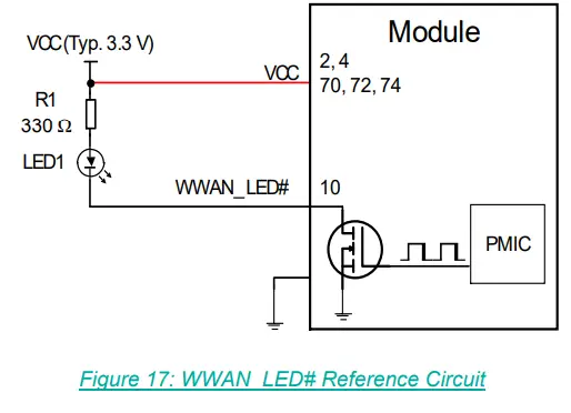
Table 18: Network Status Indications of WWAN_LED#
| WWAN_LED# Logic Level | Description |
| Low (LED On) | RF function is turned on. |
| High (LED Off) | RF function is turned off if any of the following occurs: • The (U)SIM card is not powered. • W_DISABLE1# is at low level (airplane mode enabled). • AT+CFUN=4 and AT+CFUN=0 (RF function disabled). |
4.3.4. WAKE_ON_WAN#
The WAKE_ON_WAN# is an open drain pin, which requires a pull-up resistor on the host. When a URC returns, a one-second low level pulse signal will be outputted to wake up the host.
Table 19: State of the WAKE_ON_WAN#
| WAKE_ON_WAN# State | Module Operation Status |
| Output a one-second pulse signal at low level | SMS/Data is incoming (to wake up the host) |
| Always at high level | Idle/Sleep |

4.3.5. DPR
The module provides a DPR (Dynamic Power Reduction) signal for body SAR (Specific Absorption Rate) detection. The signal is sent by a host system proximity sensor to the module to provide an input trigger which will reduce the output power in the radio transmission.
Table 20: Function of the DPR Signal
| DPR Level | Function |
| High/Floating | Max. transmitting power will not back off |
| Low | Max. transmitting power will back off by executing AT+QCFG=”SAR_DSI” |

NOTE
See document [2] for more details about AT+QCFG=”SAR_DSI”.
4.3.6. WLAN_PA_EN
- In LTE mode, WLAN_PA_EN is set to 0 (low level) by default.
- When WLAN_PA_EN is set to 1 (high level), the LNA will be in self-protection mode.
Table 21: Pin definition of WLAN_PA_EN
| Pin No. | Pin Name | I/O | Description |
| 60 | WLAN_PA_EN | DI | Self-protection of LNA control |
4.4. Cellular/WLAN COEX Interface*
The module provides the cellular/WLAN COEX interface.
The following table shows the pin definition of this interface.
Table 22: Pin Definition of Cellular/WLAN COEX Interface
| Pin No. | Pin Name | I/O | Description |
| 62 | COEX_RXD | DI | LTE/WLAN coexistence receive |
| 64 | COEX_TXD | DO | LTE/WLAN coexistence transmit |
NOTE
Please note that COEX_RXD and COEX_TXD cannot be used as general UART.
4.5. Configuration Pins
Table 23: List of Configuration Pins
| Config_0 (Pin 21) | Config_1 (Pin 69) | Config_2 (Pin 75) | Config_3 (Pin 1) | Module Type and Main Host Interface | Port Configuration |
| GND | GND | NC | NC | WWAN–USB 3.0 | 2 |
Table 24: Pin Definition of Configuration Pins
| Pin No. | Pin Name | I/O | Description |
| 21 | CONFIG_0 | DO | Connected to GND internally |
| 69 | CONFIG_1 | DO | Connected to GND internally |
| 75 | CONFIG_2 | DO | Not connected internally |
| 1 | CONFIG_3 | DO | Not connected internally |
The following figure shows a reference circuit for these four pins.

RF Specifications
Appropriate antenna type and design should be used with matched antenna parameters according to specific application. It is required to perform a comprehensive functional test for the RF design before mass production of terminal products. The entire content of this chapter is provided for illustration only. Analysis, evaluation and determination are still necessary when designing target products.
5.1. Cellular Network
5.1.1. Antenna Interface & Frequency Bands
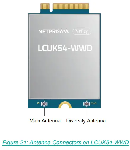
The module provides a main antenna connector and a diversity/GNSS antenna connector, which are used to resist the fall of signals caused by high-speed movement and multipath effect. The impedance of antenna interfaces is 50 Ω.
Table 25: Antenna Connector Definition
| Antenna Connector | I/O | Description | Comment |
| ANT_MAIN | AIO | Main antenna interface:
• LTE: TRX |
|
| RX-Diversity/GNSS antenna interface:
• LTE: DRX |
50 Ω impedance |
||
| ANT_DRX/GNSS | AI |
Table 26: Frequency Bands
| 3GPP Band | Transmit | Receive | Unit |
| WCDMA B1 | 1920–1980 | 2110–2170 | MHz |
| WCDMA B2 | 1850–1910 | 1930–1990 | MHz |
| WCDMA B3 | 1710–1785 | 1805–1880 | MHz |
| WCDMA B4 | 1710–1755 | 2110–2155 | MHz |
| WCDMA B5 | 824–849 | 869–894 | MHz |
| WCDMA B6 | 830–840 | 875–885 | MHz |
| WCDMA B8 | 880–915 | 925–960 | MHz |
| WCDAM B19 | 830–845 | 875–890 | MHz |
| LTE-FDD B1 | 1920–1980 | 2110–2170 | MHz |
| LTE-FDD B2 | 1850–1910 | 1930–1990 | MHz |
| LTE-FDD B3 | 1710–1785 | 1805–1880 | MHz |
| LTE-FDD B4 | 1710–1755 | 2110–2155 | MHz |
| LTE-FDD B5 | 824–849 | 869–894 | MHz |
| LTE-FDD B7 | 2500–2570 | 2620–2690 | MHz |
| LTE-FDD B8 | 880–915 | 925–960 | MHz |
| LTE-FDD B12 | 699–716 | 729–746 | MHz |
| LTE-FDD B13 | 777–787 | 746–756 | MHz |
| LTE-FDD B14 | 788–798 | 758–768 | MHz |
| LTE-FDD B17 | 704–716 | 734–746 | MHz |
| LTE-FDD B18 | 815–830 | 860–875 | MHz |
| LTE-FDD B19 | 830–845 | 875–890 | MHz |
| LTE-FDD B20 | 832–862 | 791–821 | MHz |
| LTE-FDD B25 | 1850–1915 | 1930–1995 | MHz |
| LTE-FDD B26 | 814–849 | 859–894 | MHz |
| LTE-FDD B28 | 703–748 | 758–803 | MHz |
| LTE-FDD B29 7 | – | 717–728 | MHz |
| LTE-FDD B30 | 2305–2315 | 2350–2360 | MHz |
| LTE-FDD B32 7 | – | 1452–1496 | MHz |
| LTE-FDD B66 | 1710–1780 | 2110–2200 | MHz |
| LTE-FDD B71 | 663-698 | 617-652 | MHZ |
| LTE-TDD B34 | 2010-2025 | 2010-2025 | MHZ |
| LTE-TDD B38 | 2570–2620 | 2570–2620 | MHz |
| LTE-TDD B39 | 1880–1920 | 1880–1920 | MHz |
| LTE-TDD B40 | 2300–2400 | 2300–2400 | MHz |
| LTE-TDD B41 | 2496–2690 | 2496–2690 | MHz |
| LTE-TDD B42 | 3400–3600 | 3400–3600 | MHz |
| LTE-TDD B43 | 3600–3800 | 3600–3800 | MHz |
| LTE-TDD B46 7 | – | 5150–5925 | MHz |
7 LTE-FDD B29/B32 and LTE-TDD B46 support Rx only and is only for secondary component carrier.
| LTE-TDD B48 | 3550–3700 | 3550–3700 | MHz |
5.1.2. Antenna Tuner Control Interfaces*
ANTCTL [0:3] and RFFE interfaces are used for antenna tuner control and should be routed to an appropriate antenna control circuit.
5.1.2.1. Antenna Tuner Control Interface through GPIOs
Table 27: Pin Definition of Antenna Tuner Control Interface through GPIOs
| Pin No. | Pin Name | I/O | Description | Comment |
| 59 | ANTCTL0 | DO | 1.8 V | |
| 61 | ANTCTL1 | DO | 1.8 V | |
| Antenna GPIO control | ||||
| 63 | ANTCTL2 | DO | 1.8 V | |
| 65 | ANTCTL3 | DO | 1.8 V |
5.1.2.2. Antenna Tuner Control Interface through RFFE
Table 28: Pin Definition of Antenna Tuner Control Interface through RFFE
| Pin No. | Pin Name | I/O | Description | Comment |
| 56 | RFFE_CLK | DO | Used for external MIPI IC control | 1.8 V |
| 58 | RFFE_DATA | DIO | Used for external MIPI IC control | 1.8 V |
NOTE
If RFFE_CLK and RFFE_DATA are required, please contact NetPrisma for more details.
5.1.3. Tx Power
Table 29: Conducted RF Output Power
| Frequency Band | Modulation | Max. | Min. | Comment |
| WCDMA B1 | BPSK | 23 dBm ±2 dB | < -50 dBm | |
| WCDMA B2 | BPSK | 23 dBm ±2 dB | < -50 dBm | |
| WCDMA B3 | BPSK | 23 dBm ±2 dB | < -50 dBm |
| WCDMA B4 | BPSK | 23 dBm ±2 dB | < -50 dBm | |
| WCDMA B5 | BPSK | 23 dBm ±2 dB | < -50 dBm | |
| WCDMA B6 | BPSK | 23 dBm ±2 dB | < -50 dBm | |
| WCDMA B8 | BPSK | 23 dBm ±2 dB | < -50 dBm | |
| WCDMA B19 | BPSK | 23 dBm ±2 dB | < -50 dBm | |
| LTE-FDD B1 | QPSK | 23.5 dBm ±1 dB | < -40 dBm | 10 MHz, 1RB |
| LTE-FDD B2 | QPSK | 23.5 dBm ±1 dB | < -40 dBm | 10 MHz, 1RB |
| LTE-FDD B3 | QPSK | 23.5 dBm ±1 dB | < -40 dBm | 10 MHz, 1RB |
| LTE-FDD B4 | QPSK | 23.5 dBm ±1 dB | < -40 dBm | 10 MHz, 1RB |
| LTE-FDD B5 | QPSK | 23.5 dBm ±1 dB | < -40 dBm | 10 MHz, 1RB |
| LTE-FDD B7 | QPSK | 23 dBm ±1 dB | < -40 dBm | 10 MHz, 1RB |
| LTE-FDD B8 | QPSK | 23.5 dBm ±1 dB | < -40 dBm | 10 MHz, 1RB |
| LTE-FDD B12 | QPSK | 23.5 dBm ±1 dB | < -40 dBm | 10 MHz, 1RB |
| LTE-FDD B13 | QPSK | 23.5 dBm ±1 dB | < -40 dBm | 10 MHz, 1RB |
| LTE-FDD B14 | QPSK | 23.5 dBm ±1 dB | < -40 dBm | 10 MHz, 1RB |
| LTE-FDD B17 | QPSK | 23.5 dBm ±1 dB | < -40 dBm | 10 MHz, 1RB |
| LTE-FDD B18 | QPSK | 23.5 dBm ±1 dB | < -40 dBm | 10 MHz, 1RB |
| LTE-FDD B19 | QPSK | 23.5 dBm ±1 dB | < -40 dBm | 10 MHz, 1RB |
| LTE-FDD B20 | QPSK | 23.5 dBm ±1 dB | < -40 dBm | 10 MHz, 1RB |
| LTE-FDD B25 | QPSK | 23.5 dBm ±1 dB | < -40 dBm | 10 MHz, 1RB |
| LTE-FDD B26 | QPSK | 23.5 dBm ±1 dB | < -40 dBm | 10 MHz, 1RB |
| LTE-FDD B28 | QPSK | 23.5 dBm ±1 dB | < -40 dBm | 10 MHz, 1RB |
| LTE-FDD B30 | QPSK | 22 dBm ±1 dB | < -40 dBm | 10 MHz, 1RB |
| LTE-FDD B66 | QPSK | 23.5 dBm ±1 dB | < -40 dBm | 10 MHz, 1RB |
| LTE-FDD B71 | QPSK | 23.5 dBm ±1 dB | < -40 dBm | 10 MHz, 1RB |
| LTE-TDD B34 | QPSK | 23.5 dBm ±1 dB | < -40 dBm | 10 MHz, 1RB |
| LTE-TDD B38 | QPSK | 23 dBm ±1 dB | < -40 dBm | 10 MHz, 1RB |
| LTE-TDD B39 | QPSK | 23.5 dBm ±1 dB | < -40 dBm | 10 MHz, 1RB |
| LTE-TDD B40 | QPSK | 23 dBm ±1 dB | < -40 dBm | 10 MHz, 1RB |
| LTE-TDD B41 | QPSK | 23 dBm ±1 dB | < -40 dBm | 10 MHz, 1RB |
| LTE-TDD B42 | QPSK | 21 dBm ±1 dB | < -40 dBm | 10 MHz, 1RB |
| LTE-TDD B43 | QPSK | 21 dBm ±1 dB | < -40 dBm | 10 MHz, 1RB |
| LTE-TDD B48 | QPSK | 21 dBm ±1 dB | < -40 dBm | 10 MHz, 1RB |
5.1.4. Rx Sensitivity
Table 30: Rx Sensitivity
| Frequency Band | SIMO (dBm) 8 | 3GPP (SIMO) (dBm) | Comment 9 |
| WCDMA B1 | -111.5 | -106.7 | |
| WCDMA B2 | -111 | -104.7 | |
| WCDMA B3 | -111 | -103.7 | |
| WCDMA B4 | -111 | -106.7 | |
| WCDMA B5 | -113 | -104.7 | |
| WCDMA B6 | -113 | -106.7 | |
| WCDMA B8 | -113.5 | -103.7 | |
| WCDMA B19 | -113 | -106.7 | |
| LTE-FDD B1 | -100 | -96.3 | 10 MHz |
| LTE-FDD B2 | -100 | -94.3 | 10 MHz |
| LTE-FDD B3 | -100 | -93.3 | 10 MHz |
| LTE-FDD B4 | -99 | -96.3 | 10 MHz |
| LTE-FDD B5 | -101 | -94.3 | 10 MHz |
| LTE-FDD B7 | -98.5 | -94.3 | 10 MHz |
| LTE-FDD B8 | -101 | -93.3 | 10 MHz |
| LTE-FDD B12 | -101 | -93.3 | 10 MHz |
| LTE-FDD B13 | -101 | -93.3 | 10 MHz |
| LTE-FDD B14 | -101 | -93.3 | 10 MHz |
| LTE-FDD B17 | -101 | -93.3 | 10 MHz |
| LTE-FDD B18 | -101 | -96.3 | 10 MHz |
8 SIMO is a smart antenna technology that uses a single antenna at the transmitter side and multiple antennas at the receiver side, which can improve Rx performance.
9 The RB configuration follows 3GPP specification.
| LTE-FDD B19 | -101 | -96.3 | 10 MHz |
| LTE-FDD B20 | -100.5 | -93.3 | 10 MHz |
| LTE-FDD B25 | -99.5 | -92.8 | 10 MHz |
| LTE-FDD B26 | -100.5 | -93.8 | 10 MHz |
| LTE-FDD B28 | -100.5 | -94.8 | 10 MHz |
| LTE-FDD B29 10 | -101 | -93.3 | 10 MHz |
| LTE-FDD B30 | -98 | -95.3 | 10 MHz |
| LTE-FDD B32 10 | -99.5 | -96.3 | 10 MHz |
| LTE-FDD B66 | -99 | -95.8 | 10 MHz |
| LTE-FDD B71 | -100.5 | -94.3 | 10 MHz |
| LTE-TDD B34 | -100 | -96.3 | 10 MHz |
| LTE-TDD B38 | -99.5 | -96.3 | 10 MHz |
| LTE-TDD B39 | -99.5 | -96.3 | 10 MHz |
| LTE-TDD B40 | -98.5 | -96.3 | 10 MHz |
| LTE-TDD B41 | -98.5 | -94.3 | 10 MHz |
| LTE-TDD B42 | -100 | -95.0 | 10 MHz |
| LTE-TDD B43 | -100 | -95.0 | 10 MHz |
| LTE-TDD B46 10 | -95 | -88.5 | 20 MHz |
| LTE-TDD B48 | -99.5 | -95.0 | 10 MHz |
5.2. GNSS 11
5.2.1. Antenna Interface & Frequency Bands
The module includes a fully integrated global navigation satellite system solution.
The module supports standard NMEA 0183 protocol, and outputs NMEA sentences at 1 Hz data update rate via USB interface by default.
By default, the module GNSS engine is switched off. It is to be switched on via AT command. For more details, see document [3].
10 The test results are based on CA_2A-29A, CA_20A-32A and CA_46A-66A. LTE-FDD B29/B32 and LTE-TDD B46 support Rx only and are only for secondary component carrier.
11 GNSS function is optional.
Table 31: GNSS Frequency
| Type | Frequency | Unit |
| GPS/Galileo | 1575.42 ±1.023 | MHz |
| GLONASS | 1601.65 ±4.15 | MHz |
| BDS | 1561.098 ±2.046 | MHz |
| QZSS | 1575.42 ±1.023 | MHz |
5.2.2. GNSS Performance
Table 32: GNSS Performance
| Parameter | Description | Condition | Typ. | Unit |
| Acquisition | Autonomous | -146 | dBm | |
| Sensitivity | Reacquisition | Autonomous | -158 | dBm |
| Tracking | Autonomous | -158 | dBm | |
| Cold start | Autonomous | 35 | s | |
| @ open sky | XTRA start | 13 | s | |
| Warm start | Autonomous | 23 | s | |
| TTFF | @ open sky | XTRA start | 3 | s |
| Hot start | Autonomous | 2 | s | |
| @ open sky | XTRA start | 2 | s |
| Accuracy | CEP-50 | Autonomous @ open sky |
2 | m |
NOTE
- Tracking sensitivity: the minimum GNSS signal power at which the module can maintain lock (keep positioning for at least 3 minutes continuously).
- Reacquisition sensitivity: the minimum GNSS signal power required for the module to maintain lock within 3 minutes after loss of lock.
- Acquisition sensitivity: the minimum GNSS signal power at which the module can fix position successfully within 3 minutes after executing cold start command.
5.3. Antenna Design Requirements
Table 33: Antenna Requirements
| Type | Requirements |
| Main Antenna (WCDMA/LTE Tx/Rx) | • VSWR: ≤ 2 • Efficiency: >30 % • Max Input Power: 50 W • Input Impedance: 50 Ω • Cable Insertion Loss: – < 1 dB: LB (<1 GHz) – < 1.5 dB: MB (1–2.3 GHz) – < 2 dB: LB (> 2.3 GHz) |
| Diversity/GNSS Antenna (WCDMA/LTE/GNSS Rx) |
NOTE
It is recommended to use a passive GNSS antenna when LTE B13 or B14 is supported, as the use of active antenna may generate harmonics which will affect the GNSS performance.
5.4. Antenna Connectors
5.4.1. Antenna Connector Location
The antenna connector locations are shown below.
5.4.2. Antenna Connector Specifications
The module is mounted with standard 2 mm × 2 mm receptacle antenna connectors for convenient antenna connection. The antenna connector’s PN is I-PEX 20449-001E, and the connector dimensions are illustrated as below:

Table 34: Major Specifications of the RF Connectors
| Item | Specification |
| Nominal Frequency Range | DC to 6 GHz |
| Nominal Impedance | 50 Ω |
| Temperature Rating | -40 to +85 °C |
| Voltage Standing Wave Ratio (VSWR) | Meet the requirements of: Max. 1.3 (DC–3 GHz) Max. 1.45 (3–6 GHz) |
5.4.3. Antenna Connector Installation
The receptacle RF connector used in conjunction with the module will accept two types of mated plugs that will meet a maximum height of 1.2 mm using a Ø 0.81 mm coaxial cable or a maximum height of 1.45 mm utilizing a Ø 1.13 mm coaxial cable.
The following figure shows the dimensions of mated plugs using Ø 0.81 mm/Ø1.13 mm coaxial cables:

The following figure illustrates the connection between the receptacle RF connector on the module and the mated plugs using a Ø 0.81 mm coaxial cable.

The following figure illustrates the connection between the receptacle RF connector on the module and the mated plugs using a Ø 1.13 mm coaxial cable.

Figure 25: Space Factor of Mated Connectors (Ø 1.13 mm Coaxial Cables) (Unit: mm)
5.4.4. Recommended RF Connector Installation
5.4.4.1. Assemble Coaxial Cable Plug Manually
The illustration for plugging in a coaxial cable plug is shown below, θ = 90° is acceptable, while θ ≠ 90° is not.

5.4.4.2. Assemble Coaxial Cable Plug with Jig
The pictures of installing the coaxial cable plug with a jig is shown below, θ = 90° is acceptable, while θ ≠ 90° is not.

5.4.5. Recommended Manufacturers of RF Connector and Cable
RF connectors and cables by I-PEX are recommended. For more details, visit https://www.i-pex.com.
Electrical Characteristics and Reliability
6.1. Absolute Maximum Ratings
Absolute maximum ratings for power supply of the module are listed in the following table.
Table 35: Absolute Maximum Ratings
| Parameter | Min. | Typ. | Max. | Unit |
| VCC | -0.3 | 3.3 | 4.7 | V |
6.2. Power Supply Ratings
The typical input voltage of the module is 3.3 V.
Table 36: Power Supply Ratings
| Parameter | Description | Condition | Min. | Typ. | Max. | Unit |
| VCC | Power supply for the module | The actual input voltages must be kept between the minimum and maximum values. | 3.135 | 3.3 | 4.4 | V |
| Voltage Ripple | – | – | – | 30 | 100 | mV |
6.3. Power Consumption
Table 37: Power Consumption (3.7 V Power Supply)
| Parameter | Condition | Typ. | Unit |
| Power-off | Power off | 70 | μA |
| Sleep State | AT+CFUN=0 (USB 2.0 Suspend) | 1.67 | mA |
| AT+CFUN=4 (USB 2.0 Suspend) | 2.28 | mA | |
| WCDMA PF = 64 (USB 2.0 Suspend) | 3.64 | mA | |
| LTE-FDD PF = 64 (USB 2.0 Suspend) | 3.88 | mA | |
| LTE-TDD PF = 64 (USB 2.0 Suspend) | 3.90 | mA | |
| WCDMA PF = 64 | 13.39 | mA | |
| ldle State | LTE-FDD PF = 64 | 13.85 | mA |
| LTE-TDD PF = 64 | 13.61 | mA | |
| WCDMA B1 HSDPA CH10700 @ 22.3 dBm | 748 | mA | |
| WCDMA B1 HSUPA CH10700 @ 22.3 dBm | 660 | mA | |
| WCDMA B2 HSDPA CH9800 @ 22.1 dBm | 640 | mA | |
| WCDMA B2 HSUPA CH9800 @ 22.3dBm | 660 | mA | |
| WCDMA B3 HSDPA CH1338 @ 22.2 dBm | 670 | mA | |
| WCDMA B3 HSUPA CH1338 @ 22.4 dBm | 680 | mA | |
| WCDMA B4 HSDPA CH1638 @22.2 dBm | 670 | mA | |
| WCDMA Data Transmission (GNSS Off) | WCDMA B4 HSUPA CH1638 @ 22.4 dBm | 670 | mA |
| WCDMA B5 HSDPA CH4407 @22.5 dBm | 600 | mA | |
| WCDMA B5 HSUPA CH4407 @ 22.5 dBm | 615 | mA | |
| WCDMA B6 HSDPA CH4400 @ 22.5 dBm | 600 | mA | |
| WCDMA B6 HSUPA CH4400 @ 22.5 dBm | 625 | mA | |
| WCDMA B8 HSDPA CH3012 @22.4 dBm | 650 | mA | |
| WCDMA B8 HSUPA CH3012 @ 22.4 dBm | 650 | mA | |
| WCDMA B19 HSDPA CH738 @ 22.3 dBm | 640 | mA | |
| WCDMA B19 HSUPA CH738 @ 22.6 dBm | 600 | mA | |
| LTE-FDD B1 CH300 @ 23.7 dBm | 840 | mA | |
| LTE-FDD B2 CH900 @ 23.9 dBm | 810 | mA | |
| LTE Data Transmission (GNSS Off) | LTE-FDD B3 CH1575 @ 23.7dBm | 810 | mA |
| LTE-FDD B4 CH2175 @ 23.6 dBm | 830 | mA | |
| LTE-FDD B5 CH2525 @ 23.8 dBm | 760 | mA | |
| LTE-FDD B7 CH3100 @ 23.22 dBm | 950 | mA |
| LTE-FDD B8 CH3625 @ 23.7 dBm | 770 | mA | |
| LTE-FDD B12 CH5095 @ 23.6 dBm | 710 | mA | |
| LTE-FDD B13 CH5230 @ 23.5 dBm | 700 | mA | |
| LTE-FDD B14 CH5330 @ 23.5 dBm | 660 | mA | |
| LTE-FDD B17 CH5790 @ 23.6 dBm | 700 | mA | |
| LTE-FDD B18 CH5925 @ 23.6 dBm | 750 | mA | |
| LTE-FDD B19 CH6075 @ 23.6 dBm | 780 | mA | |
| LTE-FDD B20 CH6300 @ 23.6 dBm | 700 | mA | |
| LTE-FDD B25 CH8365 @ 24 dBm | 820 | mA | |
| LTE-FDD B26 CH8865 @ 23.6 dBm | 840 | mA | |
| LTE-FDD B28 CH9360 @ 23.4 dBm | 710 | mA | |
| LTE-FDD B30 CH9820 @ 22.3 dBm | 1100 | mA | |
| LTE-FDD B66 CH66886 @ 23.6 dBm | 840 | mA | |
| LTE-FDD B71 CH68786 @23.7 dBm | 790 | mA | |
| LTE-TDD B34 CH36275 @ 23.4 dBm | 400 | mA | |
| LTE-TDD B38 CH38000 @ 23.3 dBm | 500 | mA | |
| LTE-TDD B39 CH38450 @ 23.5 dBm | 400 | mA | |
| LTE-TDD B40 CH39150 @ 23.2 dBm | 450 | mA | |
| LTE-TDD B41 CH40740 @ 23.3 dBm | 500 | mA | |
| LTE-TDD B42 CH42590 @ 21.5 dBm | 380 | mA | |
| LTE-TDD B43 CH44590 @ 21.5 dBm | 360 | mA | |
| LTE-TDD B48 CH55990 @ 21.5 dBm | 360 | mA | |
| WCDMA B1 CH10700 @ 23.2 dBm | 780 | mA | |
| WCDMA B2 CH9800 @23.3 dBm | 690 | mA | |
| WCDMA B3 CH1338 @ 23.2 dBm | 720 | mA | |
| WCDMA | WCDMA B4 CH1638 @ 23.2 dBm | 700 | mA |
| WCDMA B5 CH4407 @ 23.2 dBm | 660 | mA | |
| WCDMA B6 CH4400 @23.3 dBm | 650 | mA | |
| WCDMA B8 CH3012 @ 23.4 dBm | 690 | mA |
| WCDMA B19 CH738 @23.3 dBm | 640 | mA |
NOTE
- Power consumption test is carried out under 3.7 V, 25 °C with 5G-M2 EVB, and with thermal dissipation measures.
- For more details about power consumption, please contact NetPrisma Technical Support to obtain the power consumption test report of the modules.
6.4. Digital I/O Characteristics
Table 38: (U)SIM High/Low-voltage I/O Requirements
| Parameter | Description | Min. | Max. | Unit |
| VIH | High-level input voltage | 0.7 × USIM_VDD | USIM_VDD + 0.3 | V |
| VIL | Low-level input voltage | -0.3 | 0.2 × USIM_VDD | V |
| VOH | High-level output voltage | 0.8 × USIM_VDD | – | V |
| VOL | Low-level output voltage | – | 0.4 | V |
Table 39: 1.8 V Digital I/O Requirements
| Parameter | Description | Min. | Max. | Unit |
| VIH | High-level input voltage | 1.65 | 2.1 | V |
| VIL | Low-level input voltage | -0.3 | 0.54 | V |
| VOH | High-level output voltage | 1.3 | – | V |
| VOL | Low-level output voltage | – | 0.4 | V |
Table 40: 3.3 V Digital I/O Requirements
| Parameter | Description | Min. | Max. | Unit |
| 3.3 V | Power Domain | 3.135 | 3.464 | V |
| VIH | High-level input voltage | 2.0 | 3.6 | V |
| VIL | Low-level input voltage | -0.5 | 0.8 | V |
6.5. ESD Protection
Static electricity occurs naturally and it may damage the module. Therefore, applying proper ESD countermeasures and handling methods is imperative. For example, wear anti-static gloves during the development, production, assembly and testing of the module; add ESD protection components to the ESD sensitive interfaces and points in the product design.
Table 41: Electrostatic Discharge Characteristics (Temperature: 25–30 °C, Humidity: 40 ±5 %)
| Tested Interface | Contact Discharge | Air Discharge | Unit |
| VCC, GND | ±5 | ±10 | kV |
| Antenna Interfaces | ±4 | ±8 | kV |
| Other Interfaces | ±0.5 | ±1 | kV |
6.6. Operating and Storage Temperatures
Table 42: Operating and Storage Temperatures
| Parameter | Min. | Typ. | Max. | Unit |
| Operating Temperature Range 12 | -25 | +25 | +75 | ºC |
| Extended Temperature Range 13 | -40 | – | +85 | ºC |
| Storage Temperature Range | -40 | – | +90 | ºC |
12 To meet the normal operating temperature range requirements, it is necessary to ensure effective thermal dissipation, e.g., by adding passive or active heat sinks, heat pipes, vapor chambers. Within the temperature range of -10 °C to +55 °C, the mentioned RF performance margins higher than 3GPP specifications can be guaranteed. When temperature goes beyond temperature range of -10 °C to +55 °C, a few RF performances of module may be slightly off 3GPP specifications. 13 To meet the extended operating temperature range requirements, it is necessary to ensure effective thermal dissipation, e.g., by adding passive or active heat sinks, heat pipes, vapor chambers. Within this range, the module remains the ability to establish and maintain functions such as SMS, without any unrecoverable malfunction. Radio spectrum and radio network are not influenced, while one or more specifications, such as Pout, may undergo a reduction in value, exceeding the specified tolerances of 3GPP. When the temperature returns to the normal operating temperature level, the module will meet 3GPP specifications again.
6.7. Thermal Dissipation

The module offers the best performance when all internal IC chips are working within their operating temperatures. When the IC chip reaches or exceeds the maximum junction temperature, the module may still work but the performance and function (such as RF output power and data rate) will be affected to a certain extent. Therefore, the thermal design should be maximally optimized to ensure all internal IC chips always work within the recommended operating temperature range.
The following principles for thermal consideration are provided for reference:
- Keep the module away from heat sources on your PCB, especially high-power components such as processor, power amplifier, and power supply.
- Maintain the integrity of the PCB copper layer and drill as many thermal vias as possible.
- Expose the copper in the PCB area where module is mounted.
- Apply a soft thermal pad with appropriate thickness and high thermal conductivity between the module and the PCB to conduct heat.
- Follow the principles below when the heatsink is necessary:
– Do not place large size components in the area where the module is mounted on your PCB to reserve enough place for heatsink installation.
– Attach the heatsink to the shielding cover of the module; In general, the base plate area of the heatsink should be larger than the module area to cover the module completely.
– Choose the heatsink with adequate fins to dissipate heat.
– Choose a TIM (Thermal Interface Material) with high thermal conductivity, good softness and good wettability and place it between the heatsink and the module.
– Fasten the heatsink with four screws to ensure that it is in close contact with the module to prevent the heatsink from falling off during the drop, vibration test, or transportation.

Table 43: Maximum Operating Temperature for Main Chips (Unit: °C)
| Baseband Chip | MCP | PMU | WTR | MMPA | PA | APT |
| 85 | 85 | 85 | 85 | 100 | 85 | 85 |
6.8. Notification
Please follow the principles below in the module application.
6.8.1. Coating
If a conformal coating is necessary for the module, do NOT use any coating material that may chemically react with the PCB or shielding cover, and prevent the coating material from flowing into the module.
6.8.2. Cleaning
Avoid using ultrasonic technology for module cleaning since it can damage crystals inside the module.
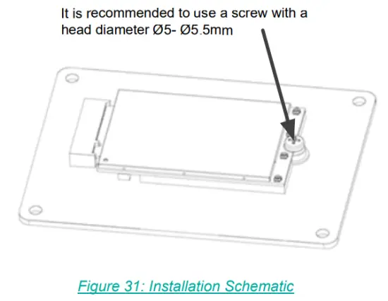
6.8.3. Module Installation
The module needs to be fixed firmly to avoid poor contact caused by shaking. When installing the module, it is recommended to be mounted on the socket with a screw as shown below.
Mechanical Information and Packaging
This chapter mainly describes mechanical dimensions and packaging specifications of LCUK54-WWD.
All dimensions are measured in mm, and the tolerances are ±0.15 mm unless otherwise specified.
7.1. Mechanical Dimensions

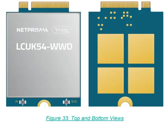
7.2. Top and Bottom Views
NOTE
Images above are for illustration purpose only and may differ from the actual modules. For authentic appearance and label, please refer to the module received from NetPrisma.
7.3. M.2 Connector
The module adopts a standard PCI Express M.2 connector which compiles with the directives and standards listed in PCI Express M.2 Specification.
7.4. Storage Conditions
The storage requirements are shown below.
- Recommended Storage Condition: the temperature should be 23 ±5 °C and the relative humidity should be 35–60 %.
- Shelf life: 12 months in Recommended Storage Condition.
NOTE
Pay attention to ESD protection, such as wearing anti-static gloves, when touching the modules.
7.5. Packaging Specification
This chapter outlines the key packaging parameters and processes. All figures below are for reference purposes only, as the actual appearance and structure of packaging materials may vary in delivery.
The modules are packed in a blister tray packaging as specified in the sub-chapters below.
7.5.1. Blister Tray
Blister tray dimensions are illustrated in the following figure:

7.5.2. Packaging Process
Each blister tray packs 15 modules. Stack 10 trays with modules, and place 1 empty tray on top.
Fasten the 11 trays and place them into a conductive bag and fasten it.

Pack the conductive bag with blister trays into a mini box. 1 mini box can pack 150 modules.
Place the 4 packaged mini boxes into 1 carton and seal it. 1 carton can pack 600 modules.

Figure 35: Packaging Process
Appendix References
Table 44: Related Documents
Document Name
[1] NetPrisma_LCUK54-WWD_CA_Feature
[2] NetPrisma_LCUK54-WWD_AT_Commands_Manual
[3] NetPrisma_LCUK54-WRD_GNSS_Application_Note
[4] NetPrisma_LCUK54-WWD_RF_Application_Note
Table 45: Terms and Abbreviations
| Abbreviation | Description |
| APT | Average Power Tracking |
| AT | Attention |
| BB | Baseband |
| bps | Bit(s) per second |
| BPSK | Binary Phase Shift Keying |
| CA | Carrier Aggregation Certificate Authority |
| CBRS | Citizen Broadband Radio Service |
| COEX | Coexistence |
| DC-HSDPA | Dual-carrier High Speed Downlink Package Access |
| DFOTA | Delta Firmware Upgrade Over-The-Air |
| DL | Downlink |
| DPR | Dynamic Power Reduction |
| DRX | Discontinuous Reception |
| ESD | Electrostatic Discharge |
| eSIM | embedded Subscriber Identity Module |
| ESR | Equivalent Series Resistance |
| FDD | Frequency Division Duplex |
| FTP | File Transfer Protocol |
| HSDPA | High Speed Downlink Packet Access |
| HSPA+ | High Speed Packet Access |
| HSUPA | High Speed Uplink Packet Access |
| HTTP | Hypertext Transfer Protocol |
| HTTPS | Hypertext Transfer Protocol Secure |
| IC | Integrated Circuit |
| kbps | Kilobits per second |
| LAA | License Assisted Access |
| LDO | Low-dropout Regulator |
| LED | Light Emitting Diode |
| LPDDR2 | Low Power Double Data Rate 2 |
| LTE | Long Term Evolution |
| LwM2M | Lightweight M2M |
| MBIM | Mobile Broadband Interface Model |
| Mbps | Megabits per second |
| MCP | Multiple Chip Package |
| ME | Mobile Equipment |
| MFBI | Multi-Frequency Band Indicator |
| MIPI | Mobile Industry Processor Interface |
| MIMO | Multiple-Input Multiple-Output |
| MLCC | Multi-layer Ceramic Capacitor |
| MMPA | Multimode Multiband Power Amplifier |
| MO | Mobile Originated |
| MT | Mobile Terminated |
| NAND | NON-AND |
| NC | Not Connected |
| NITZ | Network Identity and Time Zone / Network Informed Time Zone. |
| NMEA | NMEA (National Marine Electronics Association) 0183 Interface Standard |
| PA | Power Amplifier |
| PC | Personal Computer |
| PCB | Printed Circuit Board |
| PCIe | Peripheral Component Interconnect Express |
| PCM | Pulse Code Modulation |
| PDA | Personal Digital Assistant |
| PDU | Protocol Data Unit |
| PING | Packet Internet Groper |
| PMU | Power Management Unit |
| POS | Point of Sale |
| QAM | Quadrature Amplitude Modulation |
| LNA | Low-Noise Amplifier |
| QMI | Qualcomm MSM (Mobile Station Modems) Interface |
| QPSK | Quadrature Phase Shift Keying |
| RB | Resource Block |
| RF | Radio Frequency |
| RFFE | RF Front-End |
| RoHS | Restriction of Hazardous Substances |
| Rx | Receive |
| SAR | Specific Absorption Rate |
| SDRAM | Synchronous Dynamic Random-Access Memory |
| SIMO | Single Input Multiple Output |
| SMS | Short Message Service |
| TCP | Transmission Control Protocol |
| TDD | Time Division Duplex |
| TRX | Transmit & Receive |
| TVS | Transient Voltage Suppressor |
| Tx | Transmit |
| UART | Universal Asynchronous Receiver/Transmitter |
| UDP | User Datagram Protocol |
| UL | Uplink |
| UMTS | Universal Mobile Telecommunications System |
| URC | Unsolicited Result Code |
| USB | Universal Serial Bus |
| (U)SIM | (Universal) Subscriber Identity Module |
| VIH | High-level Input Voltage |
| VIHmax | Maximum High-level Input Voltage |
| VIHmin | Minimum High-level Input Voltage |
| VIL | Low-level Input Voltage |
| VILmax | Maximum Low-level Input Voltage |
| Vmax | Maximum Voltage |
| Vmin | Minimum Voltage |
| Vnom | Nominal Voltage |
| VOH | High-level Output Voltage |
| VOL | Low-level Output Voltage |
| WCDMA | Wideband Code Division Multiple Access |
| WTR | Wafer-scale RF transceiver |
| WWAN | Wireless Wide Area Network |
9.1 FCC
9.1.1. Important Notice to OEM integrators
- This module is limited to OEM installation ONLY.
- This module is limited to installation in mobile or fixed applications, according to Part 2.1091(b).
- The separate approval is required for all other operating configurations, including portable configurations with respect to Part 2.1093 and different antenna configurations.
- For FCC Part 15.31 (h) and (k): The host manufacturer is responsible for additional testing to verify compliance as a composite system. When testing the host device for compliance with Part 15 Subpart B, the host manufacturer is required to show compliance with Part 15 Subpart B while the transmitter module(s) are installed and operating. The modules should be transmitting and the evaluation should confirm that the module’s intentional emissions are compliant (i.e. fundamental and out of band
emissions). The host manufacturer must verify that there are no additional unintentional emissions other than what is permitted in Part 15 Subpart B or emissions are complaint with the transmitter(s) rule(s).
The Grantee will provide guidance to the host manufacturer for Part 15 B requirements if needed.
9.1.2. Important Note
notice that any deviation(s) from the defined parameters of the antenna trace, as described by the instructions, require that the host product manufacturer must notify to XXXX that they wish to change the antenna trace design. In this case, a Class II permissive change application is required to be filed by the USI, or the host manufacturer can take responsibility through the change in FCC ID (new application) procedure followed by a Class II permissive change application.
9.1.3. End Product Labeling
When the module is installed in the host device, the FCC/IC ID label must be visible through a window on the final device or it must be visible when an access panel, door or cover is easily re-moved. If not, a second label must be placed on the outside of the final device that contains the following text: “Contains FCC ID: 2BEY3LCUK54WWDA” “Contains IC: 32052-LCUK54WWDA “ The FCC ID/IC ID can be used only when all FCC/IC compliance requirements are met.
9.1.4. Antenna Installation
- The antenna must be installed such that 20 cm is maintained between the antenna and users,
- The transmitter module may not be co-located with any other transmitter or antenna.
- Only antennas of the same type and with equal or less gains as shown below may be used with this module. Other types of antennas and/or higher gain antennas may require additional authorization for operation.
| Band | MAX Gain (dBi) |
| WCDMA B2 | 8.00 |
| WCDMA B4 | 5.00 |
| WCDMA B5 | 9.42 |
| LTE B2 | 8.50 |
| LTE B4 | 5.50 |
| LTE B5 | 9.91 |
| LTE B7 | 9.00 |
| LTE B12 | 9.20 |
| LTE B13 | 9.66 |
| LTE B14 | 9.73 |
| LTE B17 | 9.24 |
| LTE B25 | 8.50 |
| LTE B26(814-824) | 9.86 |
| LTE B26(824-849) | 9.91 |
| LTE B30 | 0.98 |
| LTE B38 | 9.00 |
| LTE B41 | 9.00 |
| LTE B42 | 8.00 |
| LTE B43 | 1.00 |
| LTE B48 | 1.00 |
| LTE B66 | 5.50 |
| LTE B71 | 8.98 |
In the event that these conditions cannot be met (for example certain laptop configurations or colocation with another transmitter), then the FCC/IC authorization is no longer considered valid and the FCC ID/IC ID cannot be used on the final product. In these circumstances, the OEM integrator will be responsible for re-evaluating the end product (including the transmitter) and obtaining a separate FCC/IC authorization.
9.1.5. Manual Information to the End User
The OEM integrator has to be aware not to provide information to the end user regarding how to install or remove this RF module in the user’s manual of the end product which integrates this module. The end user manual shall include all required regulatory information/warning as show in this manual.
9.1.6. Federal Communication Commission Interference Statement
This device complies with Part 15 of the FCC Rules. Operation is subject to the following two conditions:
(1) This device may not cause harmful interference, and (2) this device must accept any interference received, including interference that may cause undesired operation.
This equipment has been tested and found to comply with the limits for a Class B digital device, pursuant to Part 15 of the FCC Rules. These limits are designed to provide reasonable protection against harmful interference in a residential installation. This equipment generates, uses and can radiate radio frequency energy and, if not installed and used in accordance with the instructions, may cause harmful interference to radio communications. However, there is no guarantee that interference will not occur in a particular installation. If this equipment does cause harmful interference to radio or television reception, which can be determined by turning the equipment off and on, the user is encouraged to try to correct the interference by one of the following measures:
– Reorient or relocate the receiving antenna.
– Increase the separation between the equipment and receiver.
– Connect the equipment into an outlet on a circuit different from that to which the receiver is connected.
– Consult the dealer or an experienced radio/TV technician for help.
Any changes or modifications not expressly approved by the party responsible for compliance could void the user’s authority to operate this equipment. This transmitter must not be co-located or operating in conjunction with any other antenna or transmitter.
9.1.7. List of applicable FCC rules
This module has been tested and found to comply with part 22, part 24, part 27 and part 90 requirements for Modular Approval.
The modular transmitter is only FCC authorized for the specific rule parts (i.e., FCC transmitter rules) listed on the grant, and that the host product manufacturer is responsible for compliance to any other FCC rules that apply to the host not covered by the modular transmitter grant of certification. If the grantee markets their product as being Part 15 Subpart B compliant (when it also contains unintentional-radiator digital circuity), then the grantee shall provide a notice stating that the final host product still requires Part 15 Subpart B compliance testing with the modular transmitter installed.
9.1.8. This device is intended only for OEM integrators under the following conditions:(For module device use)
- The antenna must be installed such that 20 cm is maintained between the antenna and users, and
- The transmitter module may not be co-located with any other transmitter or antenna.
As long as 2 conditions above are met, further transmitter test will not be required. However, the OEM integrator is still responsible for testing their end-product for any additional compliance requirements required with this module installed.
9.1.9. Radiation Exposure Statement
This equipment complies with FCC radiation exposure limits set forth for an uncontrolled environment.
This equipment should be installed and operated with minimum distance 20 cm between the radiator & your body.
9.2. IC
9.2.1. Industry Canada Statement
This device complies with Industry Canada’s licence-exempt RSSs. Operation is subject to the following two conditions:
(1) This device may not cause interference; and
(2) This device must accept any interference, including interference that may cause undesired operation of the device
9.2.2. Radiation Exposure Statement
This equipment complies with IC radiation exposure limits set forth for an uncontrolled environment. This equipment should be installed and operated with minimum distance 20 cm between the radiator & your body.
9.2.4. This device is intended only for OEM integrators under the following conditions: (For module device use)
1) The antenna must be installed such that 20 cm is maintained between the antenna and users, and
2) The transmitter module may not be co-located with any other transmitter or antenna.
As long as 2 conditions above are met, further transmitter test will not be required. However, the OEM integrator is still responsible for testing their end-product for any additional compliance requirements required with this module installed.
9.2.6. IMPORTANT NOTE:
In the event that these conditions can not be met (for example certain laptop configurations or colocation with another transmitter), then the Canada authorization is no longer considered valid and the IC ID can not be used on the final product. In these circumstances, the OEM integrator will be responsible for re-evaluating the end product (including the transmitter) and obtaining a separate Canada authorization.
9.2.8. End Product Labeling
This transmitter module is authorized only for use in device where the antenna may be installed such that 20 cm may be maintained between the antenna and users. The final end product must be labeled in a visible area with the following: “Contains IC: 32052-LCUK54WWDA”.
9.2.10.Manual Information To the End User
The OEM integrator has to be aware not to provide information to the end user regarding how to install or remove this RF module in the user’s manual of the end product which integrates this module.
The end user manual shall include all required regulatory information/warning as show in this manual.
9.2.12 Antenna Requirements
The following antennae were approved with the prototype:
This radio transmitter [32052-LCUK54WWDA] has been approved by innovation, Science and development Economic Canada to operate with the types of antennas listed below, with the maximum allowable gain indicated. The types of antennas not included in this list that have a gain of any type lis ted are strictly prohibited for use with this device.
| Band | Description | MAX Gain (dBi) |
| WCDMA B2 |
PIFA Antenna |
3.87 |
| WCDMA B4 | 3.91 | |
| WCDMA B5 | 3.32 | |
| LTE B2 | 3.87 | |
| LTE B4 | 3.91 | |
| LTE B5 | 3.32 | |
| LTE B7 | 3.16 | |
| LTE B12 | 3.19 | |
| LTE B13 | 3.28 | |
| LTE B14 | 3.25 | |
| LTE B17 | 3.19 | |
| LTE B25 | 3.87 | |
| LTE B26(824-849) | 3.32 | |
| LTE B30 | 0.98 | |
| LTE B38 | 3.07 | |
| LTE B41 | 3.16 | |
| LTE B42 | 2.35 | |
| LTE B43 | 1.94 | |
| LTE B48 | 1.00 | |
| LTE B66 | 3.91 | |
| LTE B71 | 3.07 |
LCUK54-WWD_Hardware_Design
![]()
Documents / Resources
 |
NETPRISMA LCUK54-WWD Module [pdf] User Manual 2BEY3LCUK54WWDA, lcuk54wwda, LCUK54-WWD Module, LCUK54-WWD, Module |