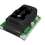
neptronic CMMB102 Dual Mini I and O Communication Module

Specifications:
- Model: CMMB102
- Input Voltage: 24 Vac or 24 Vdc
- Consumption: 3VA (175mA @ 24 Vac)
- Universal Inputs: 4 [0.00-10.00Vdc, 10K/20K/30K, on/off (dry contact), 4.00-20.00mA]
- Universal Outputs: 2 [0-10Vdc, pulsed signal (20mA drive), on/off]
- Binary Relay Outputs: OptoFET (250mA max)
- BACnet/Modbus Communication
- Operational Temperature: TBD
- Storage Temperature: TBD
- Relative Humidity: TBD
- Weight: TBD
- Dimensions:
- A = 3.18 / 81 mm
- B = 4.93 / 125 mm
- C = 2.27 / 58 mm
Product Usage Instructions
Connections and Configurations:
All jumper settings must be set to the same value through
BACnet. Some configurations are only available through BACnet.
Network Settings:
- Network Mode Options:
- If BACnet:
- Auto Detect*
- Manual (see DS2-1 & DS2-2)
- If Modbus:
- Config via Modbus Register
- If BACnet:
- Baud Rate:
- OFF OFF: 9,600
- ON OFF: 19,200
- OFF ON: 38,400
- ON ON: BACnet – 76,800, Modbus – 57,600
- MAC Address: The 8 DIP switches represent a binary logic to calculate the MAC address.
- End of Line: None* / 120 ohms (*default setting)
Network Port and Universal Inputs:
Network Port (TB6): A+, B-, BCOM
Universal Inputs (TB7-8): Selectable Inputs AI1 to AI4 with respective COM connections.
Analog and Binary Outputs:
AO1-AO2 Selector (JP1-JP2) for Binary Output or Analog Output selection.
Voltage Input (TB1): 24V, max 175mA.Universal Outputs (TB2-3): Selectable Outputs AO1/BO1 and AO2/BO2 with respective COM connections.
Binary Outputs (TB4-5): BO3 and BO4 with respective COM connections.
AI1-AI4 Signal (JP4-JP7): I = 4-20mA, T = Thermistor / on-off, V = 0-10Vdc.
AO1-AO2 Switches (SW1-SW2): On = 10Vdc, Auto* = Automatic, Off = 0Vdc.
BO1-BO2 Switches (SW1-SW2): On = Activated, Auto* = Automatic, Off = Deactivated.
BO3-BO4 Switches (SW3-SW4): On = Activated, Auto* = Automatic, Off = Deactivated.
FAQ
- Q: How do I set the network mode for the CMMB102?
- A: For BACnet mode, ensure the setting is on Auto Detect or manually configure through DS2-1 & DS2-2. For Modbus mode, set it to Config via Modbus Register.
- Q: What is the default MAC address configuration for the CMMB102?
- A: The default MAC address is calculated when all DIP switches are set to OFF for BACnet and all OFF for Modbus.
- Q: How do I select the analog or binary output for the CMMB102?
- A: Use the AO1-AO2 Selector (JP1-JP2) to choose between binary output or analog output.
Description
The CMMB extends your BACnet or Modbus network when your application requires additional inputs and outputs on a physical controller. Combining the 8 inputs and outputs of the CMMB with your Building Automation System provides simple expansion of a new or existing controller and reduces unnecessary costs of additional components.
Features
Power & Communication
- 24Vac or 24Vdc supply
- BACnet® MS/TP or Modbus communication port (selectable)
Inputs & Outputs
- 4 universal inputs
- 2 universal outputs (supervised)
- 2 binary outputs (supervised)
Installation
- 4 override switches to manually control each output
- LED status indication of each input and output
- DIN rail mounting
- Removable, non-strip, raising clamp terminals
- removable see-through panel for easy access to DIP switches
Network Communication
- BACnet® MS/TP or Modbus communication port (selectable via DIP switch)
- Select the MAC address via the DIP switch or via the network
BACnet®
- MS/TP @ 9600, 19200, 38400 or 76800 bps
- Automatic baud rate detection
- Automatic device instance configuration
- Copy & broadcast configuration to other CMMB modules
Modbus
- Modbus @ 9600, 19200, 38400 or 57600 bps
- RTU Slave, 8 bits (configurable parity and stop bits)
- Connects to any Modbus master
Technical Specifications
| Specifications | CMMB102 |
| Input Voltage | 24 Vac or 24 Vdc |
| Consumption | 3VA (175mA @ 24 Vac) |
| Universal Inputs | 4 [0.00-10.00Vdc, 10KΩ/20KΩ/30KΩ, on/off (dry contact), 4.00-20.00mA] / 12b hardware resolution with oversampling |
| Universal Outputs | 2 [0-10Vdc, pulsed signal (20mA drive), on/off] / 1mV resolution OptoFET (250mA max) |
| Binary Relay Outputs | 2 [normally open/closed, independent common per relay, 5A resistive] |
| BACnet | BACnet® MS/TP @ 9600, 19200, 38400 or 76800 bps (BAS-C) |
| Modbus | Modbus RTU slave @ 9600, 19200, 38400 or 57600. Selectable parity and stop bit configuration:
· No parity, 2 stop bit · Even parity, 1 stop bit · Odd parity, 1 stop bit |
| Communication Connections | 24 AWG twisted-shield cable (Belden 9841 or equivalent) |
| Electrical Connections | 0.8 mm2 [18 AWG] minimum |
| Operational Temperature | 0ºC to 50ºC [32ºF to 122ºF] |
| Storage Temperature | -30ºC to 50ºC [-22ºF to 122ºF] |
| Relative Humidity | 5 a 95% non condensed |
| Weight | 0.2 kg [0.4 lb] |
| Dimensions
A = 3.18” / 81 mm B = 4.93” / 125 mm C = 2.27” / 58 mm |

|
Connections and Configurations
Please note that all jumper settings must also be set to the same value through BACnet. Some additional configurations are only available through BACnet (see Network Conditions

MAC Address DIP Switch (DS1)
MAC addresses for BACnet and Modbus communication, are selectable by DIP switch DS1 using binary logic.
BACnet
- The highest MAC address is 254.
- Default is all switches OFF = MAC address 0
- If you do not change the device instance in program mode, it will be automatically modified according to the MAC address.
| MAC Address | DS.1 = 1 | DS.2 = 2 | DS.3 = 4 | DS.4 = 8 | DS.5 = 16 | DS.6 = 32 | DS.7 = 64 | DS.8 = 128 | Default Device Instance |
| 0 | OFF | OFF | OFF | OFF | OFF | OFF | OFF | OFF | 153000 |
| 1 | ON | OFF | OFF | OFF | OFF | OFF | OFF | OFF | 153001 |
| 2 | OFF | ON | OFF | OFF | OFF | OFF | OFF | OFF | 153002 |
| 3 | ON | ON | OFF | OFF | OFF | OFF | OFF | OFF | 153003 |
| 4 | OFF | OFF | ON | OFF | OFF | OFF | OFF | OFF | 153004 |
| … | … | … | … | … | … | … | … | … | … |
| 126 | OFF | ON | ON | ON | ON | ON | ON | OFF | 153126 |
| … | … | … | … | … | … | … | … | … | … |
| 254 | OFF | ON | ON | ON | ON | ON | ON | ON | 153254 |
Modbus
- The highest MAC address is 247.
- Default is all switches OFF = MAC address 1
- MAC address is binary value +1
- There is no device instance for Modbus.
| MAC Address | DS.1 = 1 | DS.2 = 2 | DS.3 = 4 | DS.4 = 8 | DS.5 = 16 | DS.6 = 32 | DS.7 = 64 | DS.8 = 128 |
| 0+1 = 1 | OFF | OFF | OFF | OFF | OFF | OFF | OFF | OFF |
| 1+1 = 2 | ON | OFF | OFF | OFF | OFF | OFF | OFF | OFF |
| 2+1 = 3 | OFF | ON | OFF | OFF | OFF | OFF | OFF | OFF |
| 3+1 = 4 | ON | ON | OFF | OFF | OFF | OFF | OFF | OFF |
| 4+1 = 5 | OFF | OFF | ON | OFF | OFF | OFF | OFF | OFF |
| … | … | … | … | … | … | … | … | … |
| 126+1 = 127 | OFF | ON | ON | ON | ON | ON | ON | OFF |
| … | … | … | … | … | … | … | … | … |
| 246+1 = 247 | OFF | ON | ON | OFF | ON | ON | ON | ON |
LEDs
Power
On = Input voltage normal
Off = No power
Status
Flashing = Normal operation (watchdog)
RX/TX (BACnet)
Flashing = Receiving (RX) and/or transmitting (TX) data.
RX/TX (Modbus)
Flashing = Receiving (RX) and/or transmitting (TX) data.
Input Status
On = Input on
Off = Input off
Flashing = Input not connected (thermistor setting only)
Analog = When Universal Inputs are set to analog values (Vdc, mA, or Thermistor); the LED intensity corresponds to the input value. For example: At 10Vdc, the LED will be fully on. At 5Vdc, the LED will be at 50% intensity. At 0 Vdc, the LED will be off.
Output Status
On = Activated
Off = Deactivated
Flashing = Output pulsed
Analog = When Universal and Analog outputs are set to analog values (Vdc); the LED intensity corresponds to the output value. For example: At 10Vdc, the LED will be fully on. At 5Vdc, the LED will be at 50% intensity. At 0 Vdc, the LED will be off.
Network Conditions
Please note that all jumper settings must also be set to the same value through BACnet or Modbus. The following is a list of conditions and additional BACnet or Modbus objects.
Universal Inputs (AI1-AI4)
- For temperature thermistor reading: with the jumper set to Thermistor, set the AI input type to 10K_TypeG, 10K_Type3A1, 10K_Type4A1, 10K_NTC, 20K_Type6A1 or 30K_Type6A1.
- For on/off contact input reading: with the hardware jumper set to Thermistor, set the AI input type to Digital_Input. The polarity can also be set to direct or reverse. For example, in Reverse an “on” signal would be recognized as an “off” signal.
- For analog 0-10 Vdc input reading: with the hardware jumper set to 0-10 Vdc, set the AI input type to 0_10V.
Universal/Analog Outputs (AO1-AO2)
- You can set the polarity to direct or reverse. For example, in reverse the output range would be 10-0 Vdc instead of 0-10 Vdc. The polarity applies to all settings 0-10Vdc, on/off and pulsed.
- You can also set the outputs to pulsed or digital on/off.
- A fixed output value can only be modified via BACnet when the override switch is in the “Automatic” position.
Binary Outputs (BO1-BO4)
- A fixed output (open/closed) can only be modified via BACnet when the override switch is in the “Automatic” position.
- The displayed text can be set to either Open/Closed, On/Off, or Alarm/Normal (BACnet only).
Supervised Outputs
- All outputs are fully supervised via BACnet. This provides the actual state of the output including any manual overrides done using the on-board switches.
Pulse Counting Feature
The pulse counting feature enables counting the number of pulses detected by the inputs.
- When an active edge is detected, the Pulse Count is incremented by 1 up to the Prescaler value. When the Prescaler value is reached, the Accumulator is incremented by 1 and the Pulse Count is reset to 0.
- A value that is higher than 80% of the input’s saturation confirms a high level. A value that is lower than 20% of the input’s saturation confirms a low level.
- The maximum frequency is 100Hz and the minimum pulse length is 5ms/50%D.C.

Output Configuration
Output LEDs LD1 and LD2 will always respond to the output mode selected on MSV.54/55 and the analog value set on AV.72/73 irrespective of the position of JP1 and JP2. The position of JP1 and JP2 determines the output objects to be used as shown below:
| JP1 and JP2 Position | Output Objects to be used | ||
| JP1 in Analog Position | AV.52, AV.54, AV.72, AV.506, BV.66, MSV.54, MSV.110 | ||
| JP2 in Analog Position | AV.53, AV.55, AV.73, AV.507, BV.67, MSV.55, MSV.111 | ||
|
JP1 in Binary Position |
Common | MSV.100 = TPM | MSV.100 = On/Off |
| MSV.100 | AV.500 | BV.22 | |
| MSV.106 | MSV.66 | ||
|
JP2 in Binary Position |
Common | MSV.100 = TPM | MSV.100 = On/Off |
| MSV.101 | AV.501 | BV.23 | |
| MSV.107 | MSV.67 | ||
Note: Refer to the BACnet Objects Table on page 5 for the description of the BACnet objects listed.
BACnet Objects Table
|
ID1 |
Name |
Description |
Writable? |
Notes (* = default)
(† = only when UniversalInputxFunction is set to 10K_Type3/G) |
|
AI.1 |
UniversalInput1 |
Universal input 1 mode selected by MSV.1. |
Out of service |
0 to 10Volt or -40 to 100ºC (150ºC)† or
-40 to 212ºF (302ºF)† or 4 to 20mA or 0 to 1 Resolution: 0.01Volt or 0.01ºC/0.02ºF or 0.01mA or 1 |
|
AI.2 |
UniversalInput2 |
Universal input 2 mode selected by MSV.12. |
Out of service |
0 to 10Volt or -40 to 100ºC (150ºC)† or
-40 to 212ºF (302ºF)† or 4 to 20mA or 0 to 1 Resolution: 0.01Volt or 0.01ºC/0.02ºF or 0.01mA or 1 |
|
AI.3 |
UniversalInput3 |
Universal input 3 mode selected by MSV.15. |
Out of service |
0 to 10Volt or -40 to 100ºC (150ºC)† or
-40 to 212ºF (302ºF)† or 4 to 20mA or 0 to 1 Resolution: 0.01Volt or 0.01ºC/0.02ºF or 0.01mA or 1 |
|
AI.4 |
UniversalInput4 |
Universal input 4 mode selected by MSV.48. |
Out of service |
0 to 10Volt or -40 to 100ºC (150ºC)† or
-40 to 212ºF (302ºF)† or 4 to 20mA or 0 to 1 Resolution: 0.01Volt or 0.01ºC/0.02ºF or 0.01mA or 1 |
| AV.1 | UI1PulseCount | Universal input 1 pulse count. | Present Value | 0 to 16777216, Resolution: 1 |
| AV.2 | UI2PulseCount | Universal input 2 pulse count. | Present Value | 0 to 16777216, Resolution: 1 |
| AV.3 | UI3PulseCount | Universal input 3 pulse count. | Present Value | 0 to 16777216, Resolution: 1 |
| AV.4 | UI4PulseCount | Universal input 4 pulse count. | Present Value | 0 to 16777216, Resolution: 1 |
| AV.11 | UI1Accumulator | Universal input 1 pulse counter rollovers. | Present Value | 0 to 16777216, Resolution: 1 |
| AV.12 | UI2Accumulator | Universal input 2 pulse counter rollovers. | Present Value | 0 to 16777216, Resolution: 1 |
| AV.13 | UI3Accumulator | Universal input 3 pulse counter rollovers. | Present Value | 0 to 16777216, Resolution: 1 |
| AV.14 | UI4Accumulator | Universal input 4 pulse counter rollovers. | Present Value | 0 to 16777216, Resolution: 1 |
| AV.52 | AnalogOutput1Min | Min. voltage of analog output 1. | Present Value | 0* Volt to AV.54 | Resolution 0.1 Volt |
| AV.53 | AnalogOutput2Min | Min. voltage of analog output 2. | Present Value | 0* Volt to AV.55 | Resolution 0.1 Volt |
| AV.54 | AnalogOutput1Max | Max. voltage of analog output 1. | Present Value | AV.52 to 10.0* Volt | Resolution 0.1 Volt |
| AV.55 | AnalogOutput2Max | Max. voltage of analog output 2. | Present Value | AV.53 to 10.0* Volt | Resolution 0.1 Volt |
| AV.72 | AnalogOutput1 | Analog output 1 value. | Present Value | 0-100% | Resolution 0.1% |
| AV.73 | AnalogOutput2 | Analog output 2 value. | Present Value | 0-100% | Resolution 0.1% |
| AV.226 | UniversalInput1Offset | Universal input 1 offset. | Present Value | -5.00 to 5.00 ºC/ºF/Volt/mA (default 0*)
Resolution: 0.1 ºC/ºF/Volt/mA |
| AV.227 | UniversalInput2Offset | Universal input 2 offset. | Present Value | -5.00 to 5.00 ºC/ºF/Volt/mA (default 0*)
Resolution: 0.1 ºC/ºF/Volt/mA |
| AV.228 | UniversalInput3Offset | Universal input 3 offset. | Present Value | -5.00 to 5.00 ºC/ºF/Volt/mA (default 0*)
Resolution: 0.1 ºC/ºF/Volt/mA |
| AV.229 | UniversalInput4Offset | Universal input 4 offset. | Present Value | -5.00 to 5.00 ºC/ºF/Volt/mA (default 0*)
Resolution: 0.1 ºC/ºF/Volt/mA |
| AV.468 | CopyCfgStartAdd | Copy configuration start address. | Present Value | 0-254 Address of first CMMB to copy Available only if BV.101 is set to No |
|
AV.469 |
CopyCfgEndAdd |
Copy configuration end address. |
Present Value |
AV.468 – (AV.468 + 64)
Address of last CMMB to copy Available only if BV.101 is set to No |
|
AV.470 |
CopyCfgResult2 |
Copy configuration result. |
Present Value |
AV.468 – AV.469
The result of copy is available on the Description property and is available only if BV.101 is set to Yes. Results: Succeed, Prog_Error, Type_Error, Model_Error, FW_Error, Mem_Error, Size_Error, Comm_Error, SlaveDevice, InProgress, AllSucceed |
| AV.500 | TPMOutput1 | TPM Output 1 value. | Present Value | 0-100% | Resolution 0.1% |
| AV.501 | TPMOutput2 | TPM Output 2 value. | Present Value | 0-100% | Resolution 0.1% |
| AV.506 | AO1FailsafePreset | Analog output 1 failsafe preset value. | Present Value | 0 to 100%, Resolution: 0.1% |
- ID is equal to ObjectType.Instance
- Write the address in the present value, result will be available in the description.
|
ID1 |
Name |
Description |
Writable? |
Notes (* = default)
(† = only when UniversalInputxFunction is set to 10K_Type3/G) |
|
| AV.507 | AO2FailsafePreset | Analog output 2 failsafe preset value. | Present Value | 0 to 100%, Resolution: 0.1% | |
| AV.508 | TimeoutValue | Network Timeout value. | Present Value | 5 to 600 sec, Resolution: 5 sec | |
| AV.509 | UI1PulsePrescaler | Universal input 1 pulse counter rollover threshold. | Present Value | 0 to 16777216, Resolution: 1 | |
| AV.510 | UI2PulsePrescaler | Universal input 2 pulse counter rollover threshold. | Present Value | 0 to 16777216, Resolution: 1 | |
| AV.511 | UI3PulsePrescaler | Universal input 3 pulse counter rollover threshold. | Present Value | 0 to 16777216, Resolution: 1 | |
| AV.512 | UI4PulsePrescaler | Universal input 4 pulse counter rollover threshold. | Present Value | 0 to 16777216, Resolution: 1 | |
|
BV.22 |
ContactOutput1 |
Binary output 1 status. |
Present Value |
0= Open / Ouvert / Off / Arret / Normal * 1= Close / Fermé / On / Marche / Alarm Text depends of selection in MSV.66 | |
|
BV.23 |
ContactOutput2 |
Binary output 2 status. |
Present Value |
0= Open / Ouvert / Off / Arret / Normal * 1= Close / Fermé / On / Marche / Alarm Text depends of selection in MSV.67 | |
|
BV.24 |
ContactOutput3 |
Binary output 3 status. |
Present Value |
0= Open / Ouvert / Off / Arret / Normal * 1= Close / Fermé / On / Marche / Alarm Text depends of selection in MSV.68 | |
|
BV.25 |
ContactOutput4 |
Binary output 4 status. |
Present Value |
0= Open / Ouvert / Off / Arret / Normal * 1= Close / Fermé / On / Marche / Alarm Text depends of selection in MSV.69 | |
| BV.66 | AnalogOutput1Direction | Polarity of analog output 1. | Present Value | 0= Direct *
1= Reverse |
|
| BV.67 | AnalogOutput2Direction | Polarity of analog output 2. | Present Value | 0= Direct *
1= Reverse |
|
| BV.93 | UI1_DI_Polarity | Polarity of universal input 1 when used in digital input mode. | Present Value | 0= Direct *
1= Reverse |
|
| BV.94 | UI2_DI_Polarity | Polarity of universal input 2 when used in digital input mode. | Present Value | 0= Direct *
1= Reverse |
|
| BV.95 | UI3_DI_Polarity | Polarity of universal input 3 when used in digital input mode. | Present Value | 0= Direct *
1= Reverse |
|
| BV.96 | UI4_DI_Polarity | Polarity of universal input 4 when used in digital input mode. | Present Value | 0= Direct *
1= Reverse |
|
|
BV.101 |
CopyCfgExecute |
Start or stop copy configuration. |
Present Value |
0= No *
1= Yes Start copy and give results, must be reset by user. CopyCfgExecute does not apply to the failsafe settings on the outputs. |
|
| BV.102 | SystemUnit | Select the unit system to use on the device. | Present Value | 0= Celsius *
1= Fahrenheit |
|
| BV.103 | Inhibit Output Override | Inhibit the override of the outputs. | Present Value | 0= Off *
1= On |
|
| BV.104 | TimeoutStatus | Network timeout status. | Present Value | 0= Inactive *
1= Active |
|
|
MSV.1 |
UniversalInput1Function |
Selected analog input 1 mode. |
Present Value |
1= 0_10V
2= 4_20mA 3= 10K_Type3/G * 4= 10K_Type3A1 5= 10K_Type4A1 |
6= 10K_Type2
7= 20K_Type6A1 8= 30K_Type6A1 9= Digital_Input 10= 10K_NTC_Carel |
|
MSV.12 |
UniversalInput2Function |
Selected analog input 2 mode. |
Present Value |
1= 0_10V
2= 4_20mA 3= 10K_Type3/G * 4= 10K_Type3A1 5= 10K_Type4A1 |
6= 10K_Type2
7= 20K_Type6A1 8= 30K_Type6A1 9= Digital_Input 10= 10K_NTC_Carel |
|
MSV.15 |
UniversalInput3Function |
Selected analog input 3 mode. |
Present Value |
1= 0_10V
2= 4_20mA 3= 10K_Type3/G * 4= 10K_Type3A1 5= 10K_Type4A1 |
6= 10K_Type2
7= 20K_Type6A1 8= 30K_Type6A1 9= Digital_Input 10= 10K_NTC_Carel |
|
MSV.48 |
UniversalInput4Function |
Selected analog input 4 mode. |
Present Value |
1= 0_10V
2= 4_20mA 3= 10K_Type3/G * 4= 10K_Type3A1 5= 10K_Type4A1 |
6= 10K_Type2
7= 20K_Type6A1 8= 30K_Type6A1 9= Digital_Input 10= 10K_NTC_Carel |
|
ID1 |
Name |
Description |
Writable? |
Notes (* = default)
(† = only when UniversalInputxFunction is set to 10K_Type3/G) |
|
MSV.54 |
AnalogOutput1Mode |
Select analog output 1 mode. |
Present Value |
1= Analog *
2= On_Off 3= Pulsing |
|
MSV.55 |
AnalogOutput2Mode |
Select analog output 2 mode. |
Present Value |
1= Analog *
2= On_Off 3= Pulsing |
|
MSV.66 |
ContactOutput1Text |
Contact output 1 inactive & active text. |
Present Value |
1= Open_Close *
2= Ouvert_Fermé 3= On_Off 4= Marche_Arret 5= Alarm_Normal |
|
MSV.67 |
ContactOutput2Text |
Contact output 2 inactive & active text. |
Present Value |
1= Open_Close *
2= Ouvert_Fermé 3= On_Off 4= Marche_Arret 5= Alarm_Normal |
|
MSV.68 |
ContactOutput3Text |
Contact output 3 inactive & active text. |
Present Value |
1= Open_Close *
2= Ouvert_Fermé 3= On_Off 4= Marche_Arret 5= Alarm_Normal |
|
MSV.69 |
ContactOutput4Text |
Contact output 4 inactive & active text. |
Present Value |
1= Open_Close *
2= Ouvert_Fermé 3= On_Off 4= Marche_Arret 5= Alarm_Normal |
| MSV.100 | OptofetOutput1Mode | Select Optofet output 1 mode. | Present Value | 1= On_Off *
2= TimePulseModulation |
| MSV.101 | OptofetOutput2Mode | Select Optofet output 2 mode. | Present Value | 1= On_Off *
2= TimePulseModulation |
|
MSV.106 |
CfgBO1FailsafeMode |
Configuration of the binary output 1 failsafe mode. |
Present Value |
1= LastState *
2= Open 3= Close |
|
MSV.107 |
CfgBO2FailsafeMode |
Configuration of the binary output 2 failsafe mode. |
Present Value |
1= LastState *
2= Open 3= Close |
|
MSV.108 |
CfgBO3FailsafeMode |
Configuration of the binary output 3 failsafe mode. |
Present Value |
1= LastState *
2= Open 3= Close |
|
MSV.109 |
CfgBO4FailsafeMode |
Configuration of the binary output 4 failsafe mode. |
Present Value |
1= LastState *
2= Open 3= Close |
| MSV.110 | CfgAO1FailsafeMode | Configuration of the analog output 1 failsafe mode. | Present Value | 1= LastState *
2= Preset |
| MSV.111 | CfgAO2FailsafeMode | Configuration of the analog output 2 failsafe mode. | Present Value | 1= LastState *
2= Preset |
Modbus Registers
- Register address
- As per the protocol base (base 0); for PLC add 1 to the protocol base.
- As per holding register (base 40001)
- Functions :
- 03 Read Holding Register
- 06 Write Single Register
- 16 Write Multiple Registers
- Error Codes :
- 02 Illegal Data Address
- 03 Illegal Value
- 06 Slave Device Busy
- W = Writable register, [blank] = read-only.
- No Real number in Modbus register, use scale to calculate real number. Register = Real number * Scale => Real number = Register / Scale. Scale could be 1, 10 or 100
- Attention when writing a register that contains a bit string. If bit is writable (conditional or not), the write will always be accepted. If bit is reserved or not writable, the write will be ignored and will keep its actual state.
- Use the READ-MODIFY-WRITE sequence.
|
Protocol Base |
Holding Register |
Description |
Data Type |
MSB/LSB |
Units/Values |
Writable |
Default Value | |||
| MB | LB | |||||||||
| 0 | 40001 | MSB = Neptronic Device ID LSB = MAC Address | Unsigned | 105 (69h) | [1..247]
(1h- F7h) |
* MAC address is writable if all DIP switches of DS2 are OFF. | W* | 69h | 1h | |
|
1 |
40002 |
Device Baud Rate |
Unsigned Scale 0.01 |
[96] [192] [384] [576] | 9,600
19,200 38,400 57,600 |
96 |
||||
|
2 |
40003 |
COM Port Configuration
IMPORTANT: The default value is “no parity, 2 stop bits”. To change the value, you must set DIP switch DS1-3 to OFF. If set to ON, it will always remain at the default value. Refer to Connections and Configurations on page 2. |
Unsigned |
[0..2] |
0 = no parity, 2 stop bits 1 = even parity, 1 stop bit 2 = odd parity, 1 stop bit |
W |
0 |
|||
| 3 | 40004 | Product Name (characters 8 & 7) | 2 x ASCII | char 8 | char 7 | Valid ASCII character: 32 (20h) – 122 (7ah), Empty = 0 | W | 43h [C] | 40h [M] | |
| 4 | 40005 | Product Name (characters 6 & 5) | 2 x ASCII | char 6 | char 5 | Valid ASCII character: 32 (20h) – 122 (7ah), Empty = 0 | W | 40h [M] | 42h [B] | |
| 5 | 40006 | Product Name (characters 4 & 3) | 2 x ASCII | char 4 | char 3 | Valid ASCII character: 32 (20h) – 122 (7ah), Empty = 0 | W | 31h [1] | 30h [0] | |
| 6 | 40007 | Product Name (characters 2 & 1) | 2 x ASCII | char 2 | char 1 | Valid ASCII character: 32 (20h) – 122 (7ah), Empty = 0 | W | 36h [6] | 20h [ ] | |
| 7 | 40008 | Firmware Version | Unsigned Scale 100 | 103 | 1.03 | 103 | ||||
| 8 | 40009 | Application Version | Unsigned Scale 100 | 100 | 1.00 | 100 | ||||
|
Protocol Base |
Holding Register |
Description |
Data Type |
MSB/LSB |
Units/Values |
Writable |
Default Value | ||
| MB | LB | ||||||||
|
9 |
40010 |
System Status 1 |
Bit String |
[B0..B15] |
0 = Normal
1 = Fault – – – – – – – – – – – – – – – – – – – B0 = System operation |
0000, 0001, 1111, 1110b |
|||
| 10 | 40011 | System Status 2 | Bit String | [B0..B15] | Always 0 | 0000, 0000, 0000, 0000b | |||
|
11 |
40012 |
Analog Input 1 |
0-10V: Type: Unsigned, Scale:100, Unit: Volt, Range: 0.00-10.00V, Resolution: 0.01 4-20mA: Type: Unsigned, Scale:100, Unit: mA, Range: 4.00-20.00 mA, Resolution: 0.01 10K Type 3A1, 10K Type 4AI, 10K Type 2, 20K Type 6AI, 30K Type 6AI:
Type: Signed, Scale:100, Unit: ºC, Range: -40.00 – 100.00 ºC, Resolution: 0.01 Type: Signed, Scale:100, Unit: ºF, Range: -40.00 – 212.00 ºF, Resolution: 0.02 10K Type 3/G: Type: Signed, Scale:100, Unit: ºC, Range: -40.00 – 150.00 ºC, Resolution: 0.01 Type: Signed, Scale:100, Unit: ºF, Range: -40.00 – 302.00 ºF, Resolution: 0.02 DI: Type: Unsigned, Scale:1, No Unit, Range: 0-1, Resolution: 1 |
0 |
|||||
|
12 |
40013 |
Analog Input 2 |
0 |
||||||
|
13 |
40014 |
Analog Input 3 |
0 |
||||||
|
14 |
40015 |
Analog Input 4 |
0 |
||||||
| 15 to 19 | 40016 to
40020 |
Reserved | |||||||
| 20 | 40021 | Analog Output 1 | Unsigned Scale 10 | [0..1000] |
Unit: %, Range: 0-100.0%, Resolution: 0.1 |
W |
0 | ||
| 21 | 40022 | Analog Output 2 | 0 | ||||||
| 22 to 23 | 40023 to
40024 |
Reserved | 0 | ||||||
|
24 |
40025 |
Relay Output |
Bit String |
[B0..B5] | B0 = Relay 1
B1 = Relay 2 B2 = Relay 3 |
B3 = Relay 4
B4 to B5 = Reserved |
W |
0000, 0000, 0000, 0000b |
|
|
25 |
40026 |
Output Overwrite Status
Indicates that the output is overridden by the hardware switch (SW1-SW4). |
Bit String |
[B0..B9] | B0 = Relay 1 B1 = Relay 2 B2 = Relay 3
B3 = Relay 4 |
B4 = AO1 B5 = AO2
B6 to B9 = Reserved |
0000, 0000, 0000, 0000b |
||
| 26 | 40027 | Universal Input 1 Function |
Unsigned |
[1..10] |
1= 0_10V
2= 4_20mA 3= 10K_Type3/G * 4= 10K_Type3A1 5= 10K_Type4A1 |
6= 10K_Type2
7= 20K_Type6A1 8= 30K_Type6A1 9= Digital_Input 10= 10K_NTC_Carel |
W |
3 | |
| 27 | 40028 | Universal Input 2 Function | 3 | ||||||
| 28 | 40029 | Universal Input 3 Function | 3 | ||||||
| 29 | 40030 | Universal Input 4 Function | 3 | ||||||
| 30 to 33 | 40031 to
40034 |
Reserved | |||||||
|
Protocol Base |
Holding Register |
Description |
Data Type |
MSB/LSB |
Units/Values |
Writable |
Default Value | |||
| MB | LB | |||||||||
| 34 | 40035 | Universal Input 1 Offset |
Signed Scale 100 |
[0..100] |
Range: +/- 5.00, Resolution: 0.1 |
W |
0 | |||
| 35 | 40036 | Universal Input 2 Offset | 0 | |||||||
| 36 | 40037 | Universal Input 3 Offset | 0 | |||||||
| 37 | 40038 | Universal Input 4 Offset | 0 | |||||||
| 38 to 41 | 40039 to
40042 |
Reserved | ||||||||
|
42 |
40043 |
Analog Output 1 Mode |
Unsigned |
[1..3] | 1 = Analog
2 = On/Off 3 = Pulse |
W |
1 |
|||
| 43 | 40044 | Analog Output 1 Minimum Voltage | Signed Scale 10 | [0..100] | Unit: Volt, | Range: 0 V – Register 44, Resolution: 0.1 |
W |
0 | ||
| 44 | 40045 | Analog Output 1 Maximum Voltage | Unit: Volt, Range: Register 43 – 10.0V, Resolution: 0.1 | 100 | ||||||
|
45 |
40046 |
Analog Output 2 Mode |
Unsigned |
[1..3] | 1 = Analog
2 = On/Off 3 = Pulse |
W |
1 |
|||
| 46 | 40047 | Analog Output 2 Minimum Voltage | Signed Scale 10 | [0..100] | Unit: Volt, | Range: 0 V – Register 47, Resolution: 0.1 |
W |
0 | ||
| 47 | 40048 | Analog Output 2 Maximum Voltage | Unit: Volt, | Range: Register 46 – 10.0V, Resolution: 0.1 | 100 | |||||
| 48 to 53 | 40049 to
40054 |
Reserved | ||||||||
| 0 = Direct | 0 = Off | |||||||||
| 1 = Reverse | 1 = On | |||||||||
| – – – – – – – – – – – – – – – – – – – | – – – – – – – – – – – – – – – – – – – | |||||||||
| B0 = AO1 polarity | B14 = Inhibit Output Override | |||||||||
| System Options | B1 = AO2 polarity | – – – – – – – – – – – – – – – – – – – | ||||||||
| 54 | 40055 | Bit String | [B0..B15] | B2 to B3 = Reserved | 0 = Celsius | W | 0000, 0000, 0000, 0000b | |||
| * = digital input mode only | B4 = AI1 polarity * | 1 = Fahrenheit | ||||||||
| B5 = AI2 polarity * | – – – – – – – – – – – – – – – – – – – | |||||||||
| B6 = AI3 polarity * | B15 = System Unit | |||||||||
| B7 = AI4 polarity * | ||||||||||
| B8 to B13 = Reserved | ||||||||||
| 55 | 40056 | TPM Output 1 | Unsigned Scale 10 | [0..1000] |
Unit: %, |
Range: 0-100.0%, Resolution: 0.1 |
W |
0 | ||
| 56 | 40057 | TPM Output 2 | 0 | |||||||
| 57 to 60 | 40058 to
40061 |
Reserved | ||||||||
| 61 | 40062 | Optofet Output 1 Mode |
Bit String |
[1, 2] | 1 = On_Off
2 = TimePulseModulation |
W |
1 | |||
| 62 | 40063 | Optofet Output 2 Mode | 1 | |||||||
|
Protocol Base |
Holding Register |
Description |
Data Type |
MSB/LSB |
Units/Values |
Writable |
Default Value | |
| MB | LB | |||||||
| 63 to 66 | 40064 to
40067 |
Reserved | ||||||
|
67 |
40068 |
Binary Output 1 Fail Safe Mode |
Unsigned |
[1..3] | 1= LastState
2= Open 3= Close |
W |
1 |
|
|
68 |
40069 |
Binary Output 2 Fail Safe Mode |
Unsigned |
[1..3] | 1= LastState
2= Open 3= Close |
W |
1 |
|
|
69 |
40070 |
Binary Output 3 Fail Safe Mode |
Unsigned |
[1..3] | 1= LastState
2= Open 3= Close |
W |
1 |
|
|
70 |
40071 |
Binary Output 4 Fail Safe Mode |
Unsigned |
[1..3] | 1= LastState
2= Open 3= Close |
W |
1 |
|
| 71 | 40072 | Analog Output 1 Fail Safe Mode | Unsigned | [1,2] | 1= LastState
2= Preset |
W | 1 | |
| 72 | 40073 | Analog Output 1 Fail Safe Preset Value | Unsigned Scale 10 | [0..1000] | Unit: %, Range: 0 – 100.00 %, Resolution: 0.1 | W | 100 | |
| 73 | 40074 | Analog Output 2 Fail Safe Mode | Unsigned | [1,2] | 1= LastState
2= Preset |
W | 1 | |
| 74 | 40075 | Analog Output 2 Fail Safe Preset Value | Unsigned Scale 10 | [0..1000] | Unit: %, Range: 0 – 100.00 %, Resolution: 0.1 | W | 100 | |
| 75 | 40076 | Timeout Status | Unsigned | [0,1] | 0= Inactive
1= Active |
0 | ||
| 76 | 40077 | Network Timeout Value | Unsigned Scale 1 | [5..600] | Unit: Seconds (sec), Range: 5 – 600 sec, Resolution: 5 sec | W | 30 | |
| 77 | 40078 | UI1 Pulse Prescaler (0) | Unsigned Scale 1 | [0…16777216] | Range: 0 to 16777216, Resolution: 1 | W | 1 | |
| 78 | 40079 | UI1 Pulse Prescaler (1) | [0…16777216] | Range: 0 to 16777216, Resolution: 1 | ||||
| 79 | 40080 | UI2 Pulse Prescaler (0) | Unsigned Scale 1 | [0…16777216] | Range: 0 to 16777216, Resolution: 1 | W | 1 | |
| 80 | 40081 | UI2 Pulse Prescaler (1) | [0…16777216] | Range: 0 to 16777216, Resolution: 1 | ||||
| 81 | 40082 | UI3 Pulse Prescaler (0) | Unsigned Scale 1 | [0…16777216] | Range: 0 to 16777216, Resolution: 1 | W | 1 | |
| 82 | 40083 | UI3 Pulse Prescaler (1) | [0…16777216] | Range: 0 to 16777216, Resolution: 1 | ||||
| 83 | 40084 | UI4 Pulse Prescaler (0) | Unsigned Scale 1 | [0…16777216] | Range: 0 to 16777216, Resolution: 1 | W | 1 | |
| 84 | 40085 | UI4 Pulse Prescaler (1) | [0…16777216] | Range: 0 to 16777216, Resolution: 1 | ||||
| 85 to 92 | 40086 to
40093 |
Reserved | ||||||
|
Protocol Base |
Holding Register |
Description |
Data Type |
MSB/LSB |
Units/Values |
Writable |
Default Value | |
| MB | LB | |||||||
| 93 | 40094 | UI1 Pulse Count (0) | Unsigned Scale 1 | [0…16777216] | Range: 0 to 16777216, Resolution: 1 | W | 0 | |
| 94 | 40095 | UI1 Pulse Count (1) | [0…16777216] | Range: 0 to 16777216, Resolution: 1 | ||||
| 95 | 40096 | UI2 Pulse Count (0) | Unsigned Scale 1 | [0…16777216] | Range: 0 to 16777216, Resolution: 1 | W | 0 | |
| 96 | 40097 | UI2 Pulse Count (1) | [0…16777216] | Range: 0 to 16777216, Resolution: 1 | ||||
| 97 | 40098 | UI3 Pulse Count (0) | Unsigned Scale 1 | [0…16777216] | Range: 0 to 16777216, Resolution: 1 | W | 0 | |
| 98 | 40099 | UI3 Pulse Count (1) | [0…16777216] | Range: 0 to 16777216, Resolution: 1 | ||||
| 99 | 40100 | UI4 Pulse Count (0) | Unsigned Scale 1 | [0…16777216] | Range: 0 to 16777216, Resolution: 1 | W | 0 | |
| 100 | 40101 | UI4 Pulse Count (1) | [0…16777216] | Range: 0 to 16777216, Resolution: 1 | ||||
| 101 to
108 |
40102 to
40109 |
Reserved | ||||||
| 109 | 40110 | UI1 Accumulator (0) | Unsigned Scale 1 | [0…16777216] | Range: 0 to 16777216, Resolution: 1 | W | 0 | |
| 110 | 40111 | UI1 Accumulator (1) | [0…16777216] | Range: 0 to 16777216, Resolution: 1 | ||||
| 111 | 40112 | UI2 Accumulator (0) | Unsigned Scale 1 | [0…16777216] | Range: 0 to 16777216, Resolution: 1 | W | 0 | |
| 112 | 40113 | UI2 Accumulator (1) | [0…16777216] | Range: 0 to 16777216, Resolution: 1 | ||||
| 113 | 40114 | UI3 Accumulator (0) | Unsigned Scale 1 | [0…16777216] | Range: 0 to 16777216, Resolution: 1 | W | 0 | |
| 114 | 40115 | UI3 Accumulator (1) | [0…16777216] | Range: 0 to 16777216, Resolution: 1 | ||||
| 115 | 40116 | UI4 Accumulator (0) | Unsigned Scale 1 | [0…16777216] | Range: 0 to 16777216, Resolution: 1 | W | 0 | |
| 116 | 40117 | UI4 Accumulator (1) | [0…16777216] | Range: 0 to 16777216, Resolution: 1 | ||||
| 117 to
124 |
40118 to
40125 |
Reserved | ||||||
 Recycling at end of life: please return this product to your Neptronic local distributor for recycling. If you need to find the nearest Neptronic authorized distributor, please consult www.neptronic.com.
Documents / Resources
 |
neptronic CMMB102 Dual Mini I and O Communication Module [pdf] Instruction Manual CMMB102 Dual Mini I and O Communication Module, CMMB102, Dual Mini I and O Communication Module, I and O Communication Module, Communication Module, Module |