LINEAR TECHNOLOGY LTM8042 LED Driver Module Instructions
DESCRIPTION
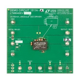
Demonstration circuits 1511A-A and 1511A-B feature the LTM®8042 and the LTM8042-1, which are respectively com- plete 1A and 350mA µModule LED drivers. The demonstra- tion circuits are assembled as boost topologies, accepting an input voltage from 3V to 30V and supporting an output up to 32V (see Table 1). The default switching frequency is 600kHz for DC1511A-A and 950kHz for DC1511A-B, but can be adjusted by changing the value of RT. mode and buck mode (step-down). DC1511A includes a
DC1511A is easily configured to support other features, including PWM dimming, analog dimming, buck-boost P-channel MOSFET that is necessary for PWM dimming. The RADJ pin/terminal voltage controls the output current. Voltage is either applied directly to the terminal or set by a divider that includes resistor RADJ and the LTM8042’s internal 2V reference and divider resistor. Open LED over- voltage protection is also included. Consult the LTM8042/ LTM8042-1 datasheet for further information on how to properly use or modify the circuit.
Design files for this circuit board are available at http://www.linear.com/demo
L, LT, LTC, LTM, µModule, Linear Technology and the Linear logo are registered trademarks of Linear Technology Corporation. All other trademarks are the property of their respective owners.
PERFORMANCE SUMMARY Specifications are at TA = 25°C
| PARAMETER | CONDITIONS/NOTES | VALUE |
| Input Voltage Range, VIN (BSTIN) | 3V to 30V (See Table 1) | |
| ILED | DC1511A-A (LTM8042) DC1511A-B (LTM8042-1)
Current Derating May Be Necessary Under Certain VIN, VOUT , Frequency and Thermal Conditions |
1A
350mA |
| Switching Frequency | RT = 30.1k (DC1511A-A) RT = 16.9k (DC1511A-B) | 600kHz 950kHz |
| Maximum Output Voltage (Open LED Voltage) | 36V | |
| Efficiency | VIN = 12V, VLED = 16.7V, ILED = 1A
VIN = 12V, VLED = 24.8V, ILED = 350mA |
91.5% (See Figure 2)
89% (See Figure 3) |
BOARD PHOTO
QUICK START PROCEDURE
Demonstration circuit 1511A is easy to set up to evaluate the performance of the LTM8042EV/LTM8042EV-1. Refer to Figure 1 for the proper measurement equipment set- up and follow the procedure below for a boost (step-up) topology.
- Connect a string of LEDs with forward voltage 32V or less, but greater than the input voltage, to the LED+ (LED anode) and GND (LED cathode) terminals on the PCB, as shown in Figure 1.
- With the power off, connect the input power supply to the BSTIN/BKLED– and GND terminals within the ranges specified in Table 1. Preset the DC input voltage within the recommended input voltage range for the appropriate forward voltage of the LED string.
Table 1. Input Range for Proper Operation (Refer to the
LTM8042/LTM8042-1 Datasheet)
| DC1511A-A LTM8042 | DC1511A-B LTM8042-1 | ||
| INPUT VOLTAGE (BSTIN/BKLED– TO GND) | LED STRING VOLTAGE (LED+ TO GND) | INPUT VOLTAGE (BSTIN/BKLED– TO GND) | LED STRING VOLTAGE (LED+ TO GND) |
| 5V to 5.8V | 6V to 9V | 3.2V to 7V | 8V to 12V |
| 6.4V to 7.7V | 8V to 12V | 4.1V to 10V | 12V to 16V |
| 8.6V to 11.3V | 12V to 16V | 4.8V to 12.3V | 15V to 21V |
| 11.3V to 13.8V | 15V to 21V | 5.8V to 15V | 18V to 24V |
| 13.4V to 16.5V | 18V to 24V | 8.5V to 20.8V | 24V to 32V |
| 20.5V to 22.5V | 24V to 32V | ||
3. Connect the PWM terminal. If PWM is not used, connect PWM to a 5V source or to the input voltage. PWM must be pulled high or the LEDs will remain off.
4. Turn the input power supply on.
5. Observe the LED string running at the programmed LED current.
6. For PWM dimming, connect a PWM 100Hz or higher frequency signal to the PWM terminal.
7. Observe the reduction of brightness in the LED string by varying the duty cycle of the PWM signal.
To use the DC1511A in a buck-boost mode topology, make the following modifications to the procedure.
- At step 1, connect the cathode of the LED string to the BSTIN/BKLED– The LED forward voltage may be greater than the input voltage for buck-boost mode.
- At step 2, refer to the datasheet buck-boost mode applications information table. Preset the DC input voltage within the recommended input voltage range for the appropriate forward voltage and current of the LED
To use the DC1511A in a buck mode (step-down) topology, make the following modifications to the procedure.
- Remove the 0Ω jumper at location R8 and instead install the jumper at location This shorts the VCC, TGEN and RUN pins/terminals to BSTOUT/BKIN instead of BSTIN/BKLED–.
- At step 1, connect the cathode of the LED string to the BSTIN/BKLED– The LED forward voltage must be less than the input voltage for buck mode.
At step 2, connect the input power supply to BSTOUT/ BKIN and GND. Refer to the datasheet buck mode applications information table. Preset the DC input voltage within the recommended input voltage range for the appropriate forward voltage and current of the LED string.
QUICK START PROCEDURE

Figure 1. Proper Measurement Equipment Set-Up (Boost Topology)

Figure 2. DC1511A-A Efficiency vs VIN Boost Operation, 16.7V at 1A LED String

Figure 3. DC1511A-B Efficiency vs VIN Boost Operation, 24.8V at 350mA LED String
DEMO MANUAL DC1511A
PARTS LIST
LTM8042EV
| ITEM | QTY | REFERENCE | PART DESCRIPTION | MANUFACTURER/PART NUMBER |
Required Circuit Components
| 1 | 1 | C1 | Cap., X5R, 4.7µF, 50V, 20%, 1206 | Taiyo Yuden UMK316BJ475ML-T |
| 2 | 1 | C2 | Cap., X5R, 10µF, 50V, 20%, 1210 | Taiyo Yuden UMK325BJ106MM-T |
| 3 | 1 | C4 | Cap., X7R, 0.01µF, 25V, 10%, 0603 | AVX 06033C103KAT2A |
| 4 | 1 | RT | Res., Chip, 30.1k, 0.06W, 1%, 0603 | NIC NRC06F3012TRF |
| 5 | 1 | U1 | I.C., LED Driver, LGA (77),15mm × 9mm × 4.32mm | Linear Technology Corporation LTM8042EV |
Additional Demo Board Circuit Components
| 1 | 1 | C3 | Cap., X5R, 1µF, 50V, 20%, 1206 | TDK C3216X5R1H105M |
| 2 | 0 | C5 (OPT) | Cap., 1206 | |
| 3 | 0 | RADJ, R2, R3, R5, R7 (OPT) | Res., 0603 | |
| 4 | 1 | RSYNC | Res., Chip, 100k, 0.06W, 5%, 0603 | NIC NRC06J104TRF |
| 5 | 2 | R1, R6 | Res./Jumper, Chip, 0Ω, 1/16W, 1A, 0603 | Vishay CRCW06030000Z0EA |
| 6 | 0 | R4 (OPT) | Res., 1206 | |
| 7 | 1 | R8 | Res./Jumper, Chip, 0Ω, 1/4W, 1A, 1206 | Vishay CRCW12060000ZOEA |
| 8 | 1 | M1 | P-Channel MOSFET, 40V, SOT-23 | Vishay Si2319DS-T1-E3 #PBF |
Hardware, for Demo Board Only
| 1 | 13 | E1, E2, E3, E4, E5, E6, E7, E8, E9, E10, E11, E12, E13 | Turret, Testpoint 0.094″ | Mill-Max 2501-2-00-80-00-00-07-0 |
LTM8042EV-1
| ITEM | QTY | REFERENCE | PART DESCRIPTION | MANUFACTURER/PART NUMBER |
Required Circuit Components
| 1 | 1 | C1 | Cap., X5R, 2.2µF, 50V, 20%, 1206 | Taiyo Yuden UMK316BJ225MD-T |
| 2 | 1 | C2 | Cap., X5R, 10µF, 50V, 20%, 1210 | Taiyo Yuden UMK325BJ106MM-T |
| 3 | 1 | C4 | Cap., X7R, 0.01µF, 25V, 10%, 0603 | AVX 06033C103KAT2A |
| 4 | 1 | RT | Res., Chip, 16.9k, 0.06W, 1%, 0603 | Vishay CRCW060316K9FKEA |
| 5 | 1 | U1 | I.C., LED Driver, LGA (77),15mm × 9mm × 4.32mm | Linear Technology Corporation LTM8042EV-1 |
Additional Demo Board Circuit Components
| 1 | 1 | C3 | Cap., X5R, 1µF, 50V, 20%, 1206 | TDK C3216X5R1H105M |
| 2 | 0 | C5 (OPT) | Cap., 1206 | |
| 3 | 0 | RADJ, R2, R3, R5, R7 (OPT) | Res., 0603 | |
| 4 | 1 | RSYNC | Res., Chip, 100k, 0.06W, 5%, 0603 | NIC NRC06J104TRF |
| 5 | 2 | R1, R6 | Res./Jumper, Chip, 0Ω, 1/16W, 1A, 0603 | Vishay CRCW06030000Z0EA |
| 6 | 0 | R4 (OPT) | Res., 1206 | |
| 7 | 0 | R8 | Res./Jumper, Chip, 0Ω, 1/4W, 1A, 1206 | Vishay CRCW12060000ZOEA |
| 8 | 1 | M1 | P-Channel MOSFET, 40V, SOT-23 | Vishay Si2319DS-T1-E3 #PBF |
Hardware, for Demo Board Only
| 1 | 13 | E1, E2, E3, E4, E5, E6, E7, E8, E9, E10, E11, E12, E13 | Turret, Testpoint, 0.094″ | Mill-Max 2501-2-00-80-00-00-07-0 |
SCHEMATIC DIAGRAM

Information furnished by Linear Technology Corporation is believed to be accurate and reliable. However, no responsibility is assumed for its use. Linear Technology Corporation makes no representation that the interconnection of its circuits as described herein will not infringe on existing patent rights.
DEMONSTRATION BOARD IMPORTANT NOTICE
Linear Technology Corporation (LTC) provides the enclosed product(s) under the following AS IS conditions:
This demonstration board (DEMO BOARD) kit being sold or provided by Linear Technology is intended for use for ENGINEERING DEVELOPMENT OR EVALUATION PURPOSES ONLY and is not provided by LTC for commercial use. As such, the DEMO BOARD herein may not be complete in terms of required design-, marketing-, and/or manufacturing-related protective considerations, including but not limited to product safety measures typically found in finished commercial goods. As a prototype, this product does not fall within the scope of the European Union direc- tive on electromagnetic compatibility and therefore may or may not meet the technical requirements of the directive, or other regulations.
If this evaluation kit does not meet the specifications recited in the DEMO BOARD manual the kit may be returned within 30 days from the date of delivery for a full refund. THE FOREGOING WARRANTY IS THE EXCLUSIVE WARRANTY MADE BY THE SELLER TO BUYER AND IS IN LIEU OF ALL OTHER WARRANTIES, EXPRESSED, IMPLIED, OR STATUTORY, INCLUDING ANY WARRANTY OF MERCHANTABILITY OR FITNESS FOR ANY PARTICULAR PURPOSE. EXCEPT TO THE EXTENT OF THIS INDEMNITY, NEITHER PARTY SHALL BE LIABLE TO THE OTHER FOR ANY INDIRECT, SPECIAL, INCIDENTAL, OR CONSEQUENTIAL DAMAGES.
The user assumes all responsibility and liability for proper and safe handling of the goods. Further, the user releases LTC from all claims arising from the handling or use of the goods. Due to the open construction of the product, it is the user’s responsibility to take any and all appropriate precautions with regard to electrostatic discharge. Also be aware that the products herein may not be regulatory compliant or agency certified (FCC, UL, CE, etc.).
No License is granted under any patent right or other intellectual property whatsoever. LTC assumes no liability for applications assistance, customer product design, software performance, or infringement of patents or any other intellectual property rights of any kind.
LTC currently services a variety of customers for products around the world, and therefore this transaction is not exclusive.
Please read the DEMO BOARD manual prior to handling the product. Persons handling this product must have electronics training and observe good laboratory practice standards. Common sense is encouraged.
This notice contains important safety information about temperatures and voltages. For further safety concerns, please contact a LTC applica- tion engineer.
Mailing Address:
Linear Technology 1630 McCarthy Blvd.
Milpitas, CA 95035
Copyright © 2004, Linear Technology Corporation
Read More About This Manual & Download PDF:
Documents / Resources
 |
LINEAR TECHNOLOGY LTM8042 LED Driver Module [pdf] Instructions LTM8042, LTM8042-1, LTM8042 LED Driver Module, LTM8042, LED Driver Module |


