![]()
DEMO MANUAL DC2088A
High Density LTC3880
Step-Down DC/DC Converter with
Power System Management
DESCRIPTION
Demonstration circuit 2088A is a high current, high density, two-phase single output synchronous buck converter featuring the LTC3880EUJ, a dual-phase current mode controller. The LT C ® 3880 has the PMBus interface and power system management functions.
The layout of DC2088A is very compact and the total solution is within a 1.0″ × 1.0″ area. The DrMOS is used on the board for high current, high efficiency. The input range of this board is from 7V to 14V, and the output voltage can be programmed from 0.8V to 1.8V, with an output current up to 50A. The factory default setting for the output is 1.0V. The DC2088A also has an on-board dynamic load circuit, which makes it easy for the customer to evaluate the transient performances.
The DC2088A powers up to default settings and produces power based on configuration resistors or NVM without the need for any serial bus communication. This allows easy evaluation of the DC/DC converter aspects of the LTC3880. To fully explore the extensive power system management features of the parts, download the GUI software LTpowerPlay onto your PC and use LT C ’s I2 C/ SMBus/PMBus Dongle DC1613A to connect to the board. LTpowerPlay allows the user to reconfigure the part on the fly and store the configuration in EEPROM, view telemetry of voltage, current, temperature and fault status.
GUI DOWNLOAD
The software can be downloaded from:
www.linear.com/ltpowerplay
For more details and instructions on LTpowerPlay, please refer to “LTpowerPlay for LTC3880 Quick Start Guide”.
Design files for this circuit board are available at
http://www.linear.com/demo
 , LT, LTC, LTM, Linear Technology and the Linear logo are registered trademarks of Linear Technology Corporation. All other trademarks are the property of their respective owners.
PERFORMANCE SUMMARY
Specifications are at TA = 25°C
| SYMBOL | PARAMETER | CONDITIONS | MIN | TYP | MAX | UNITS |
| VIN | Input Supply Range | 7 | 12 | 14 | V | |
| VOUT | Output Voltage Range | IOUT = 0A TO 50A, VIN = 7.0V to 14V | 0.8 | 1.0 | 1.8 | V |
| IOUT | Output Current Range | 0 | 50 | A | ||
| fSW | Factory Default Switching | 425 | kHz | |||
| EFF | Peak Efficiency | VOUT = 1.0V, See Figures 4. | 87.8 | % | ||
Quick start proceDure
Demonstration circuit 2088A makes it easy to set up to evaluate the performances of the LTC3880. Refer to Figure 2 for proper measurement equipment setup and follow the procedure below:
NOTE. When measuring the input or output voltage ripple, care must be taken to avoid a long ground lead on the oscilloscope probe. Measure the output voltage ripple by
touching the probe tip directly across the C14. See Figure 3 for proper scope probe technique.
- Make sure jumpers are in the following positions:
JUMPER POSITION FUNCTION JP1 ON Drives ON JP2 OFF LED - With power off, connect the input power supply to VIN and GND. Connect active load to the output.
- Make sure RUN switch (SW) is OFF.
- Turn on the power at the input.
NOTE. Make sure that the input voltage does not exceed 16V. - Turn on RUN switch as desired.
- Check for the correct output voltage from E4 to E6.
VOUT = 1.0V ± 0.5% (1.005V ~ 0.995V)
NOTE. If there is no output, temporarily disconnect the load to make sure that the load is not set too high. - Once the proper output voltage is established, adjust the loads within the operating range and observe the output voltage regulation, ripple voltage, efficiency and other parameters.
- Connect the dongle and control the output voltages from the GUI. See “LTpowerPlay QUICK START” session for details.
CONNECTING A PC TO DC2088A
You can use a PC to reconfigure the power management features of the LTC3880 such as: nominal VOUT, margin set points, OV/UV limits, temperature fault limits, sequenc-ing parameters, the fault log, fault responses, GPIO and other functionality. The DC1613A dongle may be plugged in regardless of whether or not VIN is present. The Dongle can be hot plugged.

MEASURING EFFICIENCY (SEE FIGURE 2)
- To accurately measure efficiency of any configuration, do the following:
- Set JP1, JP2 to OFF position to disable all the auxiliary circuits.
- Make sure R4, R10 not stuffed.
- Provide an external 5V for the gate drive, and connect it to E15 and E16.
- Measure VIN across the input ceramic capacitor (C29). Measure VOUT across the output ceramic capacitor (C14). Add the driver loss (VDR • IDR) to the total ef-ficiency calculation.
EVALUATING THE LTC3880-1
For applications that require the highest possible efficiency, the LTC3880-1 allows the user to supply the bias voltage and gate driver current from an external power supply.
Please install R4 (0Ω). Then, the 5V gate drive for the DrMOS will also provide power to the EXTVCC. To accurately measure efficiency of a demo board containing the
LTC3880-1,
- Set JP1, JP2 to OFF to disable the LDO.
- Connect an external 5V power supply to E15, E16.
- Measure VIN across the input ceramic capacitor (C29).
Measure VOUT across the output ceramic capacitor (C14).
MEASURING OUTPUT RIPPLE VOLTAGE
An accurate ripple measurement may be performed by using the below configuration across C16.


LTpowerPlay Software GUI
LTpowerPlay is a powerful Windows based development environment that supports Linear Technology power system management ICs, including the LTC3880, LTC3883, LTC2974 and LTC2978. The software supports a variety of different tasks. You can use LTpowerPlay to evaluate Linear Technology ICs by connecting to a demo board system. LTpowerPlay can also be used in an offline mode (with no hardware present) in order to build a multichip configuration file that can be saved and reloaded at a later time. LTpowerPlay provides unprecedented diagnostic and debug features. It becomes a valuable diagnostic tool during board bring-up to program or tweak the power management scheme in a system, or to diagnose power issues when bringing up rails. LTpowerPlay utilizes the DC1613A USB-to-SMBus controller to communicate with one of many potential targets, including the LTC3880’s DC2088A demo system, or a customer board. The software also provides an automatic update feature to keep the software current with the latest set of device drivers and documentation. The LTpowerPlay software can be downloaded from: www.linear.com/ltpowerplay
To access technical support documents for LT C Digital Power Products visit Help. View online help on the LTpowerPlay menu.

LTpowerPlay QUICK START PROCEDURE
The following procedure describes how to use LTpowerPlay to monitor and change the settings of LTC3880.
- Download and install the LTPowerPlay GUI: http://linear.com/ltpowerplay
- Launch the LTpowerPlay GUI. a. The GUI should automatically identify the DC2088A. The system tree on the left hand side should look like this:

b. A green message box shows for a few seconds in the lower left hand corner, confirming that the LTC3880 and the LTC3883 are communicating:
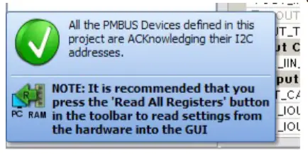 c. In the Toolbar, click the “R” (RAM to PC) icon to read the RAM from the LTC3880 and the LTC3883This reads the configuration from the RAM of LTC3883 and loads it into the GUI.
![]() d. If you want to change the output voltage to a different value, like 1.5V. In the Config tab, type in 1.5 in the VOUT_COMMAND box, like this:
d. If you want to change the output voltage to a different value, like 1.5V. In the Config tab, type in 1.5 in the VOUT_COMMAND box, like this:
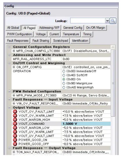
Then, click the “W” (PC to RAM) icon to write these register values to the LTC3880 and the LTC3883. After finishing this step, you will see the output voltage will change to 1.5V.
![]() If the write is successful, you will see the following message:
If the write is successful, you will see the following message:
 e. You can save the changes into the NVM. In the tool bar, click “RAM to NVM” button, as following
 f. Save the demo board configuration to a (*.proj) file. Click the Save icon and save the file. Name it whatever you want.
PARTS LIST
| ITEM | QTY | REFERENCE | PART DESCRIPTION | MANUFACTURER/PART NUMBER |
Required Circuit Components
| 1 | 4 | C1, C2, C28, C29 | CAP., X5R, 22µF, 25V, 10%,1210 | AVX, 12103D226KAT |
| 2 | 2 | C5, C30 | CAP., X5R, 1µF, 10V, 20%, 0603 | AVX, 0603ZD105MAT2A |
| 3 | 6 | C4, C10, C11, C16, C27, C36 | CAP., X5R, 1µF, 10V, 20%, 0402 | AVX, 0402ZD105MAT2A |
| 4 | 1 | C6 | CAP., X5R, 10µF, 10V, 20%, 0603 | SAMSUNG, CL10A106MP8NNNC |
| 5 | 3 | C3, C9, C26 | CAP., X7R, 0.1µF, 25V, 10%, 0603 | AVX, 06033C104KAT |
| 6 | 2 | C7, C8 | CAP., OS-CON, 330µF, 16V, 20% | SANYO, 16SVP330M |
| 7 | 20 | C12-C15, C17, C31-C35, C43-C52 | CAP., X5R, 100µF, 6.3V, 20%,1206 | TAYO YUDEN, JMK316BJ107ML-T |
| 8 | 2 | C18, C19 | CAP., POSCAP, 470µF, 2.5V, D2E | SANYO 2R5TPE470M9 |
| 9 | 2 | C22, C37 | CAP., X5R, 0.22µF, 16V, 20%, 0402 | TDK, C1005X5R1C224M |
| 10 | 1 | C23 | CAP., X7R, 1nF, 25V, 10%, 0402 | AVX, 04023C102KAT2A |
| 11 | 1 | C24 | CAP., NPO, 100pF,25V, 10%, 0402 | AVX,04023A101KAT2A |
| 12 | 1 | C25 | CAP., X5R, 10nF, 25V, 10%, 0402 | AVX, 04023D103KAT2A |
| 13 | 2 | L1, L2 | INDUCTOR, SMT POWER IND. 0.16µH | COILCRAFT., XAL7070-161ME |
| 14 | 1 | Q1 | TRANS GP SS PNP 40V SOT-23 | ON SEMI MMBT3906LT1G |
| 15 | 1 | Q3 | MOSFET P-CH 20V, 0.58A, SOT-23 | VISHAY, TP0101K-T1-E3 |
| 16 | 6 | R2, R11, R12, R16, R17, R30 | RES., CHIP, 0, 1%, 0402 | VISHAY, CRCW04020000Z0ED |
| 17 | 4 | R1, R13, R36, R66 | RES., CHIP, 0, 1%, 0603 | VISHAY, CRCW06030000Z0EA |
| 18 | 2 | R3, R15 | RES., CHIP, 10, 1%, 0603 | VISHAY, CRCW060310R0FKEA |
| 19 | 2 | R7, R19 | RES., CHIP, 10k, 1%, 0402 | VISHAY, CRCW040210K0FKED |
| 20 | 5 | R18, R20, R22, R24, R39 | RES., CHIP, 10k, 1%, 0603 | VISHAY, CRCW060310K0FKEA |
| 21 | 1 | R6 | RES., CHIP, 1, 1%, 0402 | VISHAY, CRCW04021R00FKED |
| 22 | 4 | R8, R9, R25, R27 | RES., CHIP, 825, 1%, 0402 | VISHAY, CRCW0402825RJNED |
| 23 | 1 | R14 | RES., CHIP, 6.81k, 1%, 0402 | VISHAY, CRCW04026K81FKED |
| 24 | 1 | R23 | RES., CHIP, 20k, 1%, 0402 | VISHAY,CRCW040220K0FKED |
| 25 | 1 | R28 | RES., CHIP, 17.8k, 1%, 0402 | VISHAY,CRCW040217K8FKED |
| 26 | 1 | R31 | RES., CHIP, 16.2k, 1%, 0603 | VISHAY, CRCW060316K2FKEA |
| 27 | 1 | R33 | RES., CHIP, 24.9k, 1%, 0603 | VISHAY, CRCW060324K9FKEA |
| 28 | 1 | R34 | RES., CHIP, 4.32k, 1%, 0603 | VISHAY, CRCW06034K32FKEA |
| 29 | 1 | R40 | RES., CHIP, 15.8k, 1%, 0603 | VISHAY, CRCW060315K8FKEA |
| 30 | 2 | U1, U3 | IC, HIGH FREQUENCY DrMOS MOUDLE | FAIRCHILD, FDMF6823A |
| 31 | 1 | U2 | IC, LTC3880EUJ, QFN 6mm ´ 6mm | LTC., LTC3880EUJ#PBF |
Additional Circuit Components
| 1 | 2 | CBYP1, CBYP2 | CAP., X7R, 0.01µF,16V, 10%, 0603 | AVX, 0603YC103KAT |
| 2 | 2 | COUT1, COUT2 | CAP., X5R, 10µF,25V, 20%,1206 | TDK, C3216X7R1E106M |
| 3 | 1 | C40 | CAP., X7R, 1µF, 16V, 10%, 1206 | AVX, 1206YC105KAT |
| 4 | 1 | C41 | CAP., X7R, 0.1µF, 25V, 10%, 0603 | AVX, 06033C104KAT |
| 5 | 1 | C39 | CAP., X5R, 1µF, 16V, 20%, 0805 | AVX, 0805YD105MAT |
| 6 | 0 | C20, C21, C53, C54 | CAP., POSCAP, 470µF, 2.5V, D2E | SANYO 2R5TPE470M9 |
| 7 | 1 | C38 | CAP., X5R, 2.2µF, 16V, 10%, 0805 | AVX, 0805YD225KAT |
| 8 | 1 | C42 | CAP., X5R, 10nF, 25V, 10%, 0603 | AVX, 06033D103KAT |
| 9 | 1 | C55 | CAP., X7R, 0.1µF,16V, 10%, 0603 | AVX, 0603YC104KAT |
| ITEM | QTY | REFERENCE | PART DESCRIPTION | MANUFACTURER/PART NUMBER |
| 10 | 1 | D1 | LED GREEN S-GW TYPE SMD | ROHM, SML-010FTT86L |
| 11 | 1 | D2 | LED RED S-TYPE GULL WING SMD | ROHM, SML-010VTT86L |
| 12 | 1 | D3 | DIODE, SCHOTTKY, SOD-323 | CENTRAL CMDSH-3TR |
| 13 | 1 | Q2 | MOSFET SPEED SRS 30V 30A LFPAK | RENESAS, RJK0305DPB-00#J0 |
| 14 | 1 | Q3 | MOSFET P-CH 20V 0.58A SOT-23 | VISHAY, TP0101K-T1-E3 |
| 15 | 1 | Q5 | MOSFET N-CH 60V 115MA SOT-23 | FAIRCHILD, 2N7002A-7-F |
| 16 | 7 | R54-R60 | RES., CHIP, 0, 1%, 0603 | VISHAY, CRCW06030000Z0EA |
| 17 | 1 | R51 | RES., CHIP, 10, 1%, 0603 | VISHAY, CRCW060310R0FKEA |
| 18 | 2 | R38, R48 | RES., CHIP, 10k, 1%, 0603 | VISHAY, CRCW060310K0FKEA |
| 19 | 2 | R43, R44, | RES., CHIP, 100k, 1%, 0603 | VISHAY, CRCW0603100KFKEA |
| 20 | 1 | R10 | RES., CHIP, 30, 1%, 2512 | VISHAY, CRCW251230R0FKEA |
| 21 | 0 | R21, R62, R63 (OPT) | RES., 0402 | |
| 22 | 0 | R4, R5, R26, R29, R32, R35 (OPT) | RES., 0603 | |
| 23 | 0 | R47 (OPT) | RES., 0805 | |
| 24 | 1 | R37 | RES., CHIP, 200, 1%, 0603 | VISHAY, CRCW0603200RFKEA |
| 25 | 1 | R41 | RESISTOR .010Ω 1W, 1% 2512 | PANASONIC, ERJ-M1WSF10MU |
| 26 | 1 | R42 | RES., CHIP, 127, 1%, 0603 | VISHAY, CRCW0603127RFKEA |
| 27 | 2 | R45, R46 | RES., CHIP, 4.99k, 1%, 0603 | VISHAY, CRCW06034K99FKEA |
| 28 | 1 | R49 | RES., CHIP, 6.19k, 1%, 0603 | VISHAY, CRCW06036K19FKEA |
| 29 | 1 | R50 | RES., CHIP, 3.4k, 1%, 0603 | VISHAY, CRCW06033K40FKEA |
| 30 | 2 | R52, R53 | RES., CHIP, 2k, 1%, 0603 | VISHAY, CRCW06032K00FKEA |
| 31 | 1 | U4 | IC, SERIAL EEPROM | MICROCHIP 24LC025-I/ST |
| 32 | 1 | U5 | IC, LT3029IMSE, MSOP, 16 PIN | LTC., LT3029IMSE#PBF |
Hardware
| 1 | 8 | E1, E2, E4, E6, E11, E12, E15, E16 | TESTPOINT, TURRET, .062″ | MILL-MAX, 2308-2-00-80-00-00-07-0 |
| 2 | 2 | J1, J2 | JACK, BANANA | KEYSTONE 575-4 |
| 3 | 2 | J3, J4 | STUD, TEST PIN | PEM KFH-032-10 |
| 4 | 4 | J3, J4(X2) | NUT, BRASS 10-32 | ANY #10-32 |
| 5 | 2 | J3, J4 | RING, LUG #10 | KEYSTONE, 8205, #10 |
| 6 | 2 | J3, J4 | WASHER, TIN PLATED BRASS | ANY #10 |
| 7 | 2 | J5, J7 | CONN, BNC, 5-PINS | CONNEX, 112404 |
| 8 | 1 | J6 | CONN HEADER 12POS 2mm STR DL PCB | FCI 98414-G06-12ULF |
| 9 | 1 | J8 | HEADER., DOUBLE ROW, RIGHT ANGLE 2 ´ 5 PIN | MILL-MAX 802-40-010-20-001000 |
| 10 | 1 | J9 | SOCKET, DOUBLE ROW, 2 ´ 5 PIN | MILL-MAX 803-43-010-20-001000 |
| 11 | 2 | JP1, JP2 | HEADER 3 PIN 0.079 SINGLE ROW | SULLIN, NRPN031PAEN-RC |
| 12 | 2 | JP1, JP2 | SHUNT | SAMTEC, 2SN-BK-G |
| 13 | 1 | SW | SWITCH SLIDE 1PDT 6VDC 0.3A SMT | C & K JS102011SAQN |
| 14 | 4 | STANDOFF | STANDOFF, SNAP ON | KEYSTONE_8831 |
| 15 | 1 | STENCIL | STENCIL |
SCHEMATIC DIAGRAM


Information furnished by Linear Technology Corporation is believed to be accurate and reliable. However, no responsibility is assumed for its use. Linear Technology Corporation makes no representation that the interconnection of its circuits as described herein will not infringe on existing patent rights.
DEMONSTRATION BOARD IMPORTANT NOTICE
Linear Technology Corporation (LT C ) provides the enclosed product(s) under the following AS IS conditions: This demonstration board (DEMO BOARD) kit being sold or provided by Linear Technology is intended for use for ENGINEERING DEVELOPMENT OR EVALUATION PURPOSES ONLY and is not provided by LT C for commercial use. As such, the DEMO BOARD herein may not be complete in terms of required design-, marketing-, and/or manufacturing-related protective considerations, including but not limited to product safety measures typically found in finished commercial goods. As a prototype, this product does not fall within the scope of the European Union directive on electromagnetic compatibility and therefore may or may not meet the technical requirements of the directive, or other regulations. If this evaluation kit does not meet the specifications recited in the DEMO BOARD manual the kit may be returned within 30 days from the date of delivery for a full refund. THE FOREGOING WARRANTY IS THE EXCLUSIVE WARRANTY MADE BY THE SELLER TO BUYER AND IS IN LIEU OF ALL OTHER WARRANTIES, EXPRESSED, IMPLIED, OR STATUTORY, INCLUDING ANY WARRANTY OF MERCHANTABILITY OR FITNESS FOR ANY PARTICULAR PURPOSE. EXCEPT TO THE EXTENT OF THIS INDEMNITY, NEITHER PARTY SHALL BE LIABLE TO THE OTHER FOR ANY INDIRECT, SPECIAL, INCIDENTAL, OR CONSEQUENTIAL DAMAGES. The user assumes all responsibility and liability for proper and safe handling of the goods. Further, the user releases LT C from all claims arising from the handling or use of the goods. Due to the open construction of the product, it is the user’s responsibility to take any and all appropriate precautions with regard to electrostatic discharge. Also be aware that the products herein may not be regulatory compliant or agency certified (FCC, UL, CE, etc.). No License is granted under any patent right or other intellectual property whatsoever. LT C assumes no liability for applications assistance, customer product design, software performance, or infringement of patents or any other intellectual property rights of any kind. LT C currently services a variety of customers for products around the world, and therefore this transaction is not exclusive. Please read the DEMO BOARD manual prior to handling the product. Persons handling this product must have electronics training and observe good laboratory practice standards. Common sense is encouraged. This notice contains important safety information about temperatures and voltages. For further safety concerns, please contact a LT C application engineer.
Mailing Address:
Linear Technology
1630 McCarthy Blvd.
Milpitas, CA 95035
Copyright © 2004, Linear Technology Corporation
Documents / Resources
 |
LINEAR TECHNOLOGY DC2088A DC Converter with Power System Management [pdf] Instruction Manual DC2088A, DC2088A DC Converter with Power System Management, DC Converter with Power System Management, Power System Management, System Management |


