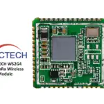
netvox R107H Wireless LoRa Module

Specifications
- Product: Wireless LoRa Module R107H
- Version Date: Preliminary 2024-03-20
- Hardware Version: V0.2 61R1076801 v02
Product Description
The RF module R107H includes LoRa RF function by NETVOX, a low power consumption transceiver based on the STM32WLE5 chip LoRaTM solution. It is designed to be SMD-mounted onto a host PCB,providing optimal RF performance at a low cost. The module occupies minimal board space and integrates easily into other devices without requiring RF expertise.
Applications
The R107H is suitable for various applications requiring long-range communication with low power consumption.
Electric Specifications
Performance:
- Power Output: 22 dBm (MAX)
- Outdoor Range: 10KM (MAX)
- RF Data Rate: LoRa 0.013 to 17.4 Kbit/s; FSK: 0.6 to 300Kbit/s
- Frequency Band: EU863-870, US902-928, AU915-928, KR920-923,AS923, IN865
- Modulation Techniques: LoRa
- Receiver Sensitivity: Varies
Pin Description
| Pin NO. | Pin Name | Pin Type | Description |
|---|
Mechanical Drawing and Dimensions
FAQ
Q: What is the maximum power output of the R107H module?
A: The maximum power output is 22 dBm.
Copyright
©Netvox Technology Co., Ltd.
This document contains proprietary technical information which is the property of NETVOX Technology and is issued in strict confidentiality and shall not be disclosed to others parties in whole or in parts without written permission of NETVOX TechnologyTechnology.
The specifications are subjected to change without prior notice.
History
| Version | Date | Note |
| Preliminary | 2024-03-20 | Initial Release |
Notes
Hardware version V 0. 2
61R1076801 v02
Product Description
The RF module R107H include LoRa rf function by NETVOX is low power consumption transceiver based on the STM32WLE5 chip LoRaTM solution.
The R107H is designed to be SMD-mounted onto a host PCB. SMD-mounting provides the best RF performance at the lowest cost. Additionally the R107H is designed to occupy minimal board space on the host PCB, which already includes plentiful interfacing ports and power management circuits. So it can be easily integrated into other device without the need for RF experience and expertise.
Applications
- Automated Meter Reading
- Smart City, Smart Agriculture , Smart Industry, IOT Application
- Wireless Alarm and Security Systems
- Industrial Monitoring and Control
- Long range Irrigation Systems
Key Features
- High performance and low power 32-bit ARM Cortex-M0 CPU
- 2562kbytes of flash memory
- Compact Form Factor: 24.5 x 16 x 2.5 mm
- 28 Pin Stamp Pad for PCB SMT mounting
- I/O port: UART/I2C/GPIO
- Temperature range: -25°C to +85°C
- Supply voltage: 1.8 ~ 3.6V
- Lora Frequency range: 863 – 928 MHz, ISM and SRD systems
- Transmitter high output power, programmable up to +22 dBm
- Transmitter low output power, programmable up to +15 dBm
- RX sensitivity: –123 dBm for 2-FSK (at 1.2 Kbit/s), –148 dBm for LoRa® (at 10.4 kHz, spreading factor 12)
- Modulation: LoRa®, (G)FSK, (G)MSK and BPSK
- Low-Power Wireless Systems with 7.8-kHz to 500-KHz Bandwidth
Electric Specifications
Performance
| Power out | 22 dBm (MAX) |
| Outdoor range | 10KM(MAX) |
| RF Data rate | LoRa:0.013 to 17.4 Kbit/s ;FSK:0.6 to 300 Kbit/s |
| Frequency Band | EU863-870,US902-928,AU915-928,KR920-923, AS923,IN865 |
| Modulation Techniques | LoRa®, (G)FSK, (G)MSK and BPSK |
| Receiver Sensitivity | –123 dBm for 2-FSK (at 1.2 Kbit/s),
–148 dBm for LoRa® (at 10.4 kHz, spreading factor 12) |
DC Characteristics
| Support Voltage | 3.3 V for lora:2.4V-3.6V |
| RX Current | 10.22mA (MAX) |
| TX Current | 142mA (MAX) |
| Standby SMPS mode | 1.05mA |
| Deep Sleep (including
internal RC oscillator) |
10uA |
Absolute Maximum Ratings
| Parameter | Min | Max | Unit |
| Supply voltage for 3.3V | -0.3 | 36 | V |
| Voltage on any pin | -0.3 | VCC+0.3 | V |
| Storage temperature | -40 | 105 | ℃ |
| Operating temperature | -25 | 85 | ℃ |

Block diagram

Pin Assignment

Figure 3 Pin assignment
Pin Description
| Pin NO. | Pin name | Pin type | Description |
| 1 | GND | Ground | GND |
| 2 | /RST | I | Hardware Active low chip reset |
| 3 | SWDIO | I/O | Programming and debug interface |
| 4 | SWCLK | I/O | Programming and debug interface |
| 5 | VCC | Power | 2.4V-3.6V DC power supply |
| 6 | PA8 | I/O | GPIO |
| 7 | PA10 | I/O | GPIO /UART1_ RX/ADC1 |
| 8 | PA9 | I/O | GPIO / UART1_TX |
| 9 | PB0 | I/O | GPIO / |
| 10 | PB2 | I/O | GPIO /ADC2 |
| 11 | PB12 | I/O | GPIO |
| 12 | PA11 | I/O | GPIO/ADC3 |
| 13 | PA12 | I/O | GPIO/ADC4 |
| 14 | GND | Ground | GND |
| 15 | GND | Ground | GND |
| 16 | GND | Ground | GND |
| 17 | PB6 | I/O | GPIO |
| 18 | PB7 | I/O | GPIO |
| 19 | PA3 | I/O | GPIO/UART2-RX |
| 20 | PA2 | I/O | GPIO/UART2-TX |
| 21 | PB4 | I/O | GPIO/ADC5 |
| 22 | PB3 | I/O | GPIO/ADC6 |
| 23 | PA15 | I/O | GPIO/ADC7 |
| 24 | PA5 | I/O | GPIO |
| 25 | PA6 | I/O | GPIO |
| 26 | VCC | Power | 2.4V-3.6V DC power supply |
| 27 | VCC | Power | 2.4V-3.6V DC power supply |
| 28 | GND | Ground | GND |
Debugging interface
Pin1~pin5 of the module are arranged for debugging interface.
Mechanical Drawing and Dimensions

Antenna and Range Considerations
The R107H module is delivered with an integrated antenna. This is highly recommended for most applications, as this gives a very compact solution containing all the critical RF parts within the module.
The radiation pattern from the antenna is similar to the donut-shaped obtained from a quarter wave antenna. That is, the maximum radiation is in the plane perpendicular to the length axis of the antenna. For best achievable radiation the module should be oriented so that the antenna is vertical.
The antenna should be kept more than 10 millimeters away from metallic or other conductive and dielectric materials. Any metallic enclosures would shield the antenna and reduce the communication range drastically. In applications where the module must be placed in a metallic enclosure, an external antenna would give best signal strength. The external antenna is attachable from the i PEX connector . The RF input/output is matched to 50 Ohm.
PCB Layout Recommendations
The figure 5 shows the proper layout footprint for the module. The footprint shown by figu re 6 is also fit for the PA module offered by NETVOX.
The area underneath the module should be covered with a sol i d ground plane.
And for greater flexibility and compatibility, the footprint shown by Figure 6 is strongly recommended to use.
Each ground pin
should be connected directly to the ground plane. In case the ground plane is on an inner layer of the PCB, via should be placed as close as possible to every ground pad of the module to create low impedance grounding. Unconnected pins should be soldered to the pads,and the pads should be left floating.
When using the module with on board ceramic chip antenna lying on the north east corner of the module, the area underneath the antenna should be kept open, and if possible extended in east and north direc tion as far as possible. Best possible placement of the module on your main PCB is in the far north east corner. Positioning to suit different application please refer to the figure 7.


For in circuit programming and debugging, the 10 pin interface (as following figure ) must be reserved in the mainboard PCB.

The 10 PIN respectively connects the module module’s PIN. Please see the table below for the detail.
| Interface PIN NO. | 1 | 2 | 3 | 4 | 5 |
| Module’s PIN | VCC | /RST | SWCLK | ||
| Interface PIN NO. | 6 | 7 | 8 | 9 | 10 |
| Module’s PIN | GND | SWDIO |
NOTE:
FCC Statement
This device complies with part 15 of the FCC Rules. Operation is subject to the following two conditions:
- This device may not cause harmful interference, and
- this device must accept any interference received, including interference that may cause undesired operation.
This equipment has been tested and found to comply with the limits for a Class B digital device,pursuant to part 15 of the FCC Rules. These limits are designed to provide reasonable protection against harmful interference in a residential installation. This equipment generates,uses and can radiate radio frequency energy and, if not installed and used in accordance with the instructions, may cause harmful interference to radio communications. However, there is no guarantee that interference will not occur in a particular installation. If this equipment does cause harmful interference to radio or television reception, which can be determined by turning the equipment off and on, the user is encouraged to try to correct the interference by one or more of the following measures:
- Reorient or relocate the receiving antenna.
- Increase the separation between the equipment and receiver.
- Connect the equipment into an outlet on a circuit different from that to which the receiver is connected.
- Consult the dealer or an experienced radio/TV technician for help.
Caution: Any changes or modifications not expressly approved by the party responsible for compliance could void the user’s authority to operate the equipment.
This equipment complies with FCC radiation exposure limits set forth for an uncontrolled environment. This transmitter must not be co-located or operating in conjunction with any other antenna or transmitter.
IC Statement:
This device complies with Industry Canada’ s licence – exempt RSSs. Operation is subject to the following two conditions:
- This device may not cause interference; and
- This device must accept any interference, including interference that may cause undesired operation of the device.
The host product shall be properly labelled to identify the modules within the host product.
The ISED certification label of a module shall be clearly visible at all times when installed in the host product; otherwise,the host product must be labelled to display the ISED certification number for the module, preceded by the word “contains” or similar wording expressing the same meaning, as follows:
Contains IC: 8984A-R107H
Integration instructions for host product manufacturers according to KDB 996369 D03 OEM
Manual v01
List of applicable FCC rules
CFR 47 FCC PART 15 SUBPART C has been investigated. It is applicable to the modular transmitter
Specific operational use conditions
This module is stand-alone modular. If the end product will involve the Multiple simultaneously transmitting condition or different operational conditions for a stand-alone modular transmitter in a host, host manufacturer have to consult with module manufacturer for the installation method in end system.
Limited module procedures
Not applicable
Trace antenna designs
Not applicable
RF exposure considerations
This equipment complies with FCC radiation exposure limits set forth for an uncontrolled environment. This equipment should be installed and operated with minimum distance 5mm between the radiator & your body.
Antennas
This radio transmitter R107H has been approved by Federal Communications Commission to operate with the antenna types listed below, with the maximum permissible gain indicated.
Antenna types not included in this list that have a gain greater than the maximum gain indicated for any type listed are strictly prohibited for use with this device.
| Antenna No. | Operate frequency band | Antenna Type | Maximum antenna gain |
| Antenna 1 | 902MHz~928MHz | FPC Antenna | 0.78 |
Label and compliance information
The final end product must be labeled in a visible area with the following” Contains FCC ID:NRH-LR-R107H”.
- Information on test modes and additional testing requirements Host manufacturer is strongly recommended to confirm compliance with FCC requirements for the transmitter when the module is installed in the host.
- Additional testing, Part 15 Subpart B disclaimer Host manufacturer is responsible for compliance of the host system with module installed with all other applicable requirements for the system such as Part 15 B.
Documents / Resources
 |
netvox R107H Wireless LoRa Module [pdf] Owner's Manual R107H, R107H Wireless LoRa Module, Wireless LoRa Module, LoRa Module, Module |
 |
netvox R107H Wireless LoRa Module [pdf] Owner's Manual LR-R107H, LRR107H, NRH-LR-R107H, NRHLRR107H, R107H Wireless LoRa Module, R107H, Wireless LoRa Module, LoRa Module, Module |