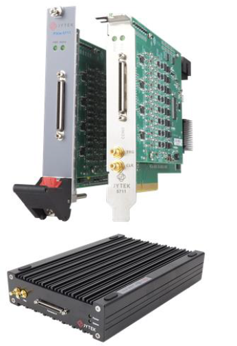
JYTEK JY-5710 Series Analog Output Function Modules
Specifications
- Model: JY5710 Series
- Channels: Up to 32 analog output channels
- Resolution: 16 bits
- Maximum Update Rate: 2MS/s
- Digital Input/Output: 3 lines
Product Usage Instructions
Overview
The JY5710 Series is a family of Analog Output function modules that can run on PCIe, PXIe, TXI (Thunderbolt), and USB buses. Depending on the model number, the 5710 series provides different AO channels and sampling rates.
Main Features
DMA for data transfers: Enables efficient data transfer.
Learn by Example
JYTEK provides sample programs for this device. Download the sample programs from the JYTEK website. Access JYPEDIA for additional information and search for JY5710 Examples.zip.
FAQ
- Q: Where can I find the latest offerings for the JY5710 series?
- A: Please check with JYTEK for the latest JY5710 series offerings.
- Q: What is the maximum update rate for the JY5711 module?
- A: The JY5711 module features a maximum update rate of 2MS/s.
Introduction
This chapter presents the information how to use this manual and how to quick start if you are already familiar with Microsoft Visual Studio and C# programming language.
Overview
The JY5710 Series is a family of Analog Output function modules, which can run on PCIe, PXIe, TXI (Thunderbolt) and USB buses. Depending on the model number, a 5710 series provide different AO channels, sampling rate.
JY5711 features up to 32 channels analog output module with 16 bits resolution and maximum update rate to 2MS/s, 3 lines of digital input/output.
Please check with JYTEK for the latest JY5710 series offering.
Main Features
- High accuracy: 0.02%
- 32 channels of voltage output
- 16 bits DAC
- Output range: ±10 V
- Maximum update rate
- 8 channels (2 MS/s/ch per bank)
- 32 channels: 1 MS/s
- Output current drive: ±10 mA
- Overdrive current:15 mA
- 8M samples FIFO buffer size per channel
- DMA for data transfers
Abbreviations
- AO: Analog Output
- DI: Digital Input
- DO: Digital Output
- DAC: Digital-to-Analog Conversion
- PFI: Programmable Function Interface
- SE: Single-Ended
- PPM: Parts Per Million
Learn by Example
JYTEK has added Learn by Example in this manual. We provide many sample programs for this device. Please download the sample programs for this device. You can download a JYPEDIA excel file from our web www.jytek.com . Open JYPEDIA and search for JY5710 in the driver sheet, select JY5710 Examples.zip. In addition to the download information, JYPEDIA also has a lot of other valuable information, JYTEK highly recommend you use this file to obtain information from JYTEK. 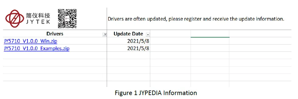
In a Learn by Example section, the sample program is in bold style such as Analog Output–>WinForms AO Continuous Wrapping Soft Trigger; the property name in the sample program is also in bold style such as Samples To Update the technical names used in the manual is in italic style such as Update Rate. You can easily relate the property names in the example program with the manual documentation.
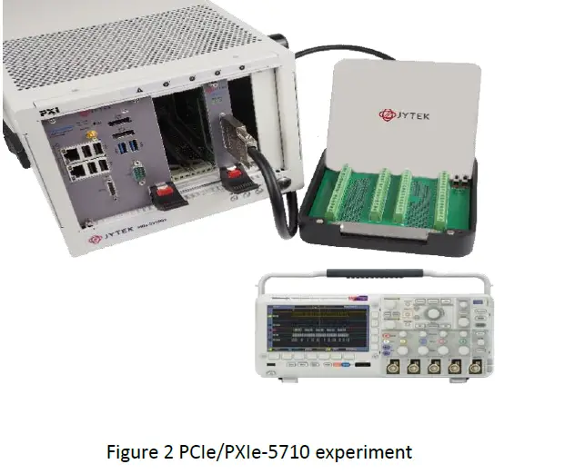
In an Learn by Example section, the experiment is set up as follow. A PCIe/PXIe-5710 card is plugged in a PXI Chassis. The PCIe/PXIe-5710 is connected to a TB-68 terminal block. A Oscilloscope is also connected to the same terminal block as shown Figure 2.
 Hardware Specifications
Analog Output Specifications
| Number of channels | 32 ch | |
| Resolution | 16 bits | |
| DNL | ±1 LSB | |
| Unscaled data format | Signed integer (-32768 to 32767) | |
| Monotonicity | 16 bits | |
| Clock | 200 MHz | |
| Maximum update rate | ||
| 1 channel | 2 MS/s | |
| 8 channels (1 channel per bank)* | 2 MS/s | |
| 32 channels | 1 MS/s | |
| Output range | ±10 V | |
| Output coupling | DC | |
| Output impedance | 0.2 Ω | |
| Output current drive | ±10 mA | |
| Overdrive protection | ±15 V | |
| Overdrive current | 15 mA | |
| Power-on state | ±200 mV | |
| FIFO buffer size | 8M Samples per channel | |
| Data transfers | DMA | |
| AO waveform modes |
|
|
| Slew rate | 20 V/µs | |
| Noise | 400 μVrms, DC to 1 MHz | |
| AO update glitch Glitch energy | 5 nVs | |
| Channel crosstalk | -65 dB | |
| Reference clock | PXIe_DSTARA, PXIe_DSTARB, PXIe_CLK100 | |
| External sample clock | PFI, PXI_TRIG | |
| Trigger source | Digital, Software | |
| Trigger type | Start Trigger | |
| Digital trigger source | PFI, PXI_TRIG | |
| * Each bank consists of four AO channels using two DACs. Any channels being used within a single bank will update simultaneously. | ||
Table 1 Analog Output Specifications
AO Accuracy
| JY5711 AO Basic Accuracy = ±(% of Output+% of Range) | ||||||||
| Nominal Range (V) | 24 Hour | Tcal ±1C° | 90 Days | Tcal ± 5° | 24 Hr Full- Scale Accuracy | 90 Days Full-Scale Accuracy | ||
| 10 | 0.003 | + | 0.005 | 0.012 | + | 0.008 | 790 uV | 2000 uV |
Table 2 Analog Output Basic Accuracy
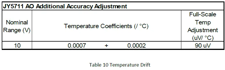
| JY5711 AO Additional Accuracy Adjustment | ||
| Nominal Range (V) | Temperature Coefficients (/ °C) | Full-Scale Temp Adjustment
(uV/ °C) |
| 10 | 0.0007 + 0.0002 | 90 uV |
Table 3 Analog Output Additional Accuracy
Digital IO / PFI Specifications
Static Characteristics
| Number of channels | 3 DIO |
| Ground reference | DGND |
| Direction control | Each terminal individually
programmable as input or output |
| Pull-down resistor | 50 kΩ typical |
| Input voltage protection | ±15 V |
PFI Functionality
| Number of channels | 3 |
| External digital trigger interface | Trigger voltage 3.3 V TTL;
Trigger edge: Rising/Falling |
| Initial state | Input |
Recommended Operating Conditions
| Minimum Input high voltage (VIH) | 2.2 V |
| Maximum Input high voltage (VIH) | 5.25 V |
| Minimum Input low voltage (VIL) | 0 V |
| Maximum Input low voltage (VIL) | 0.8 V |
| Maximum Output high current (IOH) | -16 mA |
| Maximum Output low current (IOL) | 16 mA |
Table 4 Digital IO / PFI Specifications
Bus and Power Specification
Bus Interface
| Form factor | x4 PXI Express peripheral module |
| Slot compatibility | x1 and x4 PXI Express or PXI Express hybird slots |
Power Requirements
| 3.3 V: | 3.0 W |
| +12 V: | 14.0 W |
Table 5 Bus and Power Specification
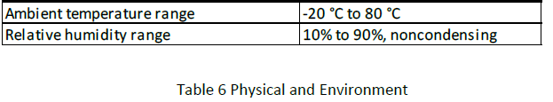
Physical and Environment
Operating Environment

Storage Environment
Front Panel and Pin Definition
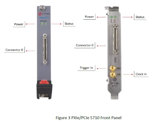
PCIe/PXIe-5710 series boards are connected to outside signals by one 68-pin cable for the 32 channel configurations, Table 7 shows the pin definitions of PCIe/PXIe-5711 .
| Connector 0 | |||
| Pin | Signal Name | Pin | Signal Name |
| 1 | PFI0/DIO_0 | 35 | DGND |
| 2 | PFI1/DIO_1 | 36 | PFI2/DIO_2 |
| 3 | AO_0 | 37 | AO_GND |
| 4 | AO_1 | 38 | AO_GND |
| 5 | AO_2 | 39 | AO_GND |
| 6 | AO_3 | 40 | AO_GND |
| 7 | AO_4 | 41 | AO_GND |
| 8 | AO_5 | 42 | AO_GND |
| 9 | AO_6 | 43 | AO_GND |
| 10 | AO_7 | 44 | AO_GND |
| 11 | AO_8 | 45 | AO_GND |
| 12 | AO_9 | 46 | AO_GND |
| 13 | AO_10 | 47 | AO_GND |
| 14 | AO_11 | 48 | AO_GND |
| 15 | AO_12 | 49 | AO_GND |
| 16 | AO_13 | 50 | AO_GND |
| 17 | AO_14 | 51 | AO_GND |
| 18 | AO_15 | 52 | AO_GND |
| 19 | AO_16 | 53 | AO_GND |
| 20 | AO_17 | 54 | AO_GND |
| 21 | AO_18 | 55 | AO_GND |
| 22 | AO_19 | 56 | AO_GND |
| 23 | AO_20 | 57 | AO_GND |
| 24 | AO_21 | 58 | AO_GND |
| 25 | AO_22 | 59 | AO_GND |
| 26 | AO_23 | 60 | AO_GND |
| 27 | AO_24 | 61 | AO_GND |
| 28 | AO_25 | 62 | AO_GND |
| 29 | AO_26 | 63 | AO_GND |
| 30 | AO_27 | 64 | AO_GND |
| 31 | AO_28 | 65 | AO_GND |
| 32 | AO_29 | 66 | AO_GND |
| 33 | AO_30 | 67 | AO_GND |
| 34 | AO_31 | 68 | AO_GND |
Table 7 5710 Pin Definition
Notes to Legend in the Pin Definitions
| AO_GND | Analog Output Reference Ground |
| AO<0..31> | Analog Output channel |
| D_GND | Digital Signal Reference Ground |
| PFI<0..2> | Programmable Function Interface |
Table 8 Notes to Legend
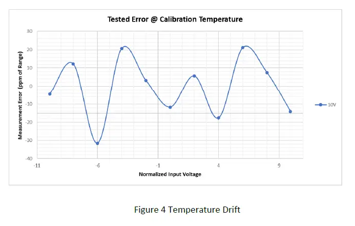
Performance and Tests
AO Accuracy
The best AO accuracy is limited by two factors: Total Gain Error and Total Offset Error as shown in the following table. The PCIe/PXIe-5710 device is first calibrated.
| JY5711 AO Basic Accuracy = ±(% of Output+% of Range) | ||||||||
| Nominal Range (V) | 24 Hour | Tcal ±1C° | 90 Days | Tcal ± 5° | 24 Hr Full- Scale Accuracy | 90 Days Full-Scale Accuracy | ||
| 10 | 0.003 | + | 0.005 | 0.007 | + | 0.011 | 790 uV | 1800 uV |
Temperature Drift
The temperature change will affect the AO accuracy by the gain error and offset error. The typical gain error and offset error of PCIe/PXIe-5710 are show below.
Crosstalk
| Reference Channel | Tested Channel | Crosstalk(dB at 100 KHz) |
| 0 | 1 | -71.8 |
| 0 | 15 | -71.4 |
| 0 | 16 | -70.4 |
| 1 | 2 | -71.8 |
| 6 | 7 | -71.4 |
| 6 | 22 | -70.9 |
| 10 | 11 | -72.1 |
| 16 | 17 | -67.2 |
| 31 | 30 | -71.6 |
Software
System Requirements
PCIe/PXIe-5710 boards can be used in a Windows or a Linux operating system.
- Microsoft Windows: Windows 7 32/64 bit, Windows 10 32/64 bit.
- Linux Kernel Versions: There are many Linux versions. It is not possible JYTEK can support and test our devices under all different Linux versions. JYTEK will at the best support the following Linux versions.
| Linux Version |
| Ubuntu LTS |
| 16.04: 4.4.0-21-generic(desktop/server) |
| 16.04.6:4.15.0-45-generic(desktop) 4.4.0-142-generic(server) |
| 18.04: 4.15.0-20-generic(desktop) 4.15.0-91-generic(server) |
| 18.04.4:5.3.0-28-generic (desktop) 4.15.0-91-generic(server) |
| Localized Chinese Version |
| V7.0(Build61): 3.10.0-862.9.1.nd7.zx.18.x86_64 |
| V7.0U6: 3.10.0-957.el7.x86_64 |
Table 12 Supported Linux Versions
System Software
When using the PCIe/PXIe-5710 in the Window environment, you need to install the following software from Microsoft website:
Microsoft Visual Studio Version 2015 or above,
- NET Framework version is 4.0 or above.
- NET Framework is coming with Windows 10. For Windows 7, please check .NET Framework version and upgrade to 4.0 or later version.
Given the resources limitation, JYTEK only tested PCIe/PXIe-5710 be with .NET Framework 4.0 with Microsoft Visual Studio 2015. JYTEK relies on Microsoft to maintain the compatibility for the newer versions.
C# Programming Language
All JYTEK default programming language is Microsoft C#. This is Microsoft recommended programming language in Microsoft Visual Studio and is particularly suitable for the test and measurement applications. C# is also a cross platform programming language.
PCIe/PXIe-5710 Series Hardware Driver
- After installing the required application development environment as described above, you need to install the PCIe/PXIe-5710 hardware driver.
- JYTEK hardware driver has two parts: the shared common driver kernel software (FirmDrive) and the specific hardware driver.
- Common Driver Kernel Software (FirmDrive): FirmDrive is the JYTEK’s kernel software for all hardware products of JYTEK instruments. You need to install the FirmDrive software before using any other JYTEK hardware products. FirmDrive only needs to be installed once. After that, you can install the specific hardware driver.
- Specific Hardware Driver: Each JYTEK hardware has a C# specific hardware driver. This driver provides rich and easy-to-use C# interfaces for users to operate various PCIe/PXIe-5710 function. JYTEK has standardized the ways which JYTEK and other vendor’s DAQ boards are used by providing a consistent user interface, using the methods, properties and enumerations in the object-oriented programming environment. Once you get yourself familiar with how one JYTEK DAQ card works, you should be able to know how to use all other DAQ hardware by using the same methods.
- Note that this driver does not support cross-process, and if you are using more than one function, it is best to operate in one process.
Install the SeeSharpTools from JYTEK
To efficiently and effectively use PCIe/PXIe-5710 boards, you need to install a set of free C# utilities, SeeSharpTools from JYTEK. The SeeSharpTools offers rich user interface functions you will find convenient in developing your applications. They are also needed to run the examples come with PCIe/PXIe-5710 hardware. Please register and download the latest SeeSharpTools from our website, www.jytek.com .
Running C# Programs in Linux
Most C# written programs in Windows can be run by MonoDevelop development system in a Linux environment. You would develop your C# applications in Windows using Microsoft Visual Studio. Once it is done, run this application in the MonoDevelop environment. This is JYTEK recommended way to run your C# programs in a Linux environment.
If you want to use your own Linux development system other than MonoDevelop, you can do it by using our Linux driver. However, JYTEK does not have the capability to support the Linux applications. JYTEK completely relies upon Microsoft to maintain the cross-platform compatibility between Windows and Linux using MonoDevelop.
Operating PCIe/PXIe-5710
- This chapter provides the operation guides for PCIe/PXIe-5710, including AO, DI, DO, etc.
- JYTEK provides extensive examples, on-line help and documentation to assist you to operate the PCIe/PXIe-5710 board. JYTEK strongly recommends you go through these examples before writing your own application. In many cases, an example can also be a good starting point for a user application.
Quick Start
- After you have installed the driver software and the SeeSharpTools, you are ready to use Microsoft Visual Studio C# to operate the PCIe/PXIe-5710 products.
- If you are already familiar with Microsoft Visual Studio C#, the quickest way to use PCIe/PXIe-5710 boards is to go through our extensive examples. We provide source code of our examples. In many cases, you can modify the source code and start to write your applications.
- We also provide Learn by Example in the following sections. These examples will help you navigate and learn how to use this PCIe/PXIe-5710.
AO Operations
The PCIe/PXIe-5710 AO provides 16-bit simultaneous outputs. The analog output has three modes of operation: Finite, Continuous Wrapping, and Continuous No Wrapping.
Finite Output
The finite output requires the user to write a piece of data. After starting the AO, it starts to output the written data until the output is completed.
Learn by Example 5.2.1
- Connect the PCIe/PXIe-5710 AO Ch0 (AO_0, Pin #3) to the probe tip of the oscilloscope, and AO ground (AO_GND, Pin #37) is connected to the grounding clip of the oscilloscope.
- PCIe/PXIe-5710 sends an analog signal through (AO_0, AO_GND) and reads the signal on an oscilloscope.
- Open Analog Output–>Winform AO Finite, set the following numbers as shown
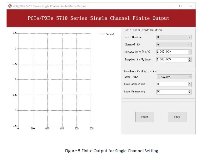
Click Start to generate a Sine Wave. The generated signal is shown below
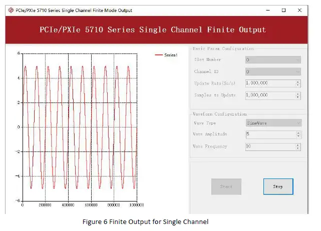
The image on the oscilloscope is shown in the figure

The analog signal is successfully generated by PCIe/PXIe-5710.
Continuous No Wrapping Output
The continuous acyclic output needs to write a piece of data before starting the AO. After the AO starts, user needs to continuously write new data to ensure the continuous output of the AO.
Learn by Example 5.2.1
- Connect the PCIe/PXIe-5710 AO Ch0 (AO_0, Pin #3) to the probe tip of the oscilloscope, and AO ground (AO_GND, Pin #37) is connected to the grounding clip of the oscilloscope.
- PCIe/PXIe-5710 sends an analog signal through (AO_0, AO_GND) and reads the signal on an oscilloscope.
- Open Analog Output–>Winform AO Continuous No Wrapping, set the following numbers as shown:
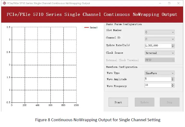
- In no wrapping analog output you can change the parameter of the signal whenever you want in Waveform Configuration when generating the wave. After the configuration you should click Update to apply the changes.
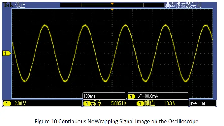
Click Start to generate a sinewave first. The result is shown below.

The image on the oscilloscope is shown in the figure
Now change the Wave Type to Square wave and click Update to generate it. The result is shown below.
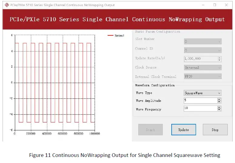
The image on the oscilloscope is shown in the figure
The analog signal is successfully generated by PCIe/PXIe-5710
Continuous Wrapping Output
The continuous loop output first writes a piece of data before starting the AO. After the AO starts, the board will repeatedly output this data until user sends a stop command.
Learn by Example 5.2.1
- Connect the PCIe/PXIe-5710 AO Ch0 (AO_0, Pin #3) to the probe tip of the oscilloscope, and AO ground (AO_GND, Pin #37) is connected to the grounding clip of the oscilloscope.
- PCIe/PXIe-5710 sends an analog signal through (AO_0, AO_GND) and reads the signal on an oscilloscope.
- Open Analog Output–>Winform AO Continuous Wrapping, set the following numbers as shown:
Click Start to generate the signal. The result is shown below.
The image on the oscilloscope is shown in the figure
The analog signal is successfully generated by PCIe/PXIe-5710.
Trigger Source
There are 3 trigger types: Immediate trigger, Software trigger, and Digital trigger. The trigger type is a property and set by driver software.
Immediate trigger
This trigger mode does not require configuration and is triggered immediately when an operation starts. The operation can be AO, DI, DO etc.
Learn by Example 5.2.1
- PCIe/PXIe-5710 AO Ch0 (AO_0, pin # 3) and AO Ch1 (AO_1, pin # 4) are connected to the probe tips of channel 1 and channel 2 of oscilloscope respectively. Connect AO ground (AO_GND, pin #37) to the ground clips of oscilloscope channels 1 and 2.
- PCIe/PXIe-5710 sends an analog signal through (AO_0,AO_GND)、(AO_1, AO_GND)and reads the signal on an oscilloscope.
- Open Analog Output–>Winform AO Continuous Wrapping Multichannel, set the following numbers as shown:

Click Start, the result is shown below.
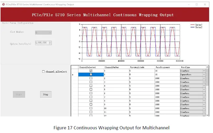
The image on the oscilloscope is shown in the figure
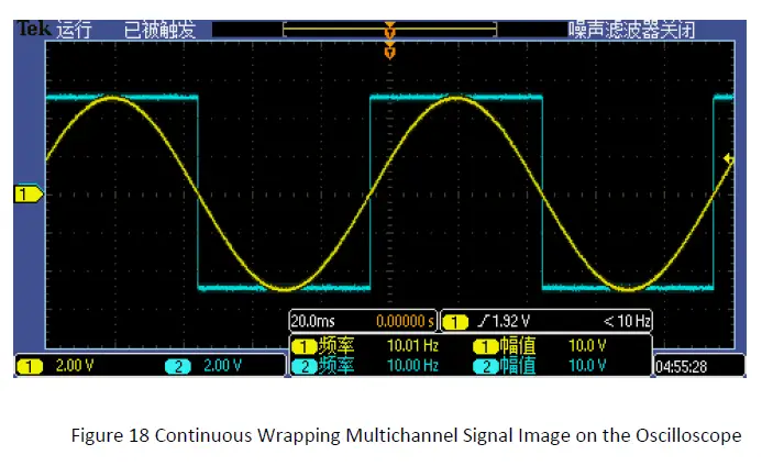
PCIe/PXIe-5710 multi-channel analog signal was successfully generated.
Software Trigger
A software trigger must be configured by the driver software. The trigger starts when a trigger software routine is called.
Learn by Example 5.3.2
- Connect the PCIe/PXIe-5710 AO Ch0 (AO_0, Pin #3) to the probe tip of the oscilloscope, and AO ground (AO_GND, Pin #37) is connected to the grounding clip of the oscilloscope.
- PCIe/PXIe-5710 sends an analog signal through (AO_0, AO_GND) and reads the signal on an oscilloscope.
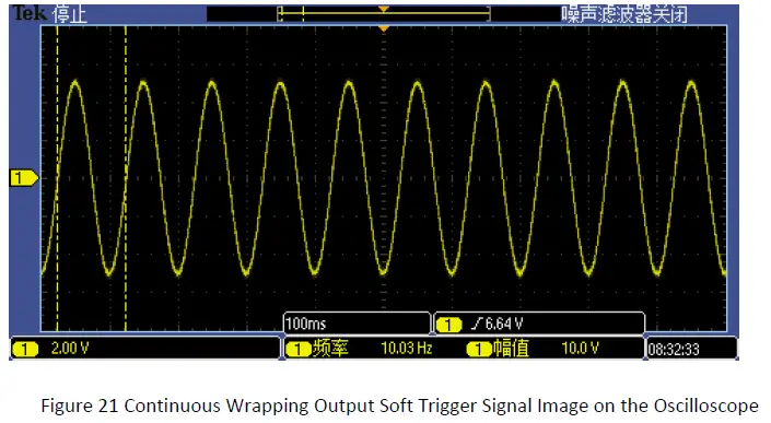
- Open Analog Output–>Winform AO Continuous Wrapping Soft Trigger, set the following numbers as shown:
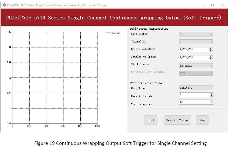
- Click Start to run the task.
- Data will not be acquired until there is a positive signal from Software Trigger when Send Soft Trigger is clicked.
- After sending the trigger signal, the result will be like this:
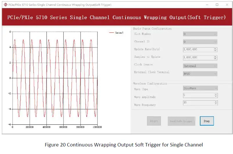
The image on the oscilloscope is shown in the figure
External Digital Trigger
PCIe/PXIe-5710 supports different external digital trigger sources from PXI Trigger bus (PXI_TRIG<0..7>), and PFI. The high pulse width of digital trigger signal must be longer than 20 ns for effective trigger. The module will monitor the signal on digital trigger source and wait for the rising edge or falling edge of digital signal which depending on the set trigger condition, then cause the module to acquire the data as shown in Figure 22. 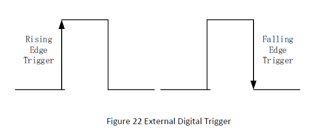
Learn by Example 5.2.1
- Connect the PCIe/PXIe-5710 AO Ch0 (AO_0, Pin #3) to the probe tip of the oscilloscope, and AO ground (AO_GND, Pin #37) is connected to the grounding clip of the oscilloscope.
- The positive connector of function generator is connected to the digital trigger source(PFI0, Pin #1)of PCIe/PXle-5710, and the negative connector is connected to the digital ground(DGND, Pin #35).Set up a squarewave signal (f=4Hz, Vpp=5v).
- Open Analog Output–>Winform AO Continuous Wrapping Digital Trigger, set the following numbers as shown:
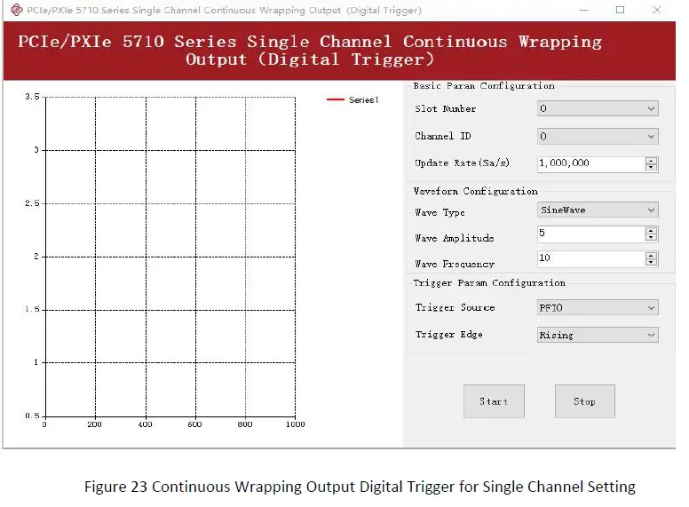
- Trigger Source must match the pin on 5710.
- There are two Trigger Edge: Rising and Falling.
- Click Start and the result shows below:
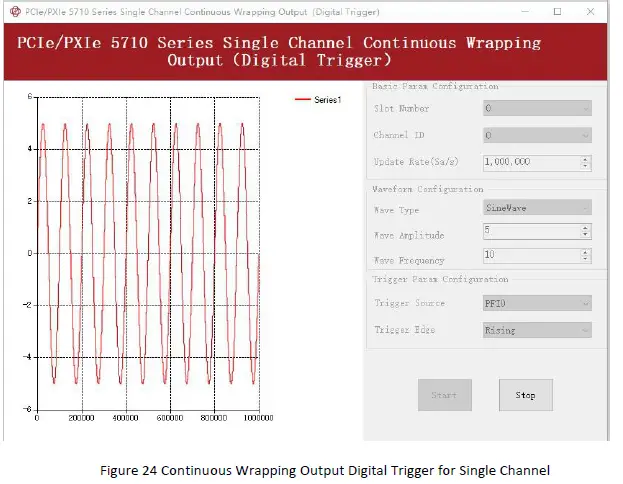
The image on the oscilloscope is shown in the figure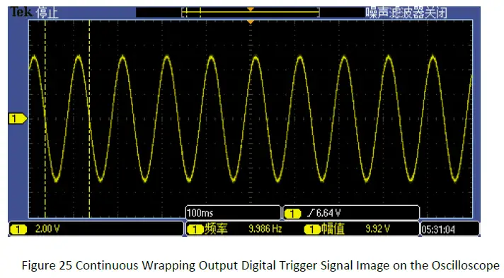
Since the square wave is used for the digital trigger source, when a rising edge of the square wave occurs, the digital trigger will be activated, and the data generation will start.
Digital I/O Operations
The PCIe/PXIe-5710 provides powerful programmable digital I/O functions.
Static DI/DO
Programmable I/O supports static TTL, 3 lines(0,1,2).User can access these I/O information through software polling.
Learn by Example 5.4.1
- In this example PCIe/PXIe-5710 outputs a digital signal by its DO function and reads it back by its DI function.
- Connect the PCIe/PXIe-5710 DIO_0/PFI0(pin #1) and DIO_1/PFI1(pin #2)
- Open the first program Digital Output–>Winform DO Single Point.
- Select line 0 for Digital Output, Set DO0 in High-Level positions, make sure all other lines are in Low-Level positions. Click Start to generate the High-Levels as shown.
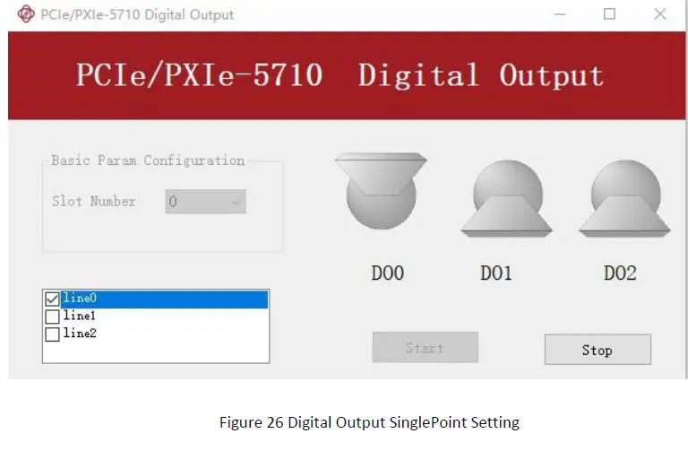
- Open the second program Digital Input–>Winform DI Single Point.
- Select line 1 for Digital Input as shown, and click Start. The result is shown below.

The result matches the high and low levels set before.
System Synchronization Interface (SSI) for PCIe Modules
The synchronization between PCIe modules are handled differently from the PXIe synchronization, it is implemented by the system synchronization interface (SSI). SSI is designed as a bidirectional bus and it can synchronize up to four PCIe modules. One PCIe module is designated as the master module and the other PCIe modules are designated as the slave modules. 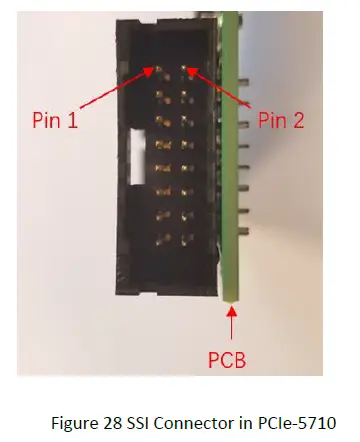
| Pin | Signal Name | Signal Name | Pin |
| 1 | PXI_TRIG0 | GND | 2 |
| 3 | PXI_TRIG1 | GND | 4 |
| 5 | PXI_TRIG2 | GND | 6 |
| 7 | PXI_TRIG3 | GND | 8 |
| 9 | PXI_TRIG4 | GND | 10 |
| 11 | PXI_TRIG5 | GND | 12 |
| 13 | PXI_TRIG6 | GND | 14 |
| 15 | PXI_TRIG7 | GND | 16 |
Table 13 SSI Connector Pin Assignment for PCIe-5710
DIP Switch in PCIe-5710
PCIe-5710 series modules have a DIP switch. The card number can be adjusted manually by changing the DIP switch setting, which is used to identify the boards with different slot positions.
For example, if you want to set the card number to 3, you could turn the position 2 and 1 of the DIP switch to the ON position and the orthers to OFF. See below for details.
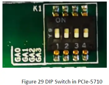
| Position 4
(GA3) |
Position 3
(GA2) |
Position 2
(GA1) |
Position 1
(GA0) |
|
| Slot 0 | 0 | 0 | 0 | 0 |
| Slot 1 | 0 | 0 | 0 | 1 |
| Slot 2 | 0 | 0 | 1 | 0 |
| Slot 3 | 0 | 0 | 1 | 1 |
| Slot 4 | 0 | 1 | 0 | 0 |
| Slot 5 | 0 | 1 | 0 | 1 |
| Slot 6 | 0 | 1 | 1 | 0 |
| Slot 7 | 0 | 1 | 1 | 1 |
| Slot 8 | 1 | 0 | 0 | 0 |
| Slot 9 | 1 | 0 | 0 | 1 |
| Slot 10 | 1 | 0 | 1 | 0 |
| Slot 11 | 1 | 0 | 1 | 1 |
| Slot 12 | 1 | 1 | 0 | 0 |
| Slot 13 | 1 | 1 | 0 | 1 |
| Slot 14 | 1 | 1 | 1 | 0 |
| Slot 15 | 1 | 1 | 1 | 1 |
| Note: OFF=0/ ON=1 | ||||
Table 14 Relationship between switch position and slot number
Calibration
PCIe/PXIe-5710 Series boards are pre calibrated before the shipment. We recommend you recalibrate PCIe/PXIe-5710 board periodically to ensure the measurement accuracy. A commonly accepted practice is one year. If for any reason, you need to recalibrate your board, please contact JYTEK.
Using PCIe/PXIe-5710 in Other Software
While JYTEK’s default application platform is Visual Studio, the programming language is C#, we recognize there are other platforms that are either becoming very popular or have been widely used in the data acquisition applications. Among them are Python, C++ and LabVIEW. This chapter explains how you can use PCIe/PXIe-5710 DAQ card using one of this software.
Python
JYTEK provides and supports a native Python driver for PCIe/PXIe-5710 boards. There are many different versions of Python. JYTEK has only tested in C Python version 3.5.4. There is no guarantee that JYTEK python drivers will work correctly with other versions of Python.
If you want to be our partner to support different Python platforms, please contact us.
C++
JYTEK internally uses our C++ drivers to design the C# drivers. We recommend our customers to use C# drivers because C# platform deliver much better efficiency and performance in most situations. We also make our C++ drivers available. However, due to the limit of our resources, we do not actively support C++ drivers. If you want to be our partner to support C++ drivers, please contact us.
LabVIEW
LabVIEW is a software product from National Instruments. JYTEK provides LabVIEW interface to PCIe/PXIe-5710 boards. You can download the LabVIEW drivers from our website. While JYTEK does not support LabVIEW applications, we may recommend you to a third party who can assist you to interface your LabVIEW with our PCIe/PXIe-5710 boards. We can also recommend you if you want to convert your LabVIEW applications to C# based applications.
About JYTEK
JYTEK China
Founded in June, 2016, JYTEK China is a leading Chinese test & measurement company, providing complete software and hardware products for the test and measurement industry. The company is a joint venture between Adlink Technologies and a group of experienced professionals form the industry. JYTEK independently develop the software and hardware products and is entirely focused on the Chinese market. Our Shanghai headquarters and production service center have regular stocks to ensure timely supply; we have R&D centers in Xi’an and Chongqing to develop new products; we also have highly trained direct technical sales representatives in Shanghai, Beijing, Tianjin, Xi’an, Chengdu, Nanjing, Wuhan, Haerbin, and Changchun. We also have many partners who provide system level support in various cities.
JYTEK Hardware Products
According to JYTEK’s agreement with our equity partner Ad link Technologies, JYTEK’s hardware is manufactured by the state-of-art manufacturing facility located in Shanghai Zhanjiang Hi-Tech Park. Ad link has over 20 years of the world-class low-volume and high-mix manufacturing expertise with ISO9001-2008, China 3C, UL, ROHS, TL9000, ISO-14001, ISO-13485 certifications. Its 30,000 square meters facilities and three high-speed Panasonic SMT production lines can produce 60,000 pieces boards/month; it also has full supply chain management – planning, sweeping, purchasing, warehousing and distribution. Ad link’s manufacturing excellence ensures JYTEK’s hardware has word-class manufacturing quality.
One core technical advantage is JYTEK’s pursue for the basic and fundamental technology excellence. JYTEK China has developed a unique PCIe, PXIe, USB hardware driver architecture, Firm Drive, upon which many our future hardware will be based.
In addition to our own developed hardware, JYTEK also rebrands Ad link’s PXI product lines. In addition, JYTEK has other rebranding agreements to increase our hardware coverage. It is our goal to provide the complete product coverage in PXI and PCI modular instrumentation and data acquisition.
JYTEK Software Platform
JYTEK has developed a complete software platform, SeeSharp Platform, for the test and measurement applications. We leverage the open sources communities to provide the software tools. Our platform software is also open sourced and is free, thus lowering the cost of tests for our customers. We are the only domestic vendor to offer complete commercial software and hardware tools.
JYTEK Warranty and Support Services
With our complete software and hardware products, JYTEK is able to provide technical and sales services to wide range of applications and customers. In most cases, our products are backed by a 1-year warranty. For technical consultation, pre-sale and after-sales support, please contact JYTEK of your country.
Statement
The hardware and software products described in this manual are provided by JYTEK China, or JYTEK in short.
This manual provides the product review, quick start, some driver interface explanation for JYTEK PCIe/PXIe-5710 Series family of multi-function data acquisition boards. The manual is copyrighted by JYTEK.
No warranty is given as to any implied warranties, express or implied, including any purpose or non-infringement of intellectual property rights, unless such disclaimer is legally invalid. JYTEK is not responsible for any incidental or consequential damages related to performance or use of this manual. The information contained in this manual is subject to change without notice.
While we try to keep this manual up to date, there are factors beyond our control that may affect the accuracy of the manual. Please check the latest manual and product information from our website.
- Shanghai Jianyi Technology Co., Ltd.
- Address: Room 201, Building 3, NO.300 Fangchun Road, Shanghai.
- Post Code: 201203
- Tel: 021-5047 5899
- Website: www.jytek.com
Documents / Resources
 |
JYTEK JY-5710 Series Analog Output Function Modules [pdf] User Manual JY-5710 Series Analog Output Function Modules, JY-5710 Series, Analog Output Function Modules, Output Function Modules, Function Modules, Modules |


