VmodMIB Digilent Vmod Module Interface Board
Overview
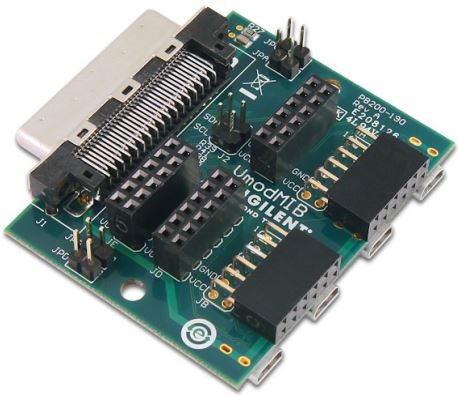
The Digilent Vmod Module Interface Board (VmodMIB) is a simple solution for interfacing additional peripheral modules and HDMI devices to VHDCI-equipped Digilent system boards.
Features include:
- VHDCI peripheral board connector
- Four HDMI and five 12-pin Pmod™ connectors
Functional Description
The VmodMIB is an expansion board that connects to the VHDCI connector on Digilent system boards and provides additional Pmod and HDMI connections.
Power Connections
The VmodMIB provides two power buses and a ground bus. The two power buses are labeled VCC and VU. These two buses are made available at each connector position on the board. There is also a ground plane that connects the ground pins from all connectors. The usual Digilent convention is to power the VCC bus at 3.3V and the VCCFX2 bus at 5.0V. However, depending on the system board connected and the power supply used, other voltages may be present. Use caution when using any voltage other than 3.3V on the VCC bus. Most Digilent system boards will be damaged if the voltage on the VCC bus is greater than 3.3V.
68 Pin, VHDCI Connector
VHDCI connector J1 is provided on one side of the board for connection to Digilent system boards, like the Genesys™ and Atlys™, which contain a VHDCI-style connector. The Digilent VHDCI connector signal convention provides for 40 general-purpose I/O signals. The 40 general-purpose I/O signals from the VHDCI connector are brought out to the Pmod and HDMI connectors. See Table 1 for a description of the relationship between the VHDCI connector pins and the signal names, Table 2 for the relationship between signal names and Pmod pins and Table 3 for the relationship between signal names and HDMI pins.
Pmod Connectors
Digilent Pmods provide various peripheral functions. These can be as simple as buttons or switches for inputs and LEDs for outputs, or as complex as graphical LCD display panels, accelerometers, and keypads. All Digilent Pmods use either a 6-wire interface or a 12-wire interface. The 6-wire interface provides four I/O signals, power, and ground. The twelve-wire interface provides 8 I/O signals, two powers, and two grounds. The signal definitions for the I/O signals as well as the voltage requirements for the power supply depend on the specific module. The VmodMIB provides five 12-pin Pmod connectors.
HDMI Connectors
The VmodMIB also provides four HDMI type-D connectors to allow audio/video connections to the system board. They use 19 pins and the relationship between these pins and the signal names from the VHDCI connector are described in table 3. Each HDMI connector has a jumper which can be used to select a 5V source when shorted. Also, data can be sent to the HDMI connectors via an I2C bus from signals JE1/SDA and JE2/SCL when the jumpers at J2 are shorted. Keep in mind that all HDMI ports share signals with Pmod ports. JA is shares signals with JAA, JB with JBB, JC with JCC, and JD with JDD. All HDMI ports share pins with Pmod port JE, which contains the I2C bus signals.
Table 1: VHDCI Signals and Connector Pinout
J1
| 1 | JC-CLK_P | 35 | JC-CLK_N |
| 2 | GND | 36 | GND |
| 3 | JC-D0_P | 37 | JC-D0_N |
| 4 | JC-D1_P | 38 | JC-D1_N |
| 5 | GND | 39 | GND |
| 6 | JC-D2_P | 40 | JC-D2_N |
| 7 | JA-D0_P | 41 | JA-D0_N |
| 8 | GND | 42 | GND |
| 9 | JA-D1_P | 43 | JA-D1_N |
| 10 | JA-D2_P | 44 | JA-D2_N |
| 11 | GND | 45 | GND |
| 12 | JB-D0_P | 46 | JB-D0_N |
| 13 | JB-D1_P | 47 | JB-D1_N |
| 14 | GND | 48 | GND |
| 15 | JA-CLK_P | 49 | JA-CLK_N |
| 16 | VCCB | 50 | VCCB |
| 17 | VCC5V0 | 51 | VCC5V0 |
| 18 | VCC5V0 | 52 | VCC5V0 |
| 19 | VCCB | 53 | VCCB |
| 20 | JB-CLK_P | 54 | JB-CLK_N |
| 21 | GND | 55 | GND |
| 22 | JB-D2_P | 56 | JB-D2_N |
| 23 | JE8 | 57 | JE7 |
| 24 | GND | 58 | GND |
| 25 | JE2/SCL | 59 | JE1/SDA |
| 26 | JE10 | 60 | JE9 |
| 27 | GND | 61 | GND |
| 28 | JE4 | 62 | JE3 |
| 29 | JD-CLK_P | 63 | JD-CLK_N |
| 30 | GND | 64 | GND |
| 31 | JD-D0_P | 65 | JD-D0_N |
| 32 | JD-D1_P | 66 | JD-D1_N |
| 33 | GND | 67 | GND |
| 34 | JD-D2_P | 68 | JD-D2_N |
| S1 | SHIELD | S2 | SHIELD |
Table 2: Pmod Connector Pin Layouts
JA Top Set of Pins
| Pin | Pinout |
| 1 | JA-D0_N |
| 2 | JA-D0_P |
| 3 | JA-D2_N |
| 4 | JA-D2_P |
| 5 | GND |
| 6 | VCCB |
JB Top Set of Pins
| Pin | Pinout |
| 1 | JB-D0_N |
| 2 | JB-D0_P |
| 3 | JB-D2_N |
| 4 | JB-D2_P |
| 5 | GND |
| 6 | VCCB |
JC Top Set of Pins
| Pin | Pinout |
| 1 | JC-D0_N |
| 2 | JC-D0_P |
| 3 | JC-D2_N |
| 4 | JC-D2_P |
| 5 | GND |
| 6 | VCCB |
JD Top Set of Pins
| Pin | Pinout |
| 1 | JD-D0_N |
| 2 | JD-D0_P |
| 3 | JD-D2_N |
| 4 | JD-D2_P |
| 5 | GND |
| 6 | VCCB |
JE Top Set of Pins
| Pin | Pinout |
| 1 | JE1/SDA |
| 2 | JE2/SCL |
| 3 | JE3 |
| 4 | JE4 |
| 5 | GND |
| 6 | VCCB |
NOTE: All signals are connected via a 50-ohm resistor with the exception of the VCCB and GND signals.
JA Bottom Set of Pins
| Pin | Pinout |
| 7 | JA-CLK_N |
| 8 | JA-CLK_P |
| 9 | JA-D1_N |
| 10 | JA-D1_P |
| 11 | GND |
| 12 | VCCB |
JB Bottom Set of Pins
| Pin | Pinout |
| 7 | JB-CLK_N |
| 8 | JB-CLK_P |
| 9 | JB-D1_N |
| 10 | JB-D1_P |
| 11 | GND |
| 12 | VCCB |
JC Bottom Set of Pins
| Pin | Pinout |
| 7 | JC-CLK_N |
| 8 | JC-CLK_P |
| 9 | JC-D1_N |
| 10 | JC-D1_P |
| 11 | GND |
| 12 | VCCB |
JD Bottom Set of Pins
| Pin | Pinout |
| 7 | JD-CLK_N |
| 8 | JD-CLK_P |
| 9 | JD-D1_N |
| 10 | JD-D1_P |
| 11 | GND |
| 12 | VCCB |
JE Bottom Set of Pins
| Pin | Pinout |
| 1 | JE7 |
| 2 | JE8 |
| 3 | JE9 |
| 4 | JE10 |
| 5 | GND |
| 6 | VCCB |
Table 3: HDMI Connector Pin Layouts
JAA
| Pin | Pinout |
| 1 | VCC5V0 |
| 2 | VCCB |
| 3 | JA-D2_P |
| 4 | GND |
| 5 | JA-D2_N |
| 6 | JA-D1_P |
| 7 | GND |
| 8 | JA-D1_N |
| 9 | JA-D0_P |
| 10 | GND |
| 11 | JA-D0_N |
| 12 | JA-CLK_P |
| 13 | GND |
| 14 | JA-CLK_N |
| 15 | VCCB |
| 16 | GND |
| 17 | JE2/SCL |
| 18 | JE1/SDA |
| 19 | VCC5V0 |
JBB
| Pin | Pinout |
| 1 | VCC5V0 |
| 2 | VCCB |
| 3 | JB-D2_P |
| 4 | GND |
| 5 | JB-D2_N |
| 6 | JB-D1_P |
| 7 | GND |
| 8 | JB-D1_N |
| 9 | JB-D0_P |
| 10 | GND |
| 11 | JB-D0_N |
| 12 | JB-CLK_P |
| 13 | GND |
| 14 | JB-CLK_N |
| 15 | VCCB |
| 16 | GND |
| 17 | JE2/SCL |
| 18 | JE1/SDA |
| 19 | VCC5V0 |
JCC
| Pin | Pinout |
| 1 | VCC5V0 |
| 2 | VCCB |
| 3 | JC-D2_P |
| 4 | GND |
| 5 | JC-D2_N |
| 6 | JC-D1_P |
| 7 | GND |
| 8 | JC-D1_N |
| 9 | JC-D0_P |
| 10 | GND |
| 11 | JC-D0_N |
| 12 | JC-CLK_P |
| 13 | GND |
| 14 | JC-CLK_N |
| 15 | VCCB |
| 16 | GND |
| 17 | JE2/SCL |
| 18 | JE1/SDA |
| 19 | VCC5V0 |
JDD
| Pin | Pinout |
| 1 | VCC5V0 |
| 2 | VCCB |
| 3 | JD-D2_P |
| 4 | GND |
| 5 | JD-D2_N |
| 6 | JD-D1_P |
| 7 | GND |
| 8 | JD-D1_N |
| 9 | JD-D0_P |
| 10 | GND |
| 11 | JD-D0_N |
| 12 | JD-CLK_P |
| 13 | GND |
| 14 | JD-CLK_N |
| 15 | VCCB |
| 16 | GND |
| 17 | JE2/SCL |
| 18 | JE1/SDA |
| 19 | VCC5V0 |
NOTE: All signals are connected via a 50-ohm resistor
Copyright Digilent, Inc. All rights reserved. Other product and company names mentioned may be trademarks of their respective owners.
Documents / Resources
 |
DIGILENT VmodMIB Digilent Vmod Module Interface Board [pdf] Owner's Manual VmodMIB Digilent Vmod Module Interface Board, VmodMIB, Digilent Vmod Module Interface Board, Interface Board, Board |