![]() FPGA IP
FPGA IP
Design Example User Guide
F-Tile 25G Ethernet Intel®
Updated for Intel® Quartus®
Prime Design Suite: 22.3
IP Version: 1.0.0
Quick Start Guide
The F-tile 25G Ethernet Intel FPGA IP for Intel Agilex™ devices provides the capability of generating design examples for selected configurations.
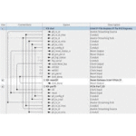
Figure 1. Design Example Usage

Directory Structure
Figure 2. 25G Ethernet Intel FPGA IP Design Example Directory Structure

- The simulation files (testbench for simulation only) are located in <design_example_dir>/example_testbench.
- The compilation-only design example is located in <design_example_dir>/ compilation_test_design.
- The hardware configuration and test files (the design example in hardware) are located in <design_example_dir>/hardware_test_design.
Table 1. Directory and File Descriptions
| File Names | Description |
| eth_ex_25g.qpf | Intel Quartus® Prime project file. |
| eth_ex_25g.qsf | Intel Quartus Prime project settings file. |
| eth_ex_25g.sdc | Synopsys Design Constraints file. You can copy and modify this file for your own 25GbE Intel FPGA IP core design. |
| eth_ex_25g.v | Top-level Verilog HDL design example file. Single-channel design uses Verilog file. |
| common/ | Hardware design example support files. |
| hwtest/main.tcl | Main file for accessing System Console. |
Generating the Design Example

Figure 4. Example Design Tab in the F-tile 25G Ethernet Intel FPGA IP Parameter Editor

Follow these steps to generate the hardware design example and testbench:
- In the Intel Quartus Prime Pro Edition, click File ➤ New Project Wizard to create a new Quartus Prime project, or File ➤ Open Project to open an existing Quartus Prime project. The wizard prompts you to specify a device.
- In the IP Catalog, locate and select 25G Ethernet Intel FPGA IP for Agilex. The New IP Variation window appears.
- Specify a top-level name for your IP variation and click OK. The parameter editor adds the top-level .ip file to the current project automatically. If you are prompted to manually add the .ip file to the project, click Project ➤ Add/ Remove Files in Project to add the file.
- In the Intel Quartus Prime Pro Edition software, you must select a specific Intel Agilex device in the Device field, or keep the default device the Intel Quartus Prime software proposes.
Note: The hardware design example overwrites the selection with the device on the target board. You specify the target board from the menu of design example options in the Example Design tab. - Click OK. The parameter editor appears.
- On the IP tab, specify the parameters for your IP core variation.
- On the Example Design tab, for Example Design Files, select the Simulation option to generate the testbench, and select the Synthesis option to generate the hardware design example. Only Verilog HDL files are generated.
Note: A functional VHDL IP core is not available. Specify Verilog HDL only, for your IP core design example. - For Target Development Kit, select the Agilex I-series Transceiver-SoC Dev Kit
- Click the Generate Example Design button. The Select Example Design Directory window appears.
- If you wish to modify the design example directory path or name from the defaults displayed (alt_e25_f_0_example_design), browse to the new path and type the new design example directory name (<design_example_dir>).
- Click OK.
1.2.1. Design Example Parameters
Table 2. Parameters in the Example Design Tab
| Parameter | Description |
| Example Design | Available example designs for the IP parameter settings. Only single- channel example design is supported for this IP. |
| Example Design Files | The files to generate for the different development phase. • Simulation—generates the necessary files for simulating the example design. • Synthesis—generates the synthesis files. Use these files to compile the design in the Intel Quartus Prime Pro Edition software for hardware testing and perform static timing analysis. |
| Generate File Format | The format of the RTL files for simulation—Verilog. |
| Select Board | Supported hardware for design implementation. When you select an Intel FPGA development board, use device AGIB027R31B1E2VRO as the Target Device for design example generation. Agilex I-series Transceiver-SoC Dev Kit: This option allows you to test the design example on the selected Intel FPGA IP development kit. This option automatically selects the Target Device of AGIB027R31B1E2VRO. If your board revision has a different device grade, you can change the target device. None: This option excludes the hardware aspects for the design example. |
1.3. Generating Tile Files
The Support-Logic Generation is a pre-synthesis step used to generate tile-related files required for simulation and hardware design. The tile generation is required for all
F-tile based design simulations. You must complete this step before the simulation.
- At the command prompt, navigate to the compilation_test_design folder in your example design: cd <your_design_path>/compilation_test_design.
- Run the following command: quartus_tlg alt_eth_25g
1.4. Simulating the F-tile 25G Ethernet Intel FPGA IP Design
Example Testbench
You can compile and simulate the design by running a simulation script from the command prompt.

- At the command prompt, change the testbench simulating working directory: cd <design_example_dir>/ex_25g/sim.
- Run the IP setup simulation:ip-setup-simulation -quartusproject=../../compilation_test_design/alt_eth_25g.qpf
Table 3. Steps to Simulate the Testbench
| Simulator | Instructions |
| VCS* | In the command line, type sh run_vcs.sh |
| QuestaSim* | In the command line, type vsim -do run_vsim.do -logfile vsim.log If you prefer to simulate without bringing up the QuestaSim GUI, type vsim -c -do run_vsim.do -logfile vsim.log |
| Cadence -Xcelium* | In the command line, type sh run_xcelium.sh |
A successful simulation ends with the following message:
Simulation Passed. or Testbench complete.
After successful completion, you can analyze the results.
1.5. Compiling and Configuring the Design Example in Hardware
The 25G Ethernet Intel FPGA IP core parameter editor allows you to compile and configure the design example on a target development kit.

To compile and configure a design example on hardware, follow these steps:
- Launch the Intel Quartus Prime Pro Edition software and select Processing ➤ Start Compilation to compile the design.
- After you generate an SRAM object file .sof, follow these steps to program the hardware design example on the Intel Agilex device:
a. On the Tools menu, click Programmer.
b. In the Programmer, click Hardware Setup.
c. Select a programming device.
d. Select and add the Intel Agilex board to your Intel Quartus Prime Pro Edition session.
e. Ensure that Mode is set to JTAG.
f. Select the Intel Agilex device and click Add Device. The Programmer displays
a block diagram of the connections between the devices on your board.
g. In the row with your .sof, check the box for the .sof.
h. Check the box in the Program/Configure column.
i. Click Start.
1.6. Testing the F-tile 25G Ethernet Intel FPGA IP Hardware Design Example
After you compile the F-tile 25G Ethernet Intel FPGA IP core design example and configure it on your Intel Agilex device, you can use the System Console to program the IP core.
To turn on the System Console and test the hardware design example, follow these steps:
- In the Intel Quartus Prime Pro Edition software, select Tools ➤ System
Debugging Tools ➤ System Console to launch the system console. - In the Tcl Console pane, type cd hwtest to change directory to / hardware_test_design/hwtest.
- Type source main.tcl to open a connection to the JTAG master.
Follow the test procedure in the Hardware Testing section of the design example and observe the test results in the System Console.
F-tile 25G Ethernet Design Example for Intel Agilex Devices
The F-tile 25G Ethernet design example demonstrates an Ethernet solution for Intel Agilex devices using the 25G Ethernet Intel FPGA IP core.
Generate the design example from the Example Design tab of the 25G Ethernet Intel FPGA IP parameter editor. You can also choose to generate the design with or without
the Reed-Solomon Forward Error Correction (RS-FEC) feature.
2.1. Features
- Supports single Ethernet channel operating at 25G.
- Generates design example with RS-FEC feature.
- Provides testbench and simulation script.
- Instantiates F-Tile Reference and System PLL Clocks Intel FPGA IP based on IP configuration.
2.2. Hardware and Software Requirements
Intel uses the following hardware and software to test the design example in a Linux system:
- Intel Quartus Prime Pro Edition software.
- Siemens* EDA QuestaSim, Synopsys* VCS, and Cadence Xcelium simulator.
- Intel Agilex I-series Transceiver-SoC Development Kit (AGIB027R31B1E2VRO) for hardware testing.
2.3. Functional Description
The F-tile 25G Ethernet design example consists of MAC+PCS+PMA core variant. The following block diagrams show the design components and the top-level signals of the MAC+PCS+PMA core variant in the F-tile 25G Ethernet design example.
Figure 5. Block Diagram—F-tile 25G Ethernet Design Example (MAC+PCS+PMA Core Variant)

2.3.1. Design Components
Table 4. Design Components
| Component | Description |
| F-tile 25G Ethernet Intel FPGA IP | Consists of MAC, PCS, and Transceiver PHY, with the following configuration: • Core Variant: MAC+PCS+PMA • Enable flow control: Optional • Enable link fault generation: Optional • Enable preamble passthrough: Optional • Enable statistics collection: Optional • Enable MAC statistics counters: Optional • Reference clock frequency: 156.25 For the design example with the RS-FEC feature, the following additional parameter is configured: • Enable RS-FEC: Optional |
| F-Tile Reference and System PLL Clocks Intel FPGA IP | The F-Tile Reference and System PLL Clocks Intel FPGA IP parameter editor settings align with the requirements of the F-tile 25G Ethernet Intel FPGA IP. If you generate the design example using Generate Example Design button in the IP parameter editor, the IP instantiates automatically. If you create your own design example, you must manually instantiate this IP and connect all I/O ports. For information about this IP, refer to F-Tile Architecture and PMA and FEC Direct PHY IP User Guide. |
| Client logic | Consists of: • Traffic generator, which generates burst packets to the 25G Ethernet Intel FPGA IP core for transmission. • Traffic monitor, which monitors burst packets that are coming from the 25G Ethernet Intel FPGA IP core. |
| Source and Probe | Source and probe signals, including system reset input signal, which you can use for debugging. |
Related Information
F-Tile Architecture and PMA and FEC Direct PHY IP User Guide
Simulation
The testbench sends traffic through the IP core, exercising the transmit side and receive side of the IP core.
2.4.1. Testbench
Figure 6. Block Diagram of the F-tile 25G Ethernet Intel FPGA IP Design Example Simulation Testbench

Table 5. Testbench Components
| Component | Description |
| Device under test (DUT) | The 25G Ethernet Intel FPGA IP core. |
| Ethernet Packet Generator and Packet Monitor | • Packet generator generates frames and transmit to the DUT. • Packet Monitor monitors TX and RX datapaths and displays the frames in the simulator console. |
| F-Tile Reference and System PLL Clocks Intel FPGA IP | Generates transceiver and system PLL reference clocks. |
2.4.2. Simulation Design Example Components
Table 6. F-tile 25G Ethernet Design Example Testbench File Descriptions
| File Name | Description |
| Testbench and Simulation Files | |
| basic_avl_tb_top.v | Top-level testbench file. The testbench instantiates the DUT, performs Avalon® memory-mapped configuration on design components and client logic, and sends and receives packet to or from the 25G Ethernet Intel FPGA IP. |
| Testbench Scripts | |
| continued… | |
| File Name | Description |
| run_vsim.do | The ModelSim script to run the testbench. |
| run_vcs.sh | The Synopsys VCS script to run the testbench. |
| run_xcelium.sh | The Cadence Xcelium script to run the testbench. |
2.4.3. Test Case
The simulation test case performs the following actions:
- Instantiates F-tile 25G Ethernet Intel FPGA IP and F-Tile Reference and System PLL Clocks Intel FPGA IP.
- Waits for RX clock and PHY status signal to settle.
- Prints PHY status.
- Sends and receives 10 valid data.
- Analyzes the results. The successful testbench displays “Testbench complete.”.
The following sample output illustrates a successful simulation test run:

Compilation
Follow the procedure in Compiling and Configuring the Design Example in Hardware to compile and configure the design example in the selected hardware.
You can estimate resource utilization and Fmax using the compilation-only design example. You can compile your design using the Start Compilation command on the
Processing menu in the Intel Quartus Prime Pro Edition software. A successful compilation generates the compilation report summary.
For more information, refer to Design Compilation in the Intel Quartus Prime Pro Edition User Guide.
Related Information
- Compiling and Configuring the Design Example in Hardware on page 7
- Design Compilation In Intel Quartus Prime Pro Edition User Guide
2.6. Hardware Testing
In the hardware design example, you can program the IP core in internal serial loopback mode and generate traffic on the transmit side that loops back through the receive side.
Follow the procedure at the provided related information link to test the design example in the selected hardware.
Related Information
Testing the F-tile 25G Ethernet Intel FPGA IP Hardware Design Example on page 8
2.6.1. Test Procedure
Follow these steps to test the design example in hardware:
- Before you run the hardware testing for this design example, you must reset the system:
a. Click Tools ➤ In-System Sources & Probes Editor tool for the default Source and Probe GUI.
b. Toggle the system reset signal (Source[3:0]) from 7 to 8 to apply the resets and return the system reset signal back to 7 to release the system from the reset state.
c. Monitor the Probe signals and ensure that the status is valid. - In the system console, navigate to the hwtest folder and run the command: source main.tcl to select a JTAG master. By default, the first JTAG master on the JTAG chain is selected. To select the JTAG master for Intel Agilex devices, run this command: set_jtag <number of appropriate JTAG master>. Example: set_jtag 1.
- Run the following commands in the system console to start the serial loopback test:
Table 7. Command Parameters
| Parameter | Description | Example Usage |
| chkphy_status <link num> | Displays the clock frequencies and PHY lock status. | % chkphy_status 0 # Check status of link 0 |
| chkmac_stats <link num> | Displays the values in the MAC statistics counters. | % chkmac_stats 0 # Checks mac statistics counter of link 0 |
| clear_all_stats <link num> | Clears the IP core statistics counters. | % clear_all_stats 0 # Clears statistics counter of link 0 |
| start_gen <link num> | Starts the packet generator. | % start_gen 0 # Begin packet generation on link 0 |
| stop_gen <link num> | Stops the packet generator. | % stop_gen 0 # Stop packet generation on link 0 |
| loop_on <link num> | Turns on internal serial loopback. | % loop_on 0 # Turn on internal loopback on link 0 |
| loop_off <link num> | Turns off internal serial loopback. | % loop_off 0 # Turn off internal loopback on link 0 |
| reg_read <addr> | Returns the IP core register value at <addr>. | % reg_read 0x402 # Read IP CSR register at address 402 of link 0 |
| reg_write <addr> <data> | Writes <data> to the IP core register at address <addr>. | % reg_write 0x401 0x1 # Write 0x1 to IP CSR scratch register at address 401 of link 0 |
a. Type loop_on <link num> to turn on the internal serial loopback mode.
b. Type chkphy_status <link num> to check the status of the PHY. The TXCLK, RXCLK, and RX status should have the same values shown below for a stable link:

c. Type clear_all_stats <link num> to clear TX and RX statistics registers.
d. Type start_gen <link num> to begin packet generation.
e. Type stop_gen <link num> to stop packet generation.
f. Type chkmac_stats <link num> to read the TX and RX statistics counters. Make sure that:
i. The transmitted packet frames match the received packet frames.
ii. No error frames are received.
g. Type loop_off <link num> to turn off the internal serial loopback.
Figure 7. Sample Test Output—TX and RX Statistics Counters
 |
 |
Document Revision History for F-tile 25G Ethernet FPGA IP Design Example User Guide
| Document Version | Intel Quartus Prime Version | IP Version | Changes |
| 2022.10.14 | 22.3 | 1.0.0 | Initial release. |
Intel Corporation. All rights reserved. Intel, the Intel logo, and other Intel marks are trademarks of Intel Corporation or its subsidiaries. Intel warrants performance of its FPGA and semiconductor products to current specifications in accordance with Intel’s standard warranty, but reserves the right to make changes to any products and services at any time without notice. Intel assumes no responsibility or liability arising out of the application or use of any information, product, or service described herein except as expressly agreed to in writing by Intel. Intel customers are advised to obtain the latest version of device specifications before relying on any published information and before placing orders for products or services. *Other names and brands may be claimed as the property of others.
ISO
9001:2015
Registered
![]()
 Online Version
![]() Send Feedback
Send Feedback
ID: 750200
Version: 2022.10.14
Documents / Resources
 |
intel F-Tile 25G Ethernet FPGA IP Design Example [pdf] User Guide F-Tile 25G Ethernet FPGA IP Design Example, F-Tile 25G, F-Tile 25G Ethernet FPGA, FPGA IP Design Example, IP Design Example, 750200 |