Handson Technology DSP-1165 I2C Serial Interface 20×4 LCD Module

Specifications
- Compatible with Arduino Board or other controller board with I2C bus.
- Display Type: Black on yellow-green backlight.
- I2C Address: 0x38-0x3F (0x3F default).
- Supply voltage: 5V.
- Interface: I2C to 4-bit LCD data and control lines.
- Contrast Adjustment: built-in Potentiometer.
- Backlight Control: Firmware or jumper wire.
- Board Size: 98×60 mm.
Product Usage Instructions
Setting Up
Address selection pads in the I2C-to-LCD piggyback board. The default address setting is 3Fh. Follow the reference circuit diagram to interface with a microcontroller.
I2C LCD Display Setup
- Solder the I2C-to-LCD piggy-back board to the 16-pin LCD module ensuring proper alignment.
- Connect the LCD module to your Arduino using four jumper wires as per the instruction manual.
Arduino Setup:
- Download and install the Arduino I2C LCD library. Rename the existing LiquidCrystal library folder in your Arduino libraries folder as a backup.
- Copy and paste the provided example sketch into the Arduino IDE, verify, and upload the sketch to your Arduino board.
FAQ:
Q: What is the default I2C address of the module?
- A: The default I2C address is 0x3F, but it can be set between 0x38-0x3F.
Q: How do I adjust the contrast of the display?
- A: The module has a built-in potentiometer for contrast adjustment.
Q: Can I control the backlight of the display?
- A: Yes, you can control the backlight either through firmware or by using a jumper wire.
- This is an I2C interface 20×4 LCD module, a new high-quality 4-line 20-character LCD module with on-board contrast control adjustment, backlight, and I2C communication interface.
- For Arduino beginners, no more cumbersome and complex LCD driver circuit connection.
- The real significant advantages of this I2C Serial LCD module will simplify the circuit connection, save some I/O pins on the Arduino board, simplified firmware development with a widely available Arduino library.
- SKU: DSP-1165
Brief Data:
- Compatible with Arduino Board or other controller board with I2C bus.
- Display Type: Black on yellow-green backlight.
- I2C Address:0x38-0x3F (0x3F default)
- Supply voltage: 5V
- Interface: I2C to 4-bit LCD data and control lines.
- Contrast Adjustment: built-in Potentiometer.
- Backlight Control: Firmware or jumper wire.
- Board Size: 98×60 mm.
Setting Up
- Hitachi’s HD44780-based character LCD is very cheap and widely available and is an essential part of any project that displays information.
- Using the LCD piggyback board, desired data can be displayed on the LCD through the I2C bus. In principle, such backpacks are built around PCF8574 (from NXP) which is a general-purpose bidirectional 8-bit I/O port expander that uses the I2C protocol.
- The PCF8574 is a silicon CMOS circuit that provides general-purpose remote I/O expansion (an 8-bit quasi-bidirectional) for most microcontroller families via the two-line bidirectional bus (I2C-bus).
- Note that most piggy-back modules are centered around PCF8574T (SO16 package of PCF8574 in DIP16 package) with a default slave address of 0x27.
- If your piggyback board holds a PCF8574AT chip, then the default slave address will change to 0x3F.
- In short, if the piggyback board is based on PCF8574T and the address connections (A0-A1-A2) are not bridged with solder it will have the slave address 0x27.

Address Setting of PCD8574A (extract from PCF8574A data specs)
- Note: When the pad A0~A2 is open, the pin is pulled up to VDD. When the pin is solder shorted, it is pulled down to VSS.
- The default setting of this module is A0~A2 all open, so is pulled up to VDD. The address is 3Fh in this case.
- A reference circuit diagram of an Arduino-compatible LCD backpack is shown below.
- What follows next is information on how to use one of these inexpensive backpacks to interface with a microcontroller in ways it was exactly intended.

- Reference circuit diagram of the I2C-to-LCD piggyback board.
I2C LCD Display.
- First, you need to solder the I2C-to-LCD piggyback board to the 16-pin LCD module. Ensure that the I2C-to-LCD piggy-back board pins are straight and fit in the LCD module, then solder in the first pin while keeping the I2C-to-LCD piggy-back board in the same plane as the LCD module. Once you have finished the soldering work, get four jumper wires and connect the LCD module to your Arduino as per the instructions given below.

- LCD to Arduino wiring

Arduino Setup
- For this experiment, it is necessary to download and install the “Arduino I2C LCD” library.
- First of all, rename the existing “LiquidCrystal” library folder in your Arduino libraries folder as a backup, and proceed to the rest of the process.
- https://bitbucket.org/fmalpartida/new-liquidcrystal/downloads
- Next, copy-paste this example sketch Listing-1 for the experiment into the blank code window, verify, and then upload.
Arduino Sketch Listing-1:

- If you are 100% sure that everything is okay, but you don’t see any characters on the display, try to adjust the contrast control pot of the backpack and set it in a position where the characters are bright and the background does not have dirty boxes behind the characters. Following is a partial view of the author’s experiment with the above-described code with a 20×4 display module.
- Since the display used by the author is a very clear bright “black on yellow” type, it is very difficult to get a good catch due to polarization effects.
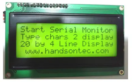
This sketch will also display the character sent from the serial Monitor:
- In Arduino IDE, go to “Tools” > “Serial Monitor”. Set the correct baud rate at 9600.
- Type the character on the top space and hit “SEND”.
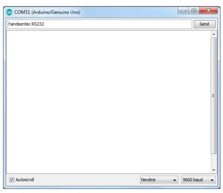
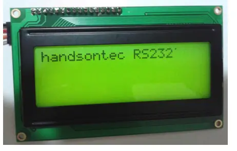
- The string of characters will be displayed on the LCD module.
Resources
- Handson Technology
- Lelong.com.my
- HandsOn Technology provides a multimedia and interactive platform for everyone interested in electronics.
- From beginner to diehard, from student to lecturer. Information, education, inspiration, and entertainment.
- Analog and digital, practical and theoretical; software and hardware.
- HandsOn Technology supports the Open Source Hardware (OSHW) Development Platform.
- Learn: Design Share www.handsontec.com
The Face behind our product quality
- In a world of constant change and continuous technological development, a new or replacement product is never far away – and they all need to be tested.
- Many vendors simply import and sell without checks and this cannot be the ultimate interest of anyone, particularly the customer. Every part sold on Handsotec is fully tested.
- So when buying from Handsontec products range, you can be confident you’re getting outstanding quality and value.
- We keep adding the new parts so that you can get rolling on your next project.

Features
- 5×8 dots with cursor
- STN(Yellow-Green), Positive, Transflective
- 1/16 duty cycle
- Viewing direction: 6:00 o’clock
- Built-in controller (S6A0069 or equivalent)
- +5V power supply
- Yellow-Green LED BKL, to be driven by A, K
Outline dimension

Absolute maximum ratings
| Item | Symbol | Standard | Unit | ||
| Power voltage | VDD-VSS | 0 | – | 7.0 | V |
| Input voltage | Vin | VSS | – | VDD | |
| Operating temperature range | Top | -20 | – | +70 | ℃ |
| Storage temperature range | Test | -30 | – | +80 | |
Block diagram

Interface pin description
| Pin no. | Symbol | External connection | Function |
| 1 | VSS | Power supply | Signal ground for LCM (GND) |
| 2 | VDD | Power supply for logic (+5V) for LCM | |
| 3 | V0 | Contrast adjust | |
| 4 | RS | MPU | Register select signal |
| 5 | R/W | MPU | Read/write select signal |
| 6 | E | MPU | Operation (data read/write) enable signal |
| 7~10 | DB0~DB3 | MPU | Four low-order bi-directional three-state data bus lines. Used for data transfer between the MPU and the LCM.
These four are not used during 4-bit operation. |
| 11~14 | DB4~DB7 | MPU | Four high-order bi-directional three-state data bus lines. Used for data transfer between the MPU |
| 15 | A(LED+) | LED BKL Power Supply | Power supply for BKL(Anode) |
| 16 | K(LED-) | Power supply for BKL (GND) |
Contrast adjust
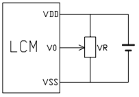
- VDD~V0: LCD Driving Voltage
- VR: 10k~20k
Optical characteristics

| Item | Symbol | Condition | Min. | Typ. | Max. | Unit |
| Viewing angle | θ1 | Cr≥3 | 20 | deg | ||
| θ2 | 40 | |||||
| Φ1 | 35 | |||||
| Φ2 | 35 | |||||
| Contrast ratio | Cr | – | 10 | – | – | |
| Response time (rise) | Tr | – | – | 200 | 250 | ms |
| Response time (fall) | Tr | – | – | 300 | 350 |
Electrical characteristics
Backlight circuit diagram(light 12X4)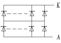
COLOUR: YELLOW-GREEN
LED RATINGS
| ITEM | SYMBOL | MIN | TYP. | MAX | UNIT |
| FORWARD VOLTAGE | VF | 4.0 | 4.2 | 4.4 | V |
| FORWARD CURRENT | IF | – | 240 | – | MA |
| POWER | P | – | 1.0 | – | W |
| PEAK WAVELENGTH | ΛP | 569 | 571 | 573 | NM |
| LUMINANCE | LV | – | 340 | – | CD/M2 |
| Operating temperature range | Vop | -20 | – | +70 | ℃ |
| Storage temperature range | Vst | -25 | – | +80 |
DC characteristics
| Parameter | Symbol | Conditions | Min. | Typ. | Max. | Unit |
| Supply voltage for LCD | VDD-V0 | Ta =25℃ | – | 4.5 | – | V |
| Input voltage | VDD | 4.7 | 5.0 | 5.5 | ||
| Supply current | ADD | Ta=25℃, VDD=5.0V | – | 1.5 | 2.5 | mA |
| Input leakage current | ILKG | – | – | 1.0 | uA | |
| “H” level input voltage | VIA | 2.2 | – | VDD | V | |
| “L” level input voltage | VIL | Twice the initial value or less | 0 | – | 0.6 | |
| “H” level output voltage | VOH | LOH=-0.25mA | 2.4 | – | – |
| “L” level output voltage | VOL | LOH=1.6mA | – | – | 0.4 | |
| Backlight supply current | IF | VDD=5.0V,R=6.8W | – | 240 | – |
Write cycle (Ta=25℃, VDD=5.0V)
| Parameter | Symbol | Test pin | Min. | Typ. | Max. | Unit |
| Enable cycle time | tc |
E |
500 | – | – |
ns |
| Enable pulse width | tw | 230 | – | – | ||
| Enable rise/fall time | tr, tf | – | – | 20 | ||
| RS; R/W setup time | tsu1 | RS; R/W | 40 | – | – | |
| RS; R/W address hold time | th1 | 10 | – | – | ||
| Data output delay | tsu2 | DB0~DB7 | 80 | – | – | |
| Data hold time | th2 | 10 | – | – |
Write mode timing diagram

Read cycle (Ta=25℃, VDD=5.0V)
| Parameter | Symbol | Test pin | Min. | Typ. | Max. | Unit |
| Enable cycle time | to | E | 500 | – | – | ns |
| Enable pulse width | TW | 230 | – | – | ||
| Enable rise/fall time | tr, tf | – | – | 20 | ||
| RS; R/W setup time | tsu | RS; R/W | 40 | – | – | |
| RS; R/W address hold time | th | 10 | – | – | ||
| Data output delay | td | DB0~DB7 | – | – | 120 | |
| Data hold time | the | 5 | – | – |
Read mode timing diagram
FUNCTION DESCRIPTION
System Interface
- This chip has two kinds of interface types with MPU: 4-bit bus and 8-bit bus. 4-bit bus and 8-bit bus are selected by DL bit in the instruction register.
Busy Flag (BF)
- When BF = “High”, it indicates that the internal operation is being processed. So during this time, the next instruction cannot be accepted.
- BF can be read, when RS = Low and R/W = High (Read Instruction Operation), through the DB7 port. Before executing the next instruction, be sure that BF is not high.
Address Counter (AC)
- Address Counter (AC) stores DDRAM/CGRAM address, transferred from IR. After writing into (reading from) DDRAM/CGRAM, AC is automatically increased (decreased) by 1.
- When RS = “Low” and R/W = “High”, AC can be read through DB0 – DB6 ports.
Display Data RAM (DDRAM)
- DDRAM stores display data of a maximum of 80 x 8 bits (80 characters). DDRAM address is set in the address counter (AC) as a hexadecimal number.
Display position
| 1 | 2 | 3 | 4 | 5 | 6 | 7 | 8 | 9 | 10 | 11 | 12 | 13 | 14 | 15 | 16 | 17 | 18 | 19 | 20 |
| 00 | 01 | 02 | 03 | 04 | 05 | 06 | 07 | 08 | 09 | 0A | 0B | 0C | 0D | 0E | 0F | 10 | 11 | 12 | 13 |
| 40 | 41 | 42 | 43 | 44 | 45 | 46 | 47 | 48 | 49 | 4A | 4B | 4C | 4D | 4E | 4F | 50 | 51 | 52 | 53 |
| 14 | 15 | 16 | 17 | 18 | 19 | 1A | 1B | 1C | 1D | 1E | 1F | 20 | 21 | 22 | 23 | 24 | 25 | 26 | 27 |
| 54 | 55 | 56 | 57 | 58 | 59 | 5A | 5B | 5C | 5D | 5E | 5F | 60 | 61 | 62 | 63 | 64 | 65 | 66 | 67 |
CGROM (Character Generator ROM)
- CGROM has a 5 x 8 dots 204 characters pattern and a 5 x 10 dots 32 characters pattern. CGROM has 204 character patterns of 5 x 8 dots.
CGRAM (Character Generator RAM)
- CGRAM has up to 5 × 8 dots, 8 characters. By writing font data to CGRAM, user-defined characters can be used.

Relationship between CGRAM Addresses, Character Codes (DDRAM), and Character patterns (CGRAM Data)
Notes:
- Character code bits 0 to 2 correspond to CGRAM address bits 3 to 5 (3 bits: 8 types).
- CGRAM addresses bits 0 to 2 and designates the character pattern line position. The 8th line is the cursor position and its display is formed by a logical OR with the cursor. Maintain the 8th line data, corresponding to the cursor display position, at 0 as the cursor display. If the 8th line data is 1, 1 bit will light up the 8th line regardless of the cursor’s presence.
- Character pattern row positions correspond to CGRAM data bits 0 to 4 (bit 4 being at the left).
- As shown in Table, CGRAM character patterns are selected when character code bits 4 to 7 are all 0. However, since character code bit 3 has no effect, the R display example above can be selected by either character code 00H or 08H.
- 1 for CGRAM data corresponds to display selection and 0 for non-selection Indicates no effect.
Cursor/Blink Control Circuit
It controls the cursor/blink ON/OFF at the cursor position.
Instruction Description
Outline
- To overcome the speed difference between the internal clock of S6A0069 and the MPU clock, S6A0069 performs internal operations by storing control in formations to IR or DR.
- The internal operation is determined according to the signal from MPU, composed of read/write and data bus (Refer to Table 7).
Instructions can be divided largely into four groups:
- S6A0069 function set instructions (set display methods, set data length, etc.)
- Address set instructions to internal RAM
- Data transfer instructions with internal RAM
- Others
- The address of the internal RAM is automatically increased or decreased by 1.
- Note: during internal operation, busy flag (DB7) is read “High”.
- Busy flag check must be preceded by the next instruction.
Instruction Table
| Instruction
V: B |
Instruction code
6/18 |
Description
2008/06/02 |
Execution |
| RS | R/W | DB7 | DB6 | DB 5 | DB4 | DB3 | DB2 | DB 1 | DB0 | time (fosc= 270 KHZ | ||
| Clear Display | 0 | 0 | 0 | 0 | 0 | 0 | 0 | 0 | 0 | 1 | Write “20H” to DDRA and set the DDRAM address to “00H” from
AC |
1.53ms |
| Return Home |
0 |
0 |
0 |
0 |
0 |
0 |
0 |
0 |
1 |
– |
Set DDRAM address to “00H” From AC and return the cursor to Its original position if shifted.
The contents of DDRAM are not changed. |
1.53ms |
| Entry mode Set | 0 | 0 | 0 | 0 | 0 | 0 | 0 | 1 | I/D | SH | Assign cursor moving direction And blinking of the entire display | 39us |
| Display ON/ OFF control | 0 | 0 | 0 | 0 | 0 | 0 | 1 | D | C | B | Set display (D), cursor (C), and Blinking of cursor (B) on/off
Control bit. |
|
| Cursor or Display shift |
0 |
0 |
0 |
0 |
0 |
1 |
S/C |
R/L |
– |
– |
Set cursor moving and display Shift control bit, and the Direction, without changing of
DDRAM data. |
39us |
|
Function set |
0 |
0 |
0 |
0 |
1 |
DL |
N |
F |
– |
– |
Set interface data length (DL: 8-
Bit/4-bit), numbers of display Line (N: =2-line/1-line), and, Display font type (F: 5×11/5×8) |
39us |
| Set CGRAM
Address |
0 |
0 |
0 |
1 |
AC5 |
AC4 |
AC3 |
AC2 |
AC1 |
AC0 |
Set the CGRAM address in the address
Counter. |
39us |
| Set DDRAM
Address |
0 |
0 |
1 |
AC6 |
AC5 |
AC4 |
AC3 |
AC2 |
AC1 |
AC0 |
Set DDRAM address in the address
Counter. |
39us |
| Read busy Flag and Address |
0 |
1 |
BF |
AC6 |
AC5 |
AC4 |
AC3 |
AC2 |
AC1 |
AC0 |
Whether during internal Operation or not can be known By reading BF. The contents of the Address counter can also be read. |
0us |
| Write data to
Address |
1 |
0 |
D7 |
D6 |
D5 |
D4 |
D3 |
D2 |
D1 |
D0 |
Write data into internal RAM (DDRAM/CGRAM). |
43us |
| Read data From RAM | 1 | 1 | D7 | D6 | D5 | D4 | D3 | D2 | D1 | D0 | Read data from internal RAM (DDRAM/CGRAM). | 43us |
- NOTE: When an MPU program checking the busy flag (DB7) is made, it must be necessary 1/2fosc is necessary for executing the next instruction by the falling edge of the “E” signal after the busy flag (DB7) goes to “Low”.
Contents
- Clear display
RS R/W DB7 DB6 DB5 DB4 DB3 DB2 DB1 DB0 0 0 0 0 0 0 0 0 0 1 - Clear all the display data by writing “20H” (space code) to all DDRAM addresses, and set the DDRAM address to “00H” into AC (address counter).
- Return the cursor to the original status, namely, bring the cursor to the left edge on the first line of the display. Make the entry mode increment (I/D=“High”).
- Return home
RS R/W DB7 DB6 DB5 DB4 DB3 DB2 DB1 DB0 0 0 0 0 0 0 0 0 1 – - Return home is the cursor return home instruction.
- Set the DDRAM address to “00H” on the address counter.
- Return cursor to its original site and return the display to its original status, if shifted. The contents of DDRAM do not change.
- Entry mode set
RS R/W DB7 DB6 DB5 DB4 DB3 DB2 DB1 DB0 0 0 0 0 0 0 0 1 I/D SH - Set the moving direction of the cursor and display.
- I/D: increment/decrement of DDRAM address (cursor or blink)
- When I/D=“high”, the cursor/blink moves to the right, and the DDRAM address is increased by 1.
- When I/D=“Low”, the cursor/blink moves to the left and DDRAM address is increased by 1.
- CGRAM operates the same way as DDRAM when reading from or writing to CGRAM.
- SH: shift of entire display
- When DDRAM read (CGRAM read/write) operation or SH=“Low”, shifting of the entire display is not performed.
- If SH =“High” and DDRAM write operation, a shift of entire display is performed according to the I/D value. (I/D=“high”. shift left, I/D=“Low”. Shift right).
- Display ON/OFF control
RS R/W DB7 DB6 DB5 DB4 DB3 DB2 DB1 DB0 0 0 0 0 0 0 1 D C B - Control display/cursor/blink ON/OFF 1 bit register.
- D: Display ON/OFF control bit
- When D=“High”, the entire display is turned on.
- When D=“Low”, the display is turned off, but display data remains in DDRAM.
- C: cursor ON/OFF control bit
- When D=“High”, the cursor is turned on.
- When D=“Low”, the cursor disappears in the current display, but the I/D register preserves its data.
- B: Cursor blink ON/OFF control bit
- When B=“High”, cursor blink is on, which performs alternately between all the “High” data and displays characters at the cursor position.
- When B=“Low”, blink is off.
- Cursor or display shift
RS R/W DB7 DB6 DB5 DB4 DB3 DB2 DB1 DB0 0 0 0 0 0 1 S/C R/L – – - Shifting of right/left cursor position or display without writing or reading of display data. This instruction is used to correct or search display data.
- During the 2-line mode display, the cursor moves to the 2nd line after the 40th digit of the 1st line.
- Note that the display shift is performed simultaneously in all the lines.
- When display data is shifted repeatedly, each line is shifted individually.
- When a display shift is performed, the contents of the address counter are not changed.
- Shift patterns according to S/C and R/L bits
S/C R/L Operation 0 0 Shift the cursor to the left, and AC is decreased by 1 0 1 Shift the cursor to the right, and AC is increased by 1 1 0 Shift all the display to the left, cursor moves according to the display 1 1 Shift all the display to the right, cursor moves according to the display
- Function set
RS R/W DB7 DB6 DB5 DB4 DB3 DB2 DB1 DB0 0 0 0 0 1 DL N F – – - DL: Interface data length control bit
- When DL=“High”, it means 8-bit bus mode with MPU.
- When DL=“Low”, it means 4-bit bus mode with MPU. Hence, DL is a signal to select 8-bit or 4-bit bus mode. When 4-but bus mode, it needs to transfer 4-bit data twice.
- N: Display line number control bit
- When N=“Low”, 1-line display mode is set.
- When N=“High”, 2-line display mode is set.
- F: Display line number control bit
- When F=“Low”, 5×8 dots format display mode is set.
- When F=“High”, 5×11 dots format display mode.
- Set CGRAM address
RS R/W DB7 DB6 DB5 DB4 DB3 DB2 DB1 DB0 0 0 0 1 AC5 AC4 AC3 AC2 AC1 AC0 - Set CGRAM address to AC.
- The instruction makes CGRAM data available from MPU.
- Set DDRAM address
RS R/W DB7 DB6 DB5 DB4 DB3 DB2 DB1 DB0 0 0 1 AC6 AC5 AC4 AC3 AC2 AC1 AC0 - Set DDRAM address to AC.
- This instruction makes DDRAM data available from MPU.
- When 1-line display mode (N=LOW), the DDRAM address is from “00H” to “4FH”.In 2-line display mode (N=High), the DDRAM address in the 1st line forms “00H” to “27H”, and the DDRAM address in the 2nd line is from “40H” to “67H”.
- Read busy flag & address
RS R/W DB7 DB6 DB5 DB4 DB3 DB2 DB1 DB0 0 1 BF AC6 AC5 AC4 AC3 AC2 AC1 AC0 - This instruction shows whether S6A0069 is in internal operation or not.
- If the resultant BF is “High”, the internal operation is in progress and should wait for BF to be LOW, by then the next instruction can be performed.
- In this instruction, you can also read the value of the address counter.
- Write data to RAM
RS R/W DB7 DB6 DB5 DB4 DB3 DB2 DB1 DB0 1 0 D7 D6 D5 D4 D3 D2 D1 D0 - Write binary 8-bit data to DDRAM/CGRAM.
- The selection of RAM from DDRAM, and CGRAM, is set by the previous address set instruction (DDRAM address set, CGRAM address set).
- RAM set instruction can also determine the AC direction to RAM.
- After the write operation. The address is automatically increased/decreased by 1, according to the entry mode.
- Read data from RAM
RS R/W DB7 DB6 DB5 DB4 DB3 DB2 DB1 DB0 1 1 D7 D6 D5 D4 D3 D2 D1 D0
- Read binary 8-bit data from DDRAM/CGRAM.
- The selection of RAM is set by the previous address set instruction. If the address set instruction of RAM is not performed before this instruction, the data that has been read first is invalid, as the direction of AC is not yet determined.
- If RAM data is read several times without RAM address instructions set before, the read operation, the correct RAM data can be obtained from the second. However, the first data would be incorrect, as there is no time margin to transfer RAM data.
- In the case of DDRAM read operation, cursor shift instruction plays the same role as DDRAM address set instruction, it also transfers RAM data to an output data register.
- After the read operation, the address counter is automatically increased/decreased by 1 according to the entry mode.
- After the CGRAM read operation, the display shift may not be executed correctly.
- NOTE: In the case of RAM write operation, AC is increased/decreased by 1 as in read operation.
- At this time, AC indicates the next address position, but only the previous data can be read by the read instruction.
Standard character pattern English/European

Quality Specifications
Standard of the product appearance test
- Manner of appearance test: The inspection should be performed using 20W x 2 fluorescent lamps.
- The distance between LCM and fluorescent lamps should be 100 cm or more.
- The distance between LCM and the inspector’s eyes should be 25 cm or more.
- The viewing direction for inspection is 35° from vertical against LCM.

- A Zone: Active display area (minimum viewing area).
- B Zone: Non-active display area (outside viewing area).
Specification of quality assurance
- AQL inspection standard
- Sampling method: GB2828-87, Level II, single sampling Defect classification (Note: * is not including)
| Classify | Item | Note | AQL | |
| Major | Display state | Short or open circuit | 1 | 0.65 |
| LC leakage | ||||
| Flickering | ||||
| No display | ||||
| Wrong viewing direction | ||||
| Contrast defect (dim, ghost) | 2 | |||
| Backlight | 1,8 | |||
| Non-display | Flat cable or pin reverse | 10 | ||
| Wrong or missing component | 11 | |||
| Minor | Display state | Background color deviation | 2 | 1.0 |
| Black spot and dust | 3 | |||
| Line defect, Scratch | 4
5 |
|||
| Rainbow | ||||
| Chip | 6 | |||
| Pinhole | 7 | |||
|
Polarizer |
Protruded | 12 | ||
| Bubble and foreign material | 3 | |||
| Soldering | Poor connection | 9 | ||
| Wire | Poor connection | 10 | ||
| TAB | Position, Bonding strength | 13 | ||
Note on defect classification
| No. | Item | Criterion | |||||||||||||
| 1 | Short or open circuit | Not allow | |||||||||||||
| LC leakage | |||||||||||||||
| Flickering | |||||||||||||||
| No display | |||||||||||||||
| Wrong viewing direction | |||||||||||||||
| Wrong Back-light | |||||||||||||||
| 2 | Contrast defect | Refer to the approval sample | |||||||||||||
| Background color deviation | |||||||||||||||
|
3 |
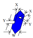
Point defect, Black spot, dust (including Polarizer)
j = (X+Y)/2 |

Unit: Inch2
|
|||||||||||||
| 4 | Line defect, Scratch | 
Unit: mm
|
|||||||||||||
|
5 |
Rainbow |
No more than two color changes across the viewing area. | |||||||||||||

| No. | Item | Criterion | ||||||||
| 7 | Segment pattern
W = Segment width j = (X+Y)/2 |
(1) Pinhole
j < 0.10mm is acceptable. Unit: mm
|
||||||||
| 8 | Back-light | (1) The color of the backlight should match with the specification.
(2) Not allow flickering |
||||||||
| 9 | Soldering | (1) Not allow heavy dirty and solder balls on PCB. (The size of dirty refers to point and dust defect)
(2) Over 50% of lead should be soldered on Land.
|
||||||||
| 10 | Wire | (1) Copper wire should not be rusted
(2) Do Not allow cracks on the copper wire connection. (3) Not allow reversing the position of the flat cable. (4) Not allow exposed copper wire inside the flat cable. |
||||||||
| 11* | PCB | (1) Not allow screw rust or damage.
(2) Not allow missing or wrong putting of components. |

Reliability of LCM
Reliability test condition:
| Item | Condition | Time (hrs) | Assessment |
| High temp. Storage | 80°C | 48 | No abnormalities in functions and appearance |
| High temp. Operating | 70°C | 48 | |
| Low temp. Storage | -30°C | 48 | |
| Low temp. Operating | -20°C | 48 | |
| Humidity | 40°C/ 90%RH | 48 | |
| Temp. Cycle | 0°C ¬ 25°C ®50°C
(30 min ¬ 5 min ® 30min) |
10cycles |
Recovery time should be 24 hours minimum. Moreover, functions, performance, and appearance shall be free from remarkable deterioration within 50,000 hours under ordinary operating and storage conditions at room temperature (20+8°C), normal humidity (below 65% RH), and in the area not exposed to direct sunlight.
Precaution for using LCD/LCM
- LCD/LCM is assembled and adjusted with a high degree of precision.
- Do not attempt to make any alteration or modification.
- The following should be noted.
General Precautions:
- LCD panel is made of glass. Avoid excessive mechanical shock or applying strong pressure onto the surface of the display area.
- The polarizer used on the display surface is easily scratched and damaged. Extreme care should be taken when handling. To clean dust or dirt off the display surface, wipe gently with cotton, or other soft material soaked with isopropyl alcohol, ethyl alcohol, or trichloro tri florothane, do not use water, ketone, or aromatics, and never scrub hard.
- Do not tamper in any way with the tabs on the metal frame.
- Do not make any modification on the PCB without consulting XIAMEM OCULAR
- When mounting an LCM, make sure that the PCB is not under any stress such as bending or twisting. Elastomer contacts are very delicate and missing pixels could result from slight dislocation of any of the elements.
- Avoid pressing on the metal bezel, otherwise the elastomer connector could be deformed and lose contact, resulting in missing pixels and also causing a rainbow on the display.
- Be careful not to touch or swallow liquid crystals that might leak from a damaged cell. If any liquid crystal spreads to the skin or clothes, wash it off immediately with soap and water.
Static Electricity Precautions:
- CMOS-LSI is used for the module circuit; therefore operators should be grounded whenever he/she comes into contact with the module.
- Do not touch any of the conductive parts such as the LSI pads; the copper leads on the PCB and the interface terminals with any parts of the human body.
- Do not touch the connection terminals of the display with bare hands; it will cause disconnection or defective insulation of terminals.
- The modules should be kept in anti-static bags or other containers resistant to static for storage.
- Only properly grounded soldering irons should be used.
- If an electric screwdriver is used, it should be grounded and shielded to prevent sparks.
- The normal static prevention measures should be observed for work clothes and working benches.
- Since dry air is inductive to static, a relative humidity of 50-60% is recommended.
Soldering Precautions:
- Soldering should be performed only on the I/O terminals.
- Use soldering irons with proper grounding and no leakage.
- Soldering temperature: 280°C+10°C
- Soldering time: 3 to 4 seconds.
- Use eutectic solder with resin flux filling.
- If the flux is used, the LCD surface should be protected to avoid spattering flux.
- Flux residue should be removed.
Operation Precautions:
- The viewing angle can be adjusted by varying the LCD driving voltage Vo.
- Since applied DC voltage causes electrochemical reactions, which deteriorate the display, the applied pulse waveform should be symmetric such that no DC component remains. Be sure to use the specified operating voltage.
- Driving voltage should be kept within a specified range; excess voltage will shorten display life.
- Response time increases with a decrease in temperature.
- Display color may be affected at temperatures above its operational range.
- Keep the temperature within the specified range of usage and storage. Excessive temperature and humidity could cause polarization degradation, polarizer peel-off or generate bubbles.
- For long-term storage over 40°C is required, the relative humidity should be kept below 60%, and avoid direct sunlight.
Documents / Resources
 |
Handson Technology DSP-1165 I2C Serial Interface 20x4 LCD Module [pdf] User Guide DSP-1165 I2C Serial Interface 20x4 LCD Module, DSP-1165, I2C Serial Interface 20x4 LCD Module, Interface 20x4 LCD Module, 20x4 LCD Module, LCD Module, Module |
