![]() Gowin Advanced FIR Filter IP
Gowin Advanced FIR Filter IP
User Guide
Advanced FIR Filter IP Software
Copyright © 2022 Guangdong Gowin Semiconductor Corporation. All Rights Reserved.
is a trademark of Guangdong Gowin Semiconductor Corporation and are registered in China, the U.S. Patent and Trademark Office, and other countries. All other words and logos identified as trademarks or service marks are the property of their respective holders. No part of this document may be reproduced or transmitted in any form or by any denotes, electronic, mechanical, photocopying, recording or otherwise, without the prior written consent of GOWINSEMI.
Disclaimer
GOWINSEMI assumes no liability and provides no warranty (either expressed or implied) and is not responsible for any damage incurred to your hardware, software, data, or property resulting from usage of the materials or intellectual property except as outlined in the GOWINSEMI Terms and Conditions of Sale. All information in this document should be treated as preliminary. GOWINSEMI may make changes to this document at any time without prior notice. Anyone relying on this documentation should contact GOWINSEMI for the current documentation and errata.
Revision History
| Date | Version | Description |
| 1/15/2019 | 1.0E | Initial version published. |
| 8/30/2019 | 1.1E | FIR structure updated and FIR three modes integrated. |
| 4/6/2021 | 1.2E | •The description of Initialization coefficient file updated. •Read and write timing descriptions updated. |
| 11/17/2022 | 2.0E | FIR Filter structures added. |
About This Guide
1.1 Purpose
The purpose of Gowin Advanced FIR Filter IP User Guide is to help you learn the features and usage of Gowin Advanced FIR Filter IP by providing the descriptions of functions, ports, timing, GUI and reference design, etc.
1.2 Related Documents
The latest user guides are available on the GOWINSEMI Website. You can find the related documents at www.gowinsemi.com:
- DS100, GW1N series FPGA Products Data Sheet
- DS117, GW1NR series of FPGA Products Data Sheet
- DS102, GW2A series of FPGA Products Data Sheet
- DS976, GW2AN-55 Data Sheet
- DS961, GW2ANR series of FPGA Products Data Sheet
- DS226, GW2AR series of FPGA Products Data Sheet
- SUG100, Gowin Software User Guide
1.3 Terminology and Abbreviations
The terminology and abbreviations used in this manual are as shown in Table 1-1 Terminology and Abbreviations.
Table 1-1 Terminology and Abbreviations
| Terminology and Abbreviations | Meaning |
| FIR | Finite Impulse Response |
| FPGA | Field Programmable Gate Array |
| IP | Intellectual Property |
| SRAM | Static Random Access Memory |
1.4 Support and Feedback
Gowin Semiconductor provides customers with comprehensive technical support. If you have any questions, comments, or suggestions, please feel free to contact us directly by the following ways.
Website: www.gowinsemi.com
E-mail: support@gowinsemi.com
Overview
2.1 Gowin Advanced FIR Filter IP Introduction
Gowin Advanced FIR Filter IP can implement Finite Impulse Response (FIR) filter function. According to different types of FIR filters, it supports configurations in four modes, and supports multi-channel processing and time-division multiplexing processing.
Table 2-1 Gowin Advanced FIR Filter IP
| Gowin Advanced FIR Filter IP | |
| IP Core Application | |
| Logic Resource | Please refer to Table 3-1,Table 3-2,Table 3-3. and Table 3-4. |
| Delivered Doc. | |
| Design Files | Verilog (encrypted) |
| Reference Design | Verilog |
| TestBench | Verilog |
| Test and Design Flow | |
| Synthesis Software | GowinSynthesis |
| Application Software | Gowin Software (V1.9.8.09 and above) |
Note!
For the devices supported, you can click here to get the information.
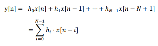
2.2 FIR Filter Algorithm Introduction
The calculation formula of Finite Impulse Response Filter is as follows:
y[n] = ℎ0?[?] + ℎ1?[? − 1] + ⋯ + ℎ?−1?[? − ? + 1]
![]()
Gowin Advanced FIR Filter IP is optimized according to the characteristics of filter coefficients for different working modes.
2.3 FIR Singlerate Structure and Function
FIR Singlerate mode implements FIR filter by transposition structure; the input/output is processed by pipeline, and the result can be obtained quickly, which is suitable for designs with large data and coefficient bit width but relatively small order. The basic structure is as shown in Figure
2-1. Figure 2-1 FIR Singlerate Structure

2.4 FIR Symmetry Structure and Function
FIR Symmetry mode is designed based on FIR coefficient symmetry, which can save half of the resources such as multipliers. The basic structure is as shown in Figure 2-2.

2.5 FIR Polyphase Decimator Structure and Function
FIR Polyphase Decimator is designed with a polyphase filter structure to implement filtering and downsampling functions. The basic structure is as shown in Figure 2-3.

2.6 FIR Polyphase Interpolator Structure and Function
FIR Polyphase Interpolator is designed with a polyphase filter structure to implement filtering and downsampling functions. The basic structure is as shown in Figure 2-4.
Figure 2-4 FIR Polyphase Interpolator Structure

Features and Performance
3.1 Features
- Supports 4 FIR types
- Supports input data width 2-18 bits
- Supports coefficient bit width 2-18 bits
- Supports output data bit width 2-37 bits
- Supports number of taps 2-1024 (depending on chip resource)
- Supports number of channels 1-8 (depending on chip resource)
- Supports time-division multiplexing
3.2 Max. Frequency
The maximum frequency of Gowin Advanced FIR Filter IP is mainly determined by the speed grade of the devices and configuration parameters.
3.3 Latency
The latency of Gowin Advanced FIR Filter IP is determined by the configuration parameters.
3.4 Resource Utilization
Its performance and resource utilization may vary when the design is employed in different devices, or at different densities, speed grades or in different IP configuration modes.
Take GW2A-18 series of FPGA as an example. See Table 3-1,Table 3-2,Table 3-3, and Table 3-4 for the resource utilization. For the applications on the other GOWINSEMI devices, please refer to the later release.
Table 3-1 Resource Utilization in FIR Singlerate Mode
| Device | Speed Grade |
Name | Resource Utilization |
Note |
| GW2A-18 | -7 | Registers | 10118 | Din Width=16, Coeff Width= 8 Dout Width = 31 Taps Size = 128 Input Channel = 3 TDM = 4 |
| LUT | 5537 | |||
| ALU | 1486 | |||
| DSP | 32 | |||
| BSRAM | 1 | |||
| SRAM | 128 |
Table 3-2 Resource Utilization in FIR Symmetry Mode
| Device | Speed Grade |
Name | Resource Utilization |
Note |
| Registers | 8885 | |||
| LUT | 4760 | Din Width=16, Coeff Width= 8 | ||
| GW2A-18 | -7 | ALU | 1055 | Dout Width = 31 |
| Taps Size = 128 | ||||
| DSP | 16 | Input Channel = 3 | ||
| BSRAM | 1 | TDM = 4 | ||
| SRAM | 64 |
Table 3-3 Resource Utilization in FIR Polyphase Decimator Mode
| Device | Speed Grade | Name | Resource Utilization |
Note |
| GW2A-18 | -7 | Registers | 9281 | Din Width=16, Coeff Width= 8 Dout Width = 31 TapsSize = 128 Input Channel = 3 TDM = 4 Factor = 2 |
| LUT | 5207 | |||
| ALU | 792 | |||
| DSP | 16 | |||
| BSRAM | 1 | |||
| SRAM | 72 |
Table 3-4 Resource Utilization in FIR Polyphase Interpolator Mode
| Device | Speed Grade |
Name | Resource Utilization |
Note |
| GW2A-18 | -7 | Registers | 5322 | Din Width=16, Coeff Width= 8 Dout Width = 31 TapsSize = 128 Input Channel = 3 TDM = 4 Factor = 2 |
| LUT | 2819 | |||
| ALU | 737 | |||
| DSP | 16 | |||
| BSRAM | 1 | |||
| SRAM | 64 |
Port Description
Gowin Advanced FIR Filter IP Ports
The details of Gowin Advanced FIR Filter IP I/O ports are shown in Figure 4-1.
Figure 4-1 Gowin Advanced FIR Filter IP Port Diagram 
The details of Gowin Advanced FIR Filter IP I/O ports are shown in
Table 4-1.
Table 4-1 Port List
| Signal | I/O | Data Width | Description |
| clk | I | 1 | Clock signal |
| rstn | I | 1 | Reset signal, active-low. |
| fir_valid_i | I | 1 | Data input valid signal |
| fir_sync_i | I | 1 | Data channel synchronization signal, |
Timing Description
This chapter introduces the timing of Gowin Advanced FIR Filter.
Gowin Advanced FIR Filter IP Timing
Figure 5-1 shows the data input timing diagram of Gowin Advanced FIR Filter IP.
Figure 5-1 Data Input Timing Diagram of Advanced FIR Filter IP with 3 Channels and Time Division Multiplexing 3

- After the signal fir_rfi_o is pulled up, input data, and data can be input continuously or at intervals.
- When the signal fir_valid_i is high, the input data is valid.
- When the signal fir_sync_i is high, it means that this is the first channel data. After that, input the channel data in turn. If only one channel data is input, the signal fir_sync_i is pulled up as signal fir_valid_i is pulled up.
- When the last channel data is input, the signal fir_rfi_o is pulled down.
Then input data after the next pull up.
Figure 5-2 shows the data output timing diagram.
Figure 5-2 Data Output Timing Diagram of Advanced FIR Filter IP with 3 Channels and Time Division Multiplexing 3
- When the signal fir_valid_o is high, the data output is valid.
- When the signal fir_sync_o is high, it means that this is the first channel valid data. Then the data of channel 2, channel 3 and so on is output in turn.
- There are NUM_TDM (time division multiplexing value) intervals between each channel data.
Call and Configuration
You can select “Tools” in Gowin Software to start IP Core Generator to call and configure Advanced FIR Filter.
- Open IP Core Generator
After creating a new project, you can click the “IP Core Generator” button to open the IP Core Generator, as shown in Figure 6-1.

- Open Advanced FIR Filter IP Core
Double click “Math > Advanced FIR Filter” to open the interface of Gowin Advanced FIR Filter IP core, as shown in Figure 6-2.
Figure 6-2 Advanced FIR Filter IP Interface

- Descriptions of Initializing Coefficient File
Gowin Advanced FIR Filter IP supports coefficient initialization function. When Gowin Advanced FIR Filter IP is called, the initialization coefficient file must be specified. If the filter is as follows:
Then in the coefficient file, the data should be placed in the following position:
h0
h1
h2
…
hN-1
And the data is decimal plain text. The size of the initialization coefficient should be within the range of the selected coefficient bit width, and the number of initialization should be consistent with the number of FIR taps, otherwise the GUI will report a data error.
In the case of a multi-channel configuration, the data in the coefficient file should be placed:
Data 0 of channel 0 (Coeff00)
Data 1 of channel 0 (Coeff0,01)
Data N -1 of channel 0 (Coeff 0 N -1)
…
Data 0 of channel 1 (Coeff10)
Data 1 of channel 1 (Coeff 1 1)
…
Data N -1 of channel 1 (Coeff1,N-1)
Data 0 of channel M-1 (CoeffM-10)
Data 1 of channel M-1(CoeffM-11)
…
Data N-1 of channel M-1 (CoeffM-1 N-1 )
The FIR coefficient data format conversion can be generated by referring to the following MATLAB example.
Figure 6-3 MATLAB Example

Reference Design
This chapter is intended to introduce the usage and structure of the reference design of Gowin Advanced FIR Filter IP. Gowin Advanced FIR Filter IP design example has only one module. Please refer to reference design for details.
Application
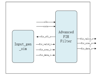
The block diagram of reference design is as shown in Figure 7-1. In the design instance, the steps are as follows:
- Through the input_gen_sim module, input data is generated for Advanced FIR Filter module.
- After the operation by IP, the output data is obtained.
Figure 7-1 Block Diagram of Reference Design
IP functions can be verified using this design. When the reference design is applied to board level testing, you need to provide appropriate stimulus to the reference design, and you can use an on-line logic analyzeror oscilloscope to observe the signals.
Documents / Resources
 |
GOWIN Advanced FIR Filter IP Software [pdf] User Guide IPUG543-2.0E, Advanced FIR Filter IP Software, FIR Filter IP Software, Filter IP Software, IP Software, Software |