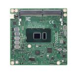
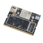
FDI SYG-S7G2-SOM System on Module

Product Usage Instructions
- Specifications
- Product Name: yG S7G2 System on Module (SOM)
- Interface: 200-pin SODIMM
- Compatibility: FDI’s yGTM Modular Development LCD Kits
- Power Requirement: 5V DC Center Positive 2A
- Power Load: 300mA typical, 475mA max load
- Product Overview
- The yG S7G2 System on Module (SOM) is designed to facilitate the integration of Renesas SynergyTM into various designs.
- It offers essential functions in a convenient SODIMM form factor, making it suitable for product development and custom applications.
- The module features an industry-standard 200-pin interface and is fully compatible with FDI’s yGTM Modular Development LCD Kits.
- ESD Warning
- When handling the yG S7G2 SOM, ensure to keep it in the protective anti-static package provided.
- Avoid exposing the module to high electrostatic potentials as this can lead to irreversible damage that may not be covered under warranty.
- Adhere to standard practices for working with static-sensitive components to prevent any mishaps.
- Powering the Module
- The yG S7G2 SOM receives power through the development kit. Use a 5V DC Center Positive 2A power supply for optimal performance. Ensure that the power load does not exceed 475mA to prevent any issues.
- Connecting ARM Mini-JTAG J2
- The module utilizes a JTAG connector based on a 2mm header called ARM Mini-JTAG J2. This connector offers the same functionality as a standard 20-pin JTAG connector but occupies less board space, making it efficient for use.
FAQs
- Q: What is the power requirement for the yG S7G2 SOM?
- A: The power requirement for the yG S7G2 SOM is a 5V DC Center Positive 2A power supply.
- Q: How should I handle static electricity when working with the module?
- A: Always keep the module in its anti-static package and follow standard practices for working with static-sensitive devices to prevent damage.
Important Legal Information
- Information in this document is provided solely to enable the use of Future Designs, Inc. (FDI) products. FDI assumes no liability whatsoever, including infringement of any patent or copyright. FDI reserves the right to make changes to these specifications at any time, without notice. No part of this document may be reproduced or transmitted in any form or by any means, electronic or mechanical, for any purpose, without the express written permission of Future Designs, Inc. 996 A Cleaner Way, Huntsville, AL 35805.
- NOTE: The inclusion of vendor software products in this kit does not imply an endorsement of the product by Future Designs, Inc.
yG™ is a trademark of Future Designs, Inc. - Renesas Synergy™ is a trademark of Renesas Electronics Corporation.
- Microsoft, MS-DOS, Windows, Windows XP, Microsoft Word are registered trademarks of Microsoft Corporation.
- Other brand names are trademarks or registered trademarks of their respective owners.
- Printed in the United States of America.
- For more information on FDI or our products please visit https://www.teamfdi.com.
- Document Rev 2.3 © 2018 Future Designs, Inc. All rights reserved.
ΣyG S7G2 System on Module (SOM) Overview
- Introduction
- The ΣyG S7G2 System on Module (SOM) provides a quick and easy solution for implementing Renesas SynergyTM into a design, by providing the basic functions necessary for a product on an easy to use SODIMM. The ΣyG S7G2 SOM uses an industry standard 200-pin SODIMM interface and is compatible with FDI’s ΣyGTM Modular Development LCD Kits. It can also be used for custom platform development or customer applications.
- ESD Warning
- The ΣyG S7G2 SOM is shipped in a protective anti-static package. Do not subject the module to high electrostatic potentials. Exposure to high electrostatic potentials may cause damage to the boards that will not be covered under warranty. General practice for working with static sensitive devices should be followed when working with the kit.
Renesas Synergy S7G2 Microcontroller Block Diagram

ΣyG S7G2 SOM System Block Diagram


Figure 2: ΣYG-S7G2 Kit Block Diagram (4.3” display shown)
Requirements
- The ΣyG S7G2 SOM requires a development kit such as the ΣyG S7G2 Modular Development Kit. Each yG development kit includes:
- ΣyG S7G2 System on Module (SOM)
- Renesas Synergy Software Platform
- Carrier Board
- 5 VDC, 2.3A North American Power Supply
- USB and Ethernet Cables
- Segger ARM Cortex-M Mini-JTAG debugger and cables
- Optional LCD Carrier Board
- Optional 4.3” or 7.0″ PCAP Touch Screen LCD
ΣyG S7G2 SOM Power Requirements
Power is supplied to the Yg S7G2 SOM through the development kit. The power requirement for all yG development kits is 5V DC Center Positive 2A Power Supply. The power load of the SOM is 300mA typical and 475mA max load.
ΣyG S7G2 SOM System on Module Board Components ARM Mini-JTAG J2
- The ΣyG-S7G2 SOM uses a JTAG connector based on a 2mm header.
- This smaller connector provides 100% of the functionality of the standard 20-pin JTAG connector but utilizes 70% less board space.
| Pin Number | Description | Pin Number | Description |
| 1 | VCC | 6 | TDO |
| 2 | TMS | 7 | X |
| 3 | GND | 8 | TDI |
| 4 | TCK | 9 | GND |
| 5 | GND | 10 | JST# |

Tag-Connect J7
Use the Tag Connect 10-pin cable to program and JTAG the ΣyG S7G2 SOM using a Segger J-Link device.
- Cable: https://www.tag-connect.com/tc2050-arm2010.
- Cable: https://www.tag-connect.com/TC2050-IDC-NL.

MicroSD Socket J1
The ΣyG S7G2 SOM utilizes a microSD for flexible mass storage. MicroSD flash cards are common, cost-effective, and provide a large amount of user-changeable memory.
| Pin Number | Description |
| 1 | DAT2/RSV |
| 2 | CD_DAT3/CS# |
| 3 | CMD/SDI |
| 4 | VDD |
| 5 | CLK/SCLK |
| 6 | VSS |
| 7 | DAT0/SDO |
| 8 | DAT1/RSV |
| 9 | CD |
NOTE: The microSD card must be removed using the spring loaded “push-pull” mechanism on the microSD socket. Forceful removal of a microSD card will result in permanent damage to the socket that is not covered under warranty. To insert the card, push it into the socket until a “click” sound is heard. Similarly, to remove the card, push the card into the socket. The push-pull mechanism will “click” again and eject the card from the socket. The card is now available for safe removal.
Inserting the microSD card into the microSD socket

Removing the microSD card from the microSD socket

Ethernet PHY U5
- The ΣyG S7G2 SOM provides an Ethernet PHY from SMSC, LAN8720. The LAN8720 is a single-chip solution for a 100BASE-TX/10BASE-T physical layer transceiver.
- It has support for reduced MII (RMII), and HP MDI-X auto crossover allowing for any standard Ethernet cable to be used, even a crossover cable.
- The LAN8720 is fully compliant with IEEE 802.3u with support for auto-negotiation and manual selection of 10/100Mbps speed as well as full and half-duplex modes.
200-pin SOMDIMM Connector Details J4
The SYG-S7G2-SOM utilizes a standard 200-pin SODIMM Interface supported by various socket manufacturers. The recommended socket is manufactured by TE Connectivity, PN: 1473005-4
| Pin | SOMDIMM Signal Name | Application Details | I/O | SOMDIMM Connection Details |
| 1 | ETH_TXP | Ethernet Transmit Positive | O | Output from KSZ8041 Ethernet PHY |
| 2 | ETH_RXP | Ethernet Receive Positive | I | Output from KSZ8041 Ethernet PHY |
| 3 | ETH_TXN | Ethernet Transmit Negative | O | Input to KSZ8041 Ethernet PHY |
| 4 | ETH_RXN | Ethernet Receive Negative | I | Input to KSZ8041 Ethernet PHY |
| 5 | 3V3A | 3.3V Analog | P | Analog 3.3V Output from PHY Circuit |
| 6 | GND | Ground | P | |
| 7 | ETH_LED0 | Ethernet LED0 | O | Ethernet LED0 output from KSZ8041 |
| 8 | ETH_LED1 | Ethernet LED1 | O | Ethernet LED1 output from KSZ8041 |
| 9 | VBAT_IN | Vdd Battery Input | P | Vdd for battery backup of internal RTC |
| 10 | NC | Not Connected | U | |
| 11 | RSTIN# | Reset Input | I | Reset input to POR IC TPS3801 |
| 12 | RST# | O | Reset output from POR circuit | |
| 13 | GPIO13_USB_ID | |||
| 14 | NC | Not connected | U | |
| 15 | NC | Not connected | U | |
| 16 | NC | Not connected | U | |
| 17 | NC | Not connected | U | |
| 18 | NC | Not connected | U | |
| 19 | NC | Not connected | U | |
| 20 | NC | Not connected | U | |
| 21 | AVCC | |||
| 22 | AVCC | |||
| 23 | AVSS | |||
| 24 | GND | Ground | P | |
| 25 | GPIO25_LCDPWR | LCD Power Enable | O | Connected to S7G2 Port 4 bit 9 * |
| 26 | GPIO26_LCDLE | LCD Latch Enable | O | Connected to S7G2 Port 4 bit 15 * |
| 27 | GPIO27_LCDCLK | LCD Clock | O | Connected to S7G2 Port 9 bit 0 * |
| 28 | GPIO28_LCDFP | O | Connected to S7G2 Port 3 bit 14 * | |
| 29 | GPIO29_LCDEN | O | Connected to S7G2 Port 3 bit 13 * | |
| 30 | GPIO30_LCDLP | O | Connected to S7G2 Port 3 bit 15 * | |
| 31 | GPIO31_LCDVDR4 | LCD Data Bit 4 (Red) | O | Connected to S7G2 Port 9 bit 8 * |
| 32 | GPIO32_LCDVDR5 | LCD Data Bit 5 (Red) | O | Connected to S7G2 Port 9 bit 1 * |
| 33 | GPIO33_LCDVDR6 | LCD Data Bit 6 (Red) | O | Connected to S7G2 Port 5 bit 13 * |
| 34 | GPIO34_LCDVDR7 | LCD Data Bit 7 (Red) | O | Connected to S7G2 Port 8 bit 5 * |
| 35 | GPIO35_SSLB2 | GPIO SPI Slave Select 2 Channel B | U | Connected to S7G2 Port 2 bit 7 * |
| 36 | GPIO36 | GPIO (used for LCD SPI Chip Select) | U | Connected to S7G2 Port 4 bit 14 * |
| 37 | 3.3V | 3.3V Power | P | |
| 38 | GND | Ground | P | |
| 39 | 3.3V | 3.3V Power | P | |
| 40 | GND | Ground | P | |
| 41 | USBH_DP | USB Host Data Positive | B | Connected to S7G2 USB Port A D+ |
| 42 | USBD_DP | USB Device Data Positive | B | Connected to S7G2 USB Port B D+ |
| 43 | USBH_DM | USB Host Data Negative | B | Connected to S7G2 USB Port A D- |
| 44 | USBD_DM | USB Device Data Negative | B | Connected to S7G2 USB Port B D- |
| 45 | GPIO45_LCD_B2 | LCD Data Bit 2 (Blue) | O | Connected to S7G2 Port 8 bit 4 * |
| 46 | GPIO46_LCD_B3 | LCD Data Bit 3 (Blue) | O | Connected to S7G2 Port 8 bit 3 * |
| 47 | GPIO47_RD | GPIO / CAN Receive Data | I | Connected to S7G2 Port 8 bit 12 * |
| 48 | GPIO48_TD | GPIO / CAN Transmit Data | O | Connected to S7G2 Port 8 bit 11 * |
| 49 | GPIO49 | GPIO | B | Connected to S7G2 Port 6 bit 0 * |
| 50 | NC | Not connected | U | |
| 51 | GPIO51_SPCK | GPIO / SPI Clock | O | Connected to S7G2 Port A bit 4 * |
| 52 | GPIO52 | GPIO | B | Connected to S7G2 Port A bit 5 * |
| 53 | GPIO53_MISO | GPIO / SPI Master In/Slave Out | I | Connected to S7G2 Port A bit 3 * |
| 54 | GPIO51_SPCK | GPIO / Connected to pin 51 | ||
| 55 | GPIO55 | GPIO | B | Connected to S7G2 Port A bit 6 * |
| Pin | SOMDIMM Signal Name | Application Details | I/O | SOMDIMM Connection Details |
| 56 | GPIO56_MOSI | GPIO / SPI Master Output Salve Input | Connected to S7G2 Port A bit 2 * | |
| 57 | GPIO57_TXD | GPIO / Serial Transmit Data – For RS232 | O | Connected to S7G2 Port 5 bit 9 * |
| 58 | GPIO58_RXD | GPIO / Serial Receive Data – For RS232 | I | Connected to S7G2 Port 5 bit 10 * |
| 59 | NC | Not connected | U | DO NOT USE! |
| 60 | GPIO60_USBD_UPLED | GPIO / USB Device Up LED | O | Connected to S7G2 Port 9 bit 11 * |
| 61 | GPIO61_USBD_CON | GPIO / USB Device Connect | O | Connected to S7G2 Port 9 bit 12 * |
| 62 | GPIO62_RSCK | GPIO / SPI Clock | O | Connected to S7G2 Port 2 bit 4 * |
| 63 | GPIO63 | GPIO | O | Connected to S7G2 Port 0 bit 11 * |
| 64 | GPIO64_MISO | GPIO / SPI MISO | I | Connected to S7G2 Port 2 bit 2 * |
| 65 | GPIO65_MOSI | GPIO / SPI MOSI | O | Connected to S7G2 Port 2 bit 3 * |
| 66 | GPIO66 | GPIO | B | Connected to S7G2 Port 5 bit 11 * |
| 67 | GPIO67 | GPIO | B | Connected to S7G2 Port 5 bit 12 * |
| 68 | GPIO68_USBH_OVC | GPIO / USB Host Over Current | I | Connected to S7G2 Port 7 bit 6 * |
| 69 | GPIO69_TPIRQ | GPIO / Touch IC IRQ15 Input | B | Connected to S7G2 Port 5 bit 6 * |
| 70 | GPIO70_AD0.0 | GPIO / AD0 Bit 0 | I | Connected to S7G2 Port 0 bit 0 * |
| 71 | GPIO71_AD0.1 | GPIO / AD0 Bit 1 | I | Connected to S7G2 Port 0 bit 9 * |
| 72 | GPIO72_AD0.2 | GPIO / AD0 Bit 2 | I | Connected to S7G2 Port 0 bit 5 * |
| 73 | GPIO73_AD0.5_DA1 | GPIO / AD0 Bit 3 / DAC Output 1 | B | Connected to S7G2 Port 0 bit 15 * |
| 74 | GPIO74_SDA | GPIO / User IO I2C Bus SDA | B | Connected to S7G2 Port 4 bit 1 * |
| 75 | GPIO75_SCL | GPIO / User IO I2C Bus SCL | O | Connected to S7G2 Port 4 bit 0 * |
| 76 | GND | Ground | P | |
| 77 | GND | Ground | P | |
| 78 | GPIO78_ACC_IRQ | GPIO / Accelerometer IRQ | I | Connected to S7G2 Port 7 bit 7 * |
| 79 | NC | |||
| 80 | GPIO80_RTC_IRQ | GPIO / RTC IRQ Input | I | Connected to S7G2 Port 0 bit 1 * |
| 81 | NC | Not connected | U | |
| 82 | NC | Not connected | U | |
| 83 | NC | Not connected | U | |
| 84 | NC | Not connected | U | |
| 85 | NC | Not connected | U | |
| 86 | GPIO86_LED_BR | GPIO / LCD Backlight Brightness PWM | B | Connected to S7G2 Port A bit 7 * |
| 87 | GPIO87_USBH_PPWR | GPIO / USB Host Power (Inverted output) | O | Connected to S7G2 Port B bit 0 * |
| 88 | GPIO88_LCD_G2 | LCD Data Bit 2 (Green) | O | Connected to S7G2 Port A bit 1 * |
| 89 | GPIO89_LCD_G3 | LCD Data Bit 3 (Green) | O | Connected to S7G2 Port A bit 10 * |
| 90 | GPIO90_LCD_G4 | LCD Data Bit 4 (Green) | O | Connected to S7G2 Port A bit 9 * |
| 91 | GPIO91_LCD_G5 | LCD Data Bit 5 (Green) | O | Connected to S7G2 Port A bit 8 * |
| 92 | GPIO92_LCD_G6 | LCD Data Bit 6 (Green) | O | Connected to S7G2 Port 6 bit 15 * |
| 93 | GPIO93_LCD_G7 | LCD Data Bit 7 (Green) | O | Connected to S7G2 Port 9 bit 5 * |
| 94 | GPIO94_LCD_B4 | LCD Data Bit 4 (Blue) | O | Connected to S7G2 Port 8 bit 2 * |
| 95 | GPIO95_LCD_B5 | LCD Data Bit 5 (Blue) | O | Connected to S7G2 Port 6 bit 6 * |
| 96 | GPIO96_LCD_B6 | LCD Data Bit 6 (Blue) | O | Connected to S7G2 Port 6 bit 7 * |
| 97 | GPIO97_LCD_B7 | LCD Data Bit 7 (Blue) | O | Connected to S7G2 Port A bit 0 * |
| 98 | GPIO98_USBD_VBUS | USB Device VBus Sense Input | I | Connected to S7G2 Port 4 bit 7 * |
| 99 | GPIO99_AD0 | GPIO / AD0 | Connected to S7G2 Port 0 bit 2 * | |
| 100 | NC | Not connected | B | Unused |
| 101 | GND | Ground | P | |
| 102 | GND | Ground | P | |
| 103 | NC | Not connected | U | Unused |
| 104 | NC | Not connected | U | Unused |
| 105 | NC | Not connected | U | Unused |
| 106 | NC | Not connected | U | Unused |
| 107 | NC | Not connected | U | Unused |
| 108 | NC | Not connected | U | Unused |
| 109 | NC | Not connected | U | Unused |
| 110 | NC | Not connected | U | Unused |
| 111 | NC | Not connected | U | Unused |
| 112 | NC | Not connected | U | Unused |
| 113 | 5V0 | 5.0V Power | P | |
| 114 | 5V0 | 5.0V Power | P | |
| 115 | NC | Not connected | U | Unused |
| 116 | GPIO116 | GPIO | B | Connected to S7G2 Port 5 bit 14 * |
| Pin | SOMDIMM Signal Name | Application Details | I/O | SOMDIMM Connection Details |
| 117 | GPIO117 | GPIO | B | Connected to S7G2 Port 5 bit 15 * |
| 118 | GPIO118 | GPIO | B | Connected to S7G2 Port B bit 2 * |
| 119 | GPIO119 | GPIO | B | Connected to S7G2 Port B bit 3 * |
| 120 | GPIO120 | GPIO | B | Connected to S7G2 Port 8 bit 6 * |
| 121 | GPIO121 | GPIO | B | Connected to S7G2 Port 8 bit 7 * |
| 122 | GPIO122 | GPIO | B | Connected to S7G2 Port 8 bit 8 * |
| 123 | GPIO123_SPKR_DA0 | GPIO / DAC Output 0 | B | Connected to S7G2 Port 0 bit 14 * |
| 124 | GPIO124 | GPIO | B | Connected to S7G2 Port 8 bit 9 * |
| 125 | GPIO125 | GPIO | B | Connected to S7G2 Port 8 bit 10 * |
| 126 | GPIO126 | GPIO | B | Connected to S7G2 Port 9 bit 13 * |
| 127 | GPIO127_LCD_R2 | LCD Data Bit 2 (Red) | B | Connected to S7G2 Port 9 bit 6 * |
| 128 | GPIO128_LCD_R3 | LCD Data Bit 3 (Red) | B | Connected to S7G2 Port 9 bit 7 * |
| 129 | GND | Ground | P | |
| 130 | GND | Ground | P | |
| 131 | GPIO131_LCD18B | GPIO / Unused LCD Signal 18 | B | Connected to S7G2 Port A bit 11 * |
| 132 | GPIO132_LCD19B | GPIO / Unused LCD Signal 19 | B | Connected to S7G2 Port 9 bit 14 * |
| 133 | GPIO133_LCD20B | GPIO / Unused LCD Signal 20 | B | Connected to S7G2 Port 9 bit 15 * |
| 134 | GPIO134_LCD21B | GPIO / Unused LCD Signal 21 | B | Connected to S7G2 Port 9 bit 9 * |
| 135 | GPIO135_LCD22B | GPIO / Unused LCD Signal 22 | B | Connected to S7G2 Port 9 bit 10 * |
| 136 | GPIO136_LCD23B | GPIO / Unused LCD Signal 23 | B | Connected to S7G2 Port 9 bit 2 * |
| 137 | NC | Not connected | U | Unused |
| 138 | GPIO138 | GPIO | B | Connected to S7G2 Port 0 bit 6 * |
| 139 | GPIO139 | GPIO | B | Connected to S7G2 Port 0 bit 7 * |
| 140 | NC | Not connected | U | Unused |
| 141 | GPIO141 | GPIO | B | Connected to S7G2 Port 9 bit 4 * |
| 142 | GPIO142 | GPIO | B | Connected to S7G2 Port 8 bit 13 * |
| 143 | GPIO143 | GPIO | B | Connected to S7G2 Port A bit 12 * |
| 144 | GPIO144 | GPIO | B | Connected to S7G2 Port A bit 13 * |
| 145 | GPIO145 | GPIO | B | Connected to S7G2 Port A bit 14 * |
| 146 | GPIO146 | GPIO | B | Connected to S7G2 Port A bit 15 * |
| 147 | GPIO147 | GPIO | B | Connected to S7G2 Port B bit 1 * |
| 148 | GPIO148 | GPIO | B | Connected to S7G2 Port B bit 6 * |
| 149 | GPIO149_RX | GPIO / RS422/485 Receive Data | B | Connected to S7G2 Port B bit 5 * |
| 150 | GPIO150_TX | GPIO / RS422/485 Transmit Data | B | Connected to S7G2 Port B bit 4 * |
| 151 | GPIO151 | GPIO | B | Connected to S7G2 Port 5 bit 7 * |
| 152 | GPIO152 | GPIO | B | Connected to S7G2 Port 5 bit 8 * |
| 153 | GPIO153 | GPIO | B | Connected to S7G2 Port 0 bit 10 * |
| 154 | NC | Not connected | U | Unused |
| 155 | NC | Not connected | U | Unused |
| 156 | NC | Not connected | U | Unused |
| 157 | NC | Not connected | U | Unused |
| 158 | NC | Not connected | U | Unused |
| 159 | NC | Not connected | U | Unused |
| 160 | GPIO160_MD | GPIO /Boot Mode Input (not recommended for use) | B | Connected to S7G2 Port 2 bit 1 * |
| 161 | NC | Not connected | U | Unused |
| 162 | GPIO162_NMI | GPIO / Non-Maskable Interupt (not recommended for use) | U | Connected to S7G2 Port 2 bit 0 * |
| 163 | GND | Ground | P | |
| 164 | GND | Ground | P | |
| 165 | 3.3V | 3.3V Power | P | |
| 166 | GND | Ground | P | |
| 167 | NC | Not connected | U | Unused |
| 168 | NC | Not connected | U | Unused |
| 169 | NC | Not connected | U | Unused |
| 170 | NC | Not connected | U | Unused |
| 171 | NC | Not connected | U | Unused |
| 172 | NC | Not connected | U | Unused |
| 173 | NC | Not connected | U | Unused |
| 174 | NC | Not connected | U | Unused |
| 175 | NC | Not connected | U | Unused |
| Pin | SOMDIMM Signal Name | Application Details | I/O | SOMDIMM Connection Details |
| 176 | NC | Not connected | U | Unused |
| 177 | NC | Not connected | U | Unused |
| 178 | NC | Not connected | U | Unused |
| 179 | NC | Not connected | U | Unused |
| 180 | NC | Not connected | U | Unused |
| 181 | NC | Not connected | U | Unused |
| 182 | NC | Not connected | U | Unused |
| 183 | NC | Not connected | U | Unused |
| 184 | NC | Not connected | U | Unused |
| 185 | NC | Not connected | U | Unused |
| 186 | NC | Not connected | U | Unused |
| 187 | NC | Not connected | U | Unused |
| 188 | NC | Not connected | U | Unused |
| 189 | NC | Not connected | U | Unused |
| 190 | NC | Not connected | U | Unused |
| 191 | NC | Not connected | U | Unused |
| 192 | NC | Not connected | U | Unused |
| 193 | NC | Not connected | U | Unused |
| 194 | TMS | GPIO / JTAG Interface | I | Connected to S7G2 Port 1 bit 8 * |
| 195 | TCK | GPIO / JTAG Interface | I | Connected to S7G2 Port 3 bit 0 * |
| 196 | TDO | GPIO / JTAG Interface | O | Connected to S7G2 Port 1 bit 9 * |
| 197 | TDI | GPIO / JTAG Interface | I | Connected to S7G2 Port 1 bit 10 * |
| 198 | NC | Not connected | U | Unused |
| 199 | 3.3V | 3.3V Power | P | |
| 200 | GND | Ground | P |
updated pinout in Rev 2.2 document
ΣyG S7G2 System on Module Board Layout Schematics
- Visit this link for schematics of the SYG-S7G2-SOM: https://www.teamfdi.com/wp-content/uploads/SYG-S7G2-SOM.pdf.
Board Layout


Support
Where to Get Help
- Online technical support is available at https://www.teamfdi.com/support/.
Useful Links
- Future Designs, Inc. Forums: https://www.teamfdi.com/?post_type=forum.
- SYG-S7G2-SOM Product Page: https://www.teamfdi.com/product-details/syg-s7g2-som/.
- Renesas Synergy: https://synergybeta.renesas.com/.
- SEGGER J-Link LITE: https://www.segger.com/jlink-lite-cortexm.html.
- Renesas Forums: https://www.renesasrulz.com/.
Rev 2.3 Copyright ©2024, Future Designs, Inc.
Documents / Resources
 |
FDI SYG-S7G2-SOM System on Module [pdf] User Manual SYG-S7G2-SOM System on Module, SYG-S7G2-SOM, System on Module, on Module, Module |