EBYTE STM32WLE5CCU6C 920 MHz SoC SMD Module
Product Usage Instructions
Basic Operations
To begin using the E77-900M22S wireless communication module, follow these basic steps:
- Ensure the module is properly connected to the power supply within the specified range of 1.8~3.6V.
- Implement the necessary secondary development as required for your application.
- For optimal performance, consider utilizing dual antennas (optional) for enhanced signal reception.
- Refer to the user manual for detailed pin definitions and mechanical dimensions.
Application Scenarios
The E77-900M22S wireless communication module is suitable for various application scenarios, including:
- Home security alarm and remote keyless entry systems
- Smart home and industrial sensor networks
- Wireless alarm security systems
- Building automation solutions
- Wireless industrial-grade remote control applications
- Advanced Meter Reading Architecture (AMI)
- Automotive industry applications
Chapter 1 Overview
Introduction
E77-900M22S is based on ST’s newly launched STM32WLE5CCU6 (ARM Cortex-M4 + GFSK) SoC wireless communication module. It has the characteristics of long communication distance, low standby power consumption, strong anti-interference ability, rich interface resources, strong processing ability and small size. . And suitable for 920MHz frequency band SMD wireless module, using industrial-grade high-precision 32.768kHz and 32MHz crystal oscillator.
The E77-900M22S wireless communication module requires secondary development by the user, and can be widely used in the Internet of Things industry, especially suitable for the application development of WAN.
Features
- Under ideal conditions, the communication distance can reach 500m;
- The maximum transmit power is 6.0dBm, and the software is multi-level adjustable;
- Support global license-free ISM 920MHz frequency band;
- New SF5, SF7, SF8, SF11 spreading factor introduced to support dense network;
- Support 1.8~3.6V power supply, and the best performance can be guaranteed if the power supply is greater than 3.3V;
- The external crystal oscillator uses 32.768kHz, 32MHz high-precision industrial-grade crystal oscillator;
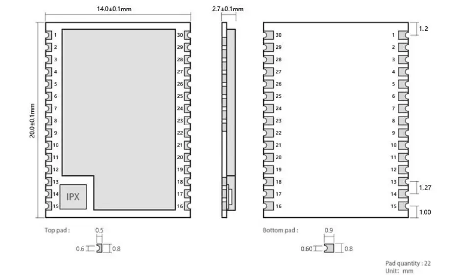
- 14.0*20.0*2.7mm small size SMD package, which is conducive to system integration development;
- Industrial standard design, support long-term use at -40 ~ +85 ℃;
- Dual antennas are optional (IPEX/stamp hole), which is convenient for users’ secondary development and integration;
Application scenarios
- Home security alarm and remote keyless entry
- Smart home and industrial sensors, etc.
- Wireless alarm security system
- Building automation solutions
- Wireless industrial grade remote control
- Advanced Meter Reading Architecture (AMI)
- Automotive industry applications.
Chapter 2 Specifications
RF parameters
| RF parameters | parameters | notes |
| Working frequency | 920.3–924.8 MHz | Support ISM band |
| transmit power | 0~6 dBm | The software is adjustable, and users need to develop their own settings |
| Receive sensitivity | -118 dBm | GFSK,air speed 500kbps |
| Spreading factor | 5~12 | —— |
| Measured distance | 500m | Clear and open environment, maximum power, antenna gain 4.36dBi, height 2m,
airspeed 500kbps |
Hardware parameters
| Hardware parameters | parameters | notes |
| IC full name | STM32WLE5CCU6 | —— |
| Core | Cortex-M4 | —— |
| FLASH | 256 kB | —— |
| RAM | 64 kB | —— |
| Crystal frequency | 32 MHz/32.768 kHz | External crystal |
| Size | 14 * 20 mm | —— |
| Antenna type | RSP-SMA-K | Equivalent Impedance Approx.50Ω |
| Communication interface | UART、SPI、I²C、GPIO、ADC | Users need to develop their own settings |
| Packaging | Patch stamp hole | —— |
Electrical parameters
| Electrical parameters | Min. | Typical valuev | Max. | unit | condition |
| voltage | 1.8 | 3.3 | 3.6 | V | ≥3.3V Guaranteed output power
Exceeding 3.6V will permanently burn the module |
| communication level | – | 3.3 | – | V | Using 5.0V TTL is recommended to add level conversion |
| Emission current | – | 128 | – | mA | Instantaneous power consumption |
| receive current | – | 14 | – | mA | —— |
| sleep current | – | 3 | – | μ A | software shutdown |
| Operating temperature | -40 | 20 | 85 | ℃ | —— |
| Working humidity | 10 | 60 | 90 | % | —— |
| Storage temperature | -40 | 20 | 125 | ℃ | —— |
Chapter 3 Mechanical Dimensions and Pin Definition
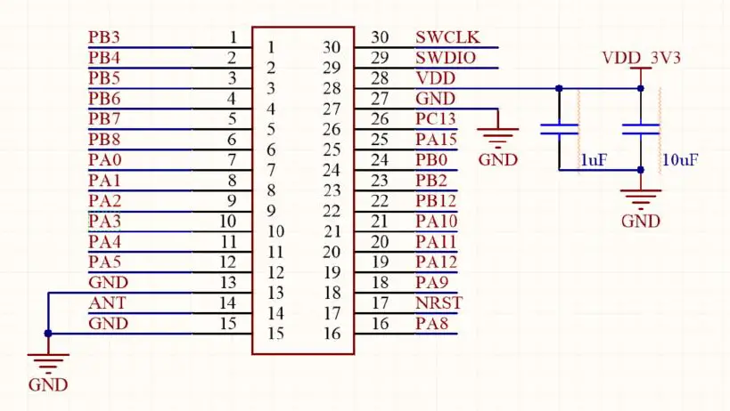
| pin number | Pin name | Pin direction | Pin | use | |
| 1 | PB3 | Input | /Output | Configurable general-purpose IO port (see STM32WLE5CCU6 manual for details) | |
| 2 | PB4 | Input | /Output | Configurable general-purpose IO port (see STM32WLE5CCU6 manual for details) | |
| 3 | PB5 | Input | /Output | Configurable general-purpose IO port (see STM32WLE5CCU6 manual for details) | |
| 4 | PB6 | Input | /Output | USART1_TX | |
| 5 | PB7 | Input | /Output | USART1_RX | |
| 6 | PB8 | Input | /Output | Configurable general-purpose IO port (see STM32WLE5CCU6 manual for details) | |
| 7 | PA0 | Input | /Output | Configurable general-purpose IO port (see STM32WLE5CCU6 manual for details) | |
| 8 | PA1 | Input | /Output | Configurable general-purpose IO port (see STM32WLE5CCU6 manual for details) | |
| 9 | PA2 | Input | /Output | LP_USART2_TX | |
| 10 | PA3 | Input | /Output | LP_USART2_RX | |
| 11 | PA4 | Input | /Output | Configurable general-purpose IO port (see STM32WLE5CCU6 manual for details) | |
| 12 | PA5 | Input | /Output | Configurable general-purpose IO port (see STM32WLE5CCU6 manual for details) | |
| 13 | GND | Input | /Output | Ground wire, connected to the power reference ground | |
| 14 | ANT | Input | /Output | Antenna interface, stamp hole (50Ω | characteristic impedance) |
| 15 | GND | Input | /Output | Ground wire, connected to the power reference ground | |
| 16 | PA8 | Input | /Output | Configurable general-purpose IO port (see STM32WLE5CCU6 manual for details) | |
| 17 | NRST | Input | /Output | Chip reset trigger input pin, active low (built-in 0.1uF ceramic capacitor) | |
| 18 | PA9 | Input | /Output | Configurable general-purpose IO port (see STM32WLE5CCU6 manual for details) | |
| 19 | PA12 | Input | /Output | Configurable general-purpose IO port (see STM32WLE5CCU6 manual for details) | |
| 20 | PA11 | Input | /Output | Configurable general-purpose IO port (see STM32WLE5CCU6 manual for details) | |
| 21 | PA10 | Input | /Output | Configurable general-purpose IO port (see STM32WLE5CCU6 manual for details) | |
| 22 | PB12 | Input | /Output | Configurable general-purpose IO port (see STM32WLE5CCU6 manual for details) | |
| 23 | PB2 | Input | /Output | Configurable general-purpose IO port (see STM32WLE5CCU6 manual for details) | |
| 24 | PB0 | Input | /Output | Configurable general-purpose IO port (see STM32WLE5CCU6 manual for details) | |
| 25 | PA15 | Input | /Output | Configurable general-purpose IO port (see STM32WLE5CCU6 manual for details) | |
| 26 | PC13 | Input | /Output | Configurable general-purpose IO port (see STM32WLE5CCU6 manual for details) | |
| 27 | GND | Output | Ground wire, connected to the power reference ground | ||
| 28 | VDD | Input | Power supply, range 1.8~3.6V (recommended to add external ceramic filter
capacitor) |
||
| 29 | SWDIO | Input | Program download | ||
| 30 | SWCLK | Input | Program download | ||
| Note 1: PA6 and PA7 pins are used as internal control RF switches of the module, PA6 = RF_TXEN, PA7 = RF_RXEN, RF_TXEN=1 RF_RXEN=0 is the transmit channel, and RF_TXEN=0 RF_RXEN=1 is the receiving channel
Note 2: The PC14-OSC32_IN and PC15-OSC32_OUT pins have been connected to a 32.768KHz crystal oscillator inside the module for users to choose and use in secondary development. Note 3: The OSC_IN and OSC_OUT pins have been connected to a 32MHz crystal oscillator inside the module for users to choose and use in secondary development. |
|||||
Chapter 4 Basic Operations
Hardware Design
- It is recommended to use a DC regulated power supply to power the module, the power supply ripple coefficient should be as small as possible, and the module should be grounded reliably;
- Please pay attention to the correct connection of the positive and negative poles of the power supply, such as reverse connection may cause permanent damage to the module;
- Please check the power supply to ensure that it is between the recommended power supply voltages. If it exceeds the maximum value, the module will be permanently damaged;
- Please check the stability of the power supply, the voltage should not fluctuate greatly and frequently;
- When designing the power supply circuit for the module, it is often recommended to reserve more than 30% of the margin, so that the whole machine can work stably for a long time;
- The module should be kept away from the parts with large electromagnetic interference such as power supply, transformer and high-frequency wiring as far as possible;
- High-frequency digital traces, high-frequency analog traces, and power traces must avoid the underside of the module. If it is absolutely necessary to pass under the module, assuming that the module is soldered on the Top Layer, lay copper on the Top Layer of the contact part of the module. Copper and well grounded), must be close to the digital part of the module and routed on the Bottom Layer;
- Assuming that the module is soldered or placed on the Top Layer, it is also wrong to arbitrarily route wires on the Bottom Layer or other layers, which will affect the stray and receiving sensitivity of the module to varying degrees;
- Assuming that there are devices with large electromagnetic interference around the module, it will also greatly affect the performance of the module. It is recommended to stay away from the module according to the intensity of the interference. If the situation allows, appropriate isolation and shielding can be done;
- Assuming that there are traces with large electromagnetic interference around the module (high-frequency digital, high-frequency analog, power traces), it will also greatly affect the performance of the module. It is recommended to stay away from the module according to the intensity of the interference. Proper isolation and shielding;
- If the communication line uses 5V level, a 1k-5.1k resistor must be connected in series (not recommended, there is still a risk of damage);
- Try to stay away from some TTL protocols whose physical layer is also 2.4GHz, for example: USB3.0;
- The antenna installation structure has a great influence on the performance of the module. Be sure to ensure that the antenna is exposed, preferably vertically upward. When the module is installed inside the casing, a high-quality antenna extension cable can be used to extend the antenna to the outside of the casing;
- The antenna must not be installed inside the metal shell, which will greatly weaken the transmission distance。
- It is recommended to add a 200R protection resistor to the RXD/TXD of the external MCU.
Software writing
- Please refer to the E77-900M22S DEMO routine provided by Chengdu Ebyte official website, this routine only demonstrates the simple transceiver function under TM modulation and demodulation mode;
- For WANTM development, please download and refer to the instructions in ST’s stm32cubewl library file, and use the stm32cubemx software to generate the protocol stack project of the relevant development platform;
- When developing WANTM, please software adjust the internal load capacitance of the crystal oscillator, recommended value: XTAL_DEFAULT_CAP_VALUE=0x0B;
- The PA6 and PA7 pins are used as internal control RF switches in the module, where PA6=RF_ TXEN, PA7=RF_ RXEN, RF_ TXEN=1 RF_ RXEN=0 is the sending channel, RF_ TXEN=0 RF_ RXEN=1 is the receiving channel; RF_ TXEN, RF_ RXEN cannot be both high and low levels at the same time.
Chapter 5 Basic Applications
basic circuit
Chapter 6 Frequently Asked Questions
The transmission distance is not ideal
- When there is a straight line communication obstacle, the communication distance will be correspondingly attenuated;
- Temperature, humidity, and co-channel interference will increase the communication packet loss rate;
- The ground absorbs and reflects radio waves, and the test effect close to the ground is poor;
- Seawater has a strong ability to absorb radio waves, so the seaside test effect is poor;
- There are metal objects near the antenna, or placed in a metal shell, the signal attenuation will be very serious;
- The power register is set incorrectly, and the air rate is set too high (the higher the air rate, the closer the distance);
- The low voltage of the power supply at room temperature is lower than the recommended value, and the lower the voltage, the lower the output power;
- The antenna used is poorly matched with the module or the quality of the antenna itself is a problem.
Module is easily damaged
- Please check the power supply to ensure that it is between the recommended power supply voltage, if exceeding the maximum value will cause permanent damage to the module;
- Please check the stability of the power supply, the voltage should not fluctuate frequently;
- Please ensure anti-static operation during installation and use, and high-frequency components are electrostatically sensitive;
- Please ensure that the humidity during installation and use should not be too high, and some components are humidity-sensitive devices;
- If there is no special requirement, it is not recommended to use it at too high or too low temperature.
Bit error rate too high
- There is co-frequency signal interference nearby, stay away from the interference source or modify the frequency and channel to avoid interference;
- The clock waveform on the SPI is not standard, check whether there is interference on the SPI line, and the SPI bus line should not be too long;
- Unsatisfactory power supply may also cause garbled characters, be sure to ensure the reliability of the power supply;
- Poor quality or too long extension cables and feeders can also cause high bit error rates.
FCC STATEMENT
Important Notice to OEM integrators
(Reference KDB 996369 D03 OEM Manual v01, 996369 D04 Module Integration Guide v02
- Applicable FCC rules:
This device complies with part 15.247 of the FCC Rules. This module is limited to OEM installation ONLY. - This module is limited to installation in mobile or fixed applications, according to Part 2.1091(b).
- The separate approval is required for all other operating configurations, including portable configurations with respect to Part 2.1093 and different antenna configurations
- For FCC Part 15.31 (h) and (k): The host manufacturer is responsible for additional testing to verify compliance as a composite system. When testing the host device for compliance with Part 15 Subpart B, the host manufacturer is required to show compliance with Part 15 Subpart B while the transmitter module(s) are installed and operating. The modules should be transmitting and the evaluation should confirm that the module’s intentional emissions are compliant (i.e. fundamental and out of band emissions). The host manufacturer must verify that there are no additional unintentional emissions other than what is permitted in Part 15 Subpart B or emissions are complaint with the transmitter(s) rule(s).
The Grantee will provide guidance to the host manufacturer for Part 15 B requirements if needed.
Important Note notice that any deviation(s) from the defined parameters of the antenna trace, as described by the instructions, require that the host product manufacturer must notify to Chengdu Ebyte that they wish to change the antenna trace design. In this case, a Class II permissive change application is required to be filed by the USI, or the host manufacturer can take responsibility through the change in FCC ID (new application) procedure followed by a Class II permissive change application.
End Product Labeling
When the module is installed in the host device, the FCC ID label must be visible through a window on the final device or it must be visible when an access panel, door or cover is easily re-moved. If not, a second label must be placed on the outside of the final device that contains the following text: “Contains FCC ID: 2A8C3-E77900M22S”
The FCC ID can be used only when all FCC compliance requirements are met.
Antenna Installation
- The antenna must be installed such that 20 cm is maintained between the antenna and users,
- The transmitter module may not be co-located with any other transmitter or antenna.
- Only antennas of the same type and with equal or less gains as shown below may be used with this module. Other types of antennas and/or higher gain antennas may require additional authorization for operation.
| Antenna type | Antenna Connector | Peak Gain |
| Rod Antenna | RSP-SMA-K | 4.36 dBi |
In the event that these conditions cannot be met (for example certain laptop configurations or co-location with another transmitter), then the FCC authorization is no longer considered valid and the FCC ID cannot be used on the final product. In these circumstances, the OEM integrator will be responsible for re-evaluating the end product (including the transmitter) and obtaining a separate FCC authorization.
Information on test modes and additional testing requirements
- The modular transmitter has been fully tested by the module grantee on the required number of channels, modulation types, and modes, it should not be necessary for the host installer to retest all the available transmitter modes or settings. It is recommended that the host product manufacturer, installing the modular transmitter, perform some investigative measurements to confirm that the resulting composite system does not exceed the spurious emissions limits or band edge limits (e.g., where a different antenna may be causing additional emissions).
- The testing should check for emissions that may occur due to the intermixing of emissions with the other transmitters, digital circuitry, or due to physical properties of the host product (enclosure). This investigation is especially important when integrating multiple modular transmitters where the certification is based on testing each of them in a stand-alone configuration. It is important to note that host product manufacturers should not assume that because the modular transmitter is certified that they do not have any responsibility for final product compliance.
- If the investigation indicates a compliance concern the host product manufacturer is obligated to mitigate the issue. Host products using a modular transmitter are subject to all the applicable individual technical rules as well as to the general conditions of operation in Sections 15.5, 15.15, and 15.29 to not cause interference. The operator of the host product will be obligated to stop operating the device until the interference have been corrected .
- Additional testing, Part 15 Sub part B disclaimer: The device is only FCC authorized for the specific rule parts (i.e., FCC transmitter rules) listed on the grant, and that the host product manufacturer is responsible for compliance to any other FCC rules that apply to the host not covered by the modular transmitter grant of certification. The final host / module combination need to be evaluated against the FCC Part 15B criteria for unintentional radiators in order to be properly authorized for operation as a Part 15 digital device. The host integrator installing this module into their product must ensure that the final composite product complies with the FCC requirements by a technical assessment or evaluation to the FCC rules, including the transmitter operation and should refer to guidance in KDB 996369. For host products with certified modular transmitter, the frequency range of investigation of the composite system is specified by rule in Sections 15.33(a)(1) through (a)(3), or the range applicable to the digital device, as shown in Section 15.33(b)(1), whichever is the higher frequency range of investigation When testing the host product, all the transmitters must be operating. The transmitters can be enabled by using publicly-available drivers and turned on, so the transmitters are active. When testing for emissions from the unintentional radiator, the transmitter shall be placed in the receive mode or idle mode, if possible. If receive mode only is not possible then, the radio shall be passive (preferred) and/or active scanning. In these cases, this would need to enable activity on the communication BUS (i.e., PCIe, SDIO, USB) to ensure the unintentional radiator circuitry is enabled. Testing laboratories may need to add attenuation or filters depending on the signal strength of any active beacons (if applicable) from the enabled radio(s). See ANSI C63.4, ANSI C63.10 for further general testing details. The product under test is set into a link/association with a partnering device, as per the normal intended use of the product. To ease testing, the product under test is set to transmit at a high duty cycle, such as by sending a file or streaming some media content.
Manual Information to the End User
The OEM integrator has to be aware not to provide information to the end user regarding how to install or remove this RF module in the user’s manual of the end product which integrates this module. The end user manual shall include all required regulatory information/warning as show in this manual.
Federal Communication Commission Interference Statement
This device complies with Part 15 of the FCC Rules. Operation is subject to the following two conditions:
- This device may not cause harmful interference, and
- This device must accept any interference received, including interference that may cause undesired operation.
This equipment has been tested and found to comply with the limits for a Class B digital device, pursuant to Part 15 of the FCC Rules. These limits are designed to provide reasonable protection against harmful interference in a residential installation. This equipment generates, uses and can radiate radio frequency energy and, if not installed and used in accordance with the instructions, may cause harmful interference to radio communications. However, there is no guarantee that interference will not occur in a particular installation. If this equipment does cause harmful interference to radio or television reception, which can be determined by turning the equipment off and on, the user is encouraged to try to correct the interference by one of the following measures:
- Reorient or relocate the receiving antenna.
- Increase the separation between the equipment and receiver.
- Connect the equipment into an outlet on a circuit different from that to which the receiver is connected.
- Consult the dealer or an experienced radio/TV technician for help.
Any changes or modifications not expressly approved by the party responsible for compliance could void the user’s authority to operate this equipment. This transmitter must not be co-located or operating in conjunction with any other antenna or transmitter.
Radiation Exposure Statement
This equipment complies with FCC radiation exposure limits set forth for an uncontrolled environment. This equipment should be installed and operated with minimum distance 20 cm between the radiator & your body.
List of applicable FCC rules
This module has been tested and found to comply with part 15.247 requirements for Modular Approval.
The modular transmitter is only FCC authorized for the specific rule parts (i.e., FCC transmitter rules) listed on the grant, and that the host product manufacturer is responsible for compliance to any other FCC rules that apply to the host not covered by the modular transmitter grant of certification. If the grantee markets their product as being Part 15 Subpart B compliant (when it also contains unintentional-radiator digital circuit), then the grantee shall provide a notice stating that
the final host product still requires Part 15 Subpart B compliance testing with the modular transmitter installed.
This device is intended only for OEM integrators under the following conditions: (For module device use)
- The antenna must be installed such that 20 cm is maintained between the antenna and users, and
- The transmitter module may not be co-located with any other transmitter or antenna.
As long as 2 conditions above are met, further transmitter test will not be required. However, the OEM integrator is still responsible for testing their end-product for any additional compliance requirements required with this module installed.

About Us
- Technical support: support@cdebyte.com
- Documents and RF Setting download link: https://www.cdebyte.com
- Thank you for using Ebyte products! Please contact us with any questions or suggestions: info@cdebyte.com
- Fax: 028-64146160 Web: https://www.cdebyte.com
- Address: Building B2, Mould Industrial Park, 199# Xi-Qu Ave, West High-tech Zone, Chengdu, 611731, Sichuan, China
Frequently Asked Questions (FAQ)
- Q: What is the maximum communication distance of the E77-900M22S module?
- A: Under ideal conditions, the communication distance can reach up to 500 meters.
- Q: What power supply voltage range is recommended for optimal performance?
- A: The E77-900M22S module supports a power supply range of 1.8~3.6V, with best performance guaranteed above 3.3V.
- Q: What are the supported spreading factors for this module?
- A: The module supports spreading factors SF5, SF7, SF8, and SF11 to accommodate dense network environments.
Documents / Resources
 |
EBYTE STM32WLE5CCU6C 920 MHz SoC SMD Module [pdf] Owner's Manual E77900M22S, 2A8C3-E77900M22S, 2A8C3E77900M22S, E77-900M22S, STM32WLE5CCU6C 920 MHz SoC SMD Module, STM32WLE5CCU6C, 920 MHz SoC SMD Module, SoC SMD Module, SMD Module, Module |


