
1. Introduction
This manual provides essential information for the setup, operation, and maintenance of the Cwmiibili Altera Cyclone IV EP4CE6E22 FPGA Core Development Board. This board is designed for prototyping and development, featuring an Altera Cyclone IV EP4CE6E22 FPGA, various onboard peripherals, and flexible voltage selection for diverse applications.
Please read this manual thoroughly before using the development board to ensure proper functionality and to prevent damage.
2. Product Overview
2.1 Key Features
- Altera Cyclone IV EP4CE6E22 FPGA
- JTAG download port for convenient programming
- Onboard CH340 serial port chip for USB communication
- Onboard W25Q memory chip for program storage
- Two active crystal oscillators: one 50MHz and one 27MHz
- 5 user-programmable LEDs
- 5 pull-up buttons for user input
- Selectable pin voltages (VC and VB) for compatibility with different voltage modules
2.2 Board Components
The development board integrates several key components to facilitate FPGA development. Refer to the image below for a visual representation of the board's layout and labeled components.

Figure 2.2.1: Front view of the Cwmiibili EP4CE6E22 FPGA Development Board, showing the main chip and various headers.

Figure 2.2.2: Back view of the Cwmiibili EP4CE6E22 FPGA Development Board, illustrating the PCB traces and solder points.
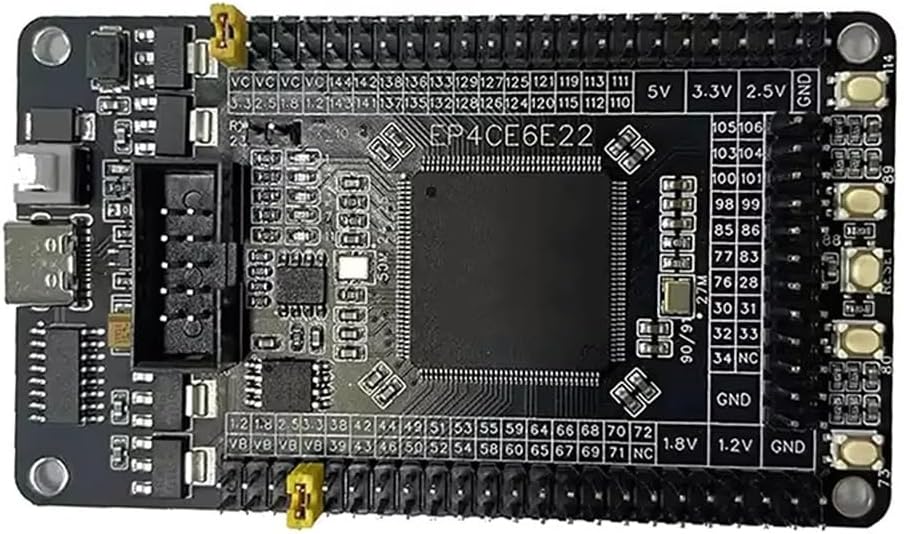
Figure 2.2.3: Top-down view of the Cwmiibili EP4CE6E22 FPGA Development Board, providing a clear perspective of all components and pin headers.
3. Setup Instructions
3.1 Powering the Board
The development board can be powered via the Type-C USB port. This port also connects to the onboard CH340 serial port chip for communication with a host computer.
3.2 Pin Voltage Selection
The board features selectable pin voltages (VC and VB) to accommodate different voltage modules. It is crucial to set these voltages correctly before downloading a program or operating the board.
- Upper Group C Pins (VC): These pins allow voltage selection using a jumper cap.
- Lower Group B Pins (VB): These pins also allow voltage selection using a jumper cap.
- Fixed 3.3V Pin: A dedicated pin provides a fixed 3.3V output.
Refer to the diagram below for the location of these voltage selection points.

Figure 3.2.1: Detailed diagram of the EP4CE6E22 Development Board, highlighting the JTAG port, Type-C port, and voltage selection jumpers for VC and VB pins.
3.3 JTAG Connection
Connect your JTAG programmer to the JTAG port on the development board. This port facilitates the connection to a Blaster downloader for programming the FPGA.
4. Operating Instructions
4.1 Programming the FPGA
The FPGA on this board is an Altera Cyclone IV EP4CE6E22. To program the FPGA:
- Ensure the board is powered and the VC and VB pin voltages are correctly set using jumper caps.
- Connect a JTAG programmer to the JTAG port on the board.
- Use appropriate FPGA development software (e.g., Intel Quartus Prime) to compile your design and generate the programming file.
- Download the program to the FPGA via the JTAG interface.
4.2 Storing Programs in EPCS Memory
The FPGA will lose its program data upon power loss. To retain your program, you must flash it to the onboard EPCS memory chip (W25Q). After flashing the program to the EPCS memory, you will need to power cycle the board for the program to load from the EPCS memory into the FPGA.
5. Maintenance
To ensure the longevity and reliable operation of your development board, observe the following maintenance guidelines:
- Keep the board clean and free from dust and debris. Use a soft, dry brush or compressed air for cleaning.
- Store the board in an anti-static bag when not in use to prevent electrostatic discharge (ESD) damage.
- Avoid exposing the board to extreme temperatures or humidity.
- Handle the board by its edges to minimize contact with components and solder joints.
6. Troubleshooting
If you encounter issues with your development board, consider the following troubleshooting steps:
- Power Issues: Ensure the Type-C cable is securely connected and providing adequate power. Check for any visible damage to the power input or cable.
- Programming Errors: Verify that your JTAG programmer is correctly connected and recognized by your development software. Confirm that the VC and VB pin voltages are set appropriately for your design.
- Program Not Retained: If your program disappears after a power cycle, ensure you have successfully flashed it to the onboard EPCS memory chip. Remember to power cycle the board after flashing to EPCS.
- Component Malfunction: Inspect the board for any visible signs of damage, such as bent pins, burnt components, or loose connections.
For persistent issues, consult online forums or the manufacturer's support resources.
7. Specifications
| Feature | Specification |
|---|---|
| Model Name | FPGA Core Board |
| Manufacturer Model Number | I500894113 |
| FPGA Chip | Altera Cyclone IV EP4CE6E22 |
| Crystal Oscillators | 1x 50MHz, 1x 27MHz |
| Communication Interface | JTAG, USB (via CH340 serial chip) |
| Onboard Memory | W25Q (EPCS) |
| User I/O | 5 LEDs, 5 Pull-up Buttons |
| Dimensions (Approx.) | 10 cm x 5 cm (3.94 in x 1.97 in) |
| Item Weight | 31 Grams |

Figure 7.1: Dimensions of the Cwmiibili EP4CE6E22 FPGA Development Board.
8. Warranty and Support
This product is covered by a standard manufacturer's warranty against defects in materials and workmanship. For specific warranty terms and conditions, please refer to the documentation provided at the time of purchase or contact your retailer.
For technical support, troubleshooting assistance, or inquiries regarding product functionality, please contact Cwmiibili customer service or your product vendor. Please have your model number (I500894113) and purchase information ready when seeking support.