1. Introduction
This instruction manual provides detailed guidance for the assembly and operation of the Reland Sun ICL8038 Monolithic Function Signal Generator Module DIY Kit. This kit allows users to construct a signal generator capable of producing sine, triangle, and square waveforms with adjustable frequency, duty cycle, and sine wave distortion.
Note: Assembly of this kit requires basic soldering skills and familiarity with electronic components.
2. Safety Information
- Always disconnect power before making any connections or adjustments.
- Ensure proper ventilation when soldering.
- Wear appropriate eye protection during assembly.
- Handle electronic components with care to avoid damage from static electricity.
- Verify all connections before applying power to prevent short circuits or component damage.
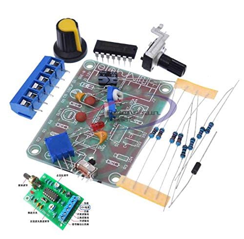
3. Kit Contents
The DIY kit includes the following components:
- ICL8038 ASIC chip
- Printed Circuit Board (PCB)
- Resistors (various values)
- Capacitors (various values)
- Potentiometers (RP1, RP2, RP3 for frequency, duty cycle, and distortion adjustment)
- Toggle Switch (S for frequency band selection)
- Terminal Blocks (for power input X1 and waveform outputs X2, X3)
- Knob for potentiometer
- Other small electronic components as required for the circuit.
4. Assembly Instructions (Setup)
Follow these steps carefully to assemble your ICL8038 Function Signal Generator:
- Prepare the PCB: Inspect the Printed Circuit Board (PCB) for any defects.
- Solder Resistors: Identify and solder all resistors to their designated positions on the PCB. Resistors are typically marked with color bands indicating their value.
- Solder Capacitors: Solder the capacitors. Pay attention to polarity for electrolytic capacitors (if present).
- Install ICL8038 Chip: Carefully insert the ICL8038 integrated circuit into its socket or solder it directly to the PCB, ensuring correct orientation (pin 1 usually marked with a dot or notch).
ICL8038 Pin Functions:
- Pin 1, 12: Sine waveform adjusting terminal.
- Pin 2: Sine wave output.
- Pin 3: Triangle wave output.
- Pin 4, 5: Frequency and duty cycle (or waveform asymmetry) adjustment.
- Pin 6: V+, positive power supply.
- Pin 7: Offset.
- Pin 8: Frequency adjustment input terminal.
- Pin 9: Square wave output (open collector). Requires a load resistor to the corresponding positive power supply terminal for operation. For TTL-compatible output, connect the load resistance to a +5V power supply.
- Pin 10: Timing capacitor terminal.
- Pin 11: V-, negative power supply terminal or ground. When using a positive and negative power supply, connect to the negative supply for symmetrical output around 0V. When using a single positive power supply, connect to ground for unipolar output (uniform voltage +VCC/2).
- Pin 13, 14: Empty.
- Solder Potentiometers: Solder RP1 (frequency adjustment), RP2 (duty cycle adjustment), and RP3 (sine wave distortion adjustment) to their respective locations. Attach the knob to the main frequency adjustment potentiometer (RP1).
- Install Switch S: Solder the frequency band selection switch (S) to its designated spot.
- Connect Terminal Blocks: Solder the terminal blocks for power input (X1) and waveform outputs (X2, X3).
- Final Inspection: Double-check all solder joints for cold joints or bridges. Ensure all components are correctly oriented and placed.
5. Operating Instructions
- Power Connection: Connect a 12V DC power supply to the X1 input terminal. Ensure correct polarity.
- Waveform Output: Connect an oscilloscope to the X2 or X3 output terminals to observe the generated waveforms (sine, triangle, square).
- Frequency Adjustment: Use potentiometer RP1 to adjust the output frequency. The kit is designed for a frequency range of 50Hz to 5KHz.
- Frequency Band Selection: Use switch S to select between the two frequency bands.
- Duty Cycle Adjustment: Use potentiometer RP2 to adjust the duty cycle of the output waveform.
- Sine Wave Distortion Adjustment: Use potentiometer RP3 to fine-tune and minimize distortion in the sine wave output.
6. Maintenance
- Keep the module clean and free from dust.
- Store in a dry environment, away from extreme temperatures and humidity.
- Avoid dropping or subjecting the module to physical shock.
- Periodically check solder joints for integrity, especially if the module is frequently handled.
7. Troubleshooting
| Problem | Possible Cause | Solution |
|---|---|---|
| No output waveform | Incorrect power connection; faulty component; poor solder joint. | Verify 12V DC power supply and polarity. Check all solder joints and component orientations. Test individual components if possible. |
| Distorted sine wave | RP3 not adjusted correctly. | Adjust potentiometer RP3 to minimize distortion. |
| Frequency not changing | RP1 or switch S not functioning; timing capacitor issue. | Check RP1 and switch S connections. Ensure timing capacitors are correctly installed. |
8. Specifications
- Model: ICL8038
- Input Power: 12V DC
- Frequency Range: 50Hz - 5KHz (two bands selectable via switch S)
- Output Waveforms: Sine, Triangle, Square
- Adjustments: Frequency (RP1), Duty Cycle (RP2), Sine Wave Distortion (RP3)
- Dimensions: 6cm x 4.5cm x 0.2cm (approximate PCB size)
- Weight: 26g (approximate kit weight)
9. Warranty and Support
For warranty information, technical support, or inquiries regarding replacement parts, please contact the seller or manufacturer directly. Details may be available on the product packaging or purchase documentation.


