1. Introduction
The DollaTek PCF8591 AD/DA Converter Sensor Module is a versatile 8-bit data acquisition device designed for use with microcontrollers like Arduino and Raspberry Pi. It features four analog inputs, one analog output, and communicates via an I2C-bus serial interface. This module is ideal for projects requiring analog-to-digital (AD) conversion for sensor readings and digital-to-analog (DA) conversion for controlling analog devices.
The PCF8591 chip operates on a single supply and offers low standby current. Its hardware address can be programmed using three address pins (A0, A1, A2), allowing up to eight devices to be connected to the same I2C bus without additional hardware. Data transfer is handled serially over the two-line bidirectional I2C bus.
2. Key Features
- Supports 4-line external voltage input acquisition (0 to 5V) with a single power supply.
- Standard double-sided PCB, 1.16mm thickness, with elegant layout and 3mm holes at each corner for easy fixing.
- Utilizes an 8-bit successive approximation A/D converter.
- Input/output via an I2C bus.
- Operating Voltage: 2.5-6V DC.
- PCB Size: 3.5 x 2.2 cm.
- Low standby current.
- Addressable via 3 hardware pins (A0, A1, A2).
- Sampling rate determined by I2C-bus speed.
- 4 analog inputs programmable as single-ended or differential inputs.
- Automatic channel selection increment.
- Analog voltage range from VSS to VDD.
- On-chip track and hold circuit.
- Multiplying DAC with one analog output.
3. Package Contents
The package includes:
- 1x DollaTek PCF8591 AD/DA Converter Sensor Module
- Connecting cable (typically 20 cm)

Figure 1: DollaTek PCF8591 module showing its dimensions (3.5cm x 2.2cm) and an included 20cm connecting cable. This image provides a clear view of the module's physical size and the type of cable supplied.
4. Setup Guide
This section outlines the steps to connect and prepare your DollaTek PCF8591 module for use with a microcontroller like Arduino or Raspberry Pi.
4.1 Module Overview
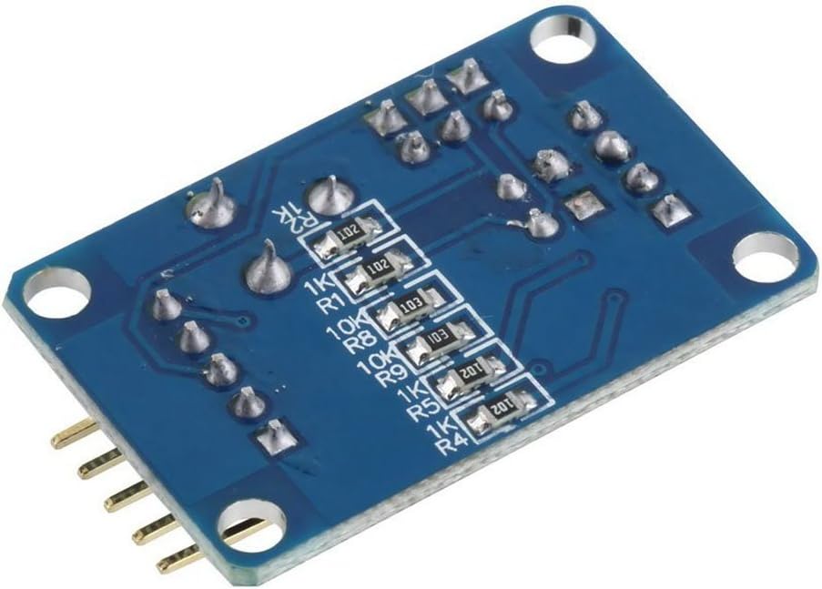
Figure 2: Top view of the DollaTek PCF8591 module, highlighting the various pins and integrated components. On the left, you can see the analog input/output pins (AOUT, AIN0-AIN3). On the right, the I2C communication pins (SCL, SDA), power (VCC), and ground (GND) are visible. A potentiometer, a photoresistor, and a thermistor are also integrated on the board for easy testing.

Figure 3: Bottom view of the DollaTek PCF8591 module, showing the arrangement of surface-mount resistors and other components on the underside of the PCB. This view illustrates the compact design and double-sided nature of the circuit board.
4.2 Pinout Description
| Pin | Description |
|---|---|
| VCC | Power supply (2.5V - 6V DC) |
| GND | Ground |
| SDA | I2C Serial Data Line |
| SCL | I2C Serial Clock Line |
| AIN0 | Analog Input Channel 0 (often connected to potentiometer) |
| AIN1 | Analog Input Channel 1 (often connected to photoresistor) |
| AIN2 | Analog Input Channel 2 (often connected to thermistor) |
| AIN3 | Analog Input Channel 3 (available for external input) |
| AOUT | Analog Output |
4.3 Connecting to Arduino/Raspberry Pi
Follow these steps to connect the PCF8591 module to your microcontroller:
- Power Connection: Connect the VCC pin of the PCF8591 module to the 5V (or 3.3V, depending on your microcontroller and desired voltage range) pin on your Arduino/Raspberry Pi. Connect the GND pin of the module to the GND pin on your microcontroller.
- I2C Communication:
- Connect the SDA pin of the PCF8591 to the SDA (Data Line) pin on your microcontroller. For Arduino Uno, this is A4. For Raspberry Pi, this is GPIO2.
- Connect the SCL pin of the PCF8591 to the SCL (Clock Line) pin on your microcontroller. For Arduino Uno, this is A5. For Raspberry Pi, this is GPIO3.
- Analog Inputs: Connect your external analog sensors or voltage sources to the AIN0, AIN1, AIN2, or AIN3 pins. The module has onboard components (potentiometer, photoresistor, thermistor) connected to some of these inputs for testing.
- Analog Output: If you need to output an analog voltage, connect your receiving device to the AOUT pin.

Figure 4: Schematic diagram of the PCF8591 module. This diagram illustrates the internal connections of the PCF8591 chip, including its power supply, I2C interface, analog inputs (AIN0-AIN3), and analog output (AOUT). It also shows the integrated potentiometer (R4), photoresistor (P3), and thermistor (P2) connected to the analog inputs.
5. Operating Instructions
The PCF8591 module communicates via the I2C protocol. To operate it, you will need to write code on your microcontroller to send and receive data over the I2C bus.
5.1 I2C Address
The default I2C address for the PCF8591 chip is 0x48 (7-bit address). This address can be modified by connecting the A0, A1, A2 pins to VCC or GND. The module typically has these pins hardwired or exposed for configuration.
5.2 Analog-to-Digital Conversion (ADC)
To read an analog value from one of the input channels (AIN0-AIN3):
- Send Control Byte: Write a control byte to the PCF8591 via I2C. This byte configures the ADC for single-ended or differential input, and selects the active analog input channel. For example, to read AIN0 in single-ended mode, the control byte might be
0x40(binary 01000000). - Read Data: After sending the control byte, read one byte of data from the PCF8591. This byte will contain the 8-bit digital value corresponding to the analog voltage on the selected input channel.
- Voltage Calculation: The 8-bit value ranges from 0 to 255. To convert this to a voltage, use the formula: Voltage = (ADC_Value / 255.0) * VREF, where VREF is the reference voltage (typically VCC, e.g., 5V).
The module often includes a potentiometer connected to AIN0, a photoresistor to AIN1, and a thermistor to AIN2 for easy testing of ADC functionality.
5.3 Digital-to-Analog Conversion (DAC)
To output an analog voltage via the AOUT pin:
- Send Control Byte: Write a control byte to the PCF8591, ensuring the DAC enable bit is set. For example, to enable DAC and write a value, the control byte might be
0x40(binary 01000000) followed by the data byte. - Send Data Byte: Send a second byte representing the 8-bit digital value (0-255) you want to convert to an analog voltage.
- Output Voltage: The AOUT pin will then output an analog voltage proportional to the digital value. Output Voltage = (Digital_Value / 255.0) * VREF.
Refer to the PCF8591 datasheet for detailed information on the control byte register and its various configurations. Many libraries are available for Arduino and Raspberry Pi to simplify I2C communication with the PCF8591.
6. Maintenance
The DollaTek PCF8591 module is a robust electronic component designed for long-term use. Minimal maintenance is required to ensure its optimal performance.
- Handling: Always handle the module by its edges to avoid touching the electronic components, which can be sensitive to static electricity.
- Storage: Store the module in a dry, cool environment, away from direct sunlight and extreme temperatures. If not in use for extended periods, store it in an anti-static bag.
- Cleaning: If necessary, gently clean the module with a soft, dry brush or a lint-free cloth. Avoid using liquids or abrasive cleaners.
- Power Supply: Ensure the power supply voltage remains within the specified range (2.5V - 6V DC) to prevent damage to the module.
7. Troubleshooting
If you encounter issues with your PCF8591 module, consider the following troubleshooting steps:
- Module Not Detected (I2C):
- Verify all power (VCC, GND) and I2C (SDA, SCL) connections are secure and correct.
- Check the I2C address. The default is 0x48. Use an I2C scanner sketch/program to confirm the module's address.
- Ensure your microcontroller's I2C pins are correctly configured and enabled.
- Check for proper pull-up resistors on SDA and SCL lines. Most microcontrollers have internal pull-ups, but external 4.7kΩ resistors might be needed for longer wires or multiple devices.
- Incorrect ADC Readings:
- Confirm the input voltage to the AIN pins is within the 0-5V range (or VCC if VCC is less than 5V).
- Verify the correct analog input channel is selected in your code's control byte.
- Ensure the reference voltage (VREF) used in your calculation matches the actual VCC supplied to the module.
- Check for noise on the analog input lines. Use shielded cables or add small capacitors if necessary.
- No DAC Output:
- Ensure the DAC enable bit is set in the control byte sent to the PCF8591.
- Verify the digital value being sent for conversion is within the 0-255 range.
- Check the connection to the AOUT pin.
- Module Not Powering On:
- Double-check VCC and GND connections.
- Ensure your power supply is providing the correct voltage (2.5V-6V) and sufficient current.
8. Specifications
| Specification | Value |
|---|---|
| Brand | DollaTek |
| Model Name | PCF8591 |
| Operating System Compatibility | Linux (for Raspberry Pi), Arduino IDE compatible |
| Connectivity Technology | I2C |
| Compatible Devices | Raspberry Pi, Arduino |
| Operating Voltage | 2.5V - 6V DC |
| ADC Resolution | 8-bit |
| DAC Resolution | 8-bit |
| Analog Inputs | 4 (single-ended or differential) |
| Analog Output | 1 |
| PCB Dimensions | 3.5 cm x 2.2 cm |
9. Warranty Information
The manufacturer's warranty for this product is typically 1 year. Please refer to your purchase documentation or contact your retailer for specific warranty terms and conditions. Keep your proof of purchase for any warranty claims.
10. Support
For technical assistance, additional documentation, or inquiries regarding the DollaTek PCF8591 AD/DA Converter Sensor Module, please refer to the following resources:
- Online Resources: Search for "PCF8591 Arduino tutorial" or "PCF8591 Raspberry Pi tutorial" on popular electronics forums and project websites for example code and community support.
- Manufacturer Website: Visit the official DollaTek website for product updates or further information (if available).
- Retailer Support: Contact the seller or retailer from whom you purchased the module for direct support.


